EP0942472A2 - Distributed photodiode and integrated circuit comprising said photodiode and an infrared receiver - Google Patents
Distributed photodiode and integrated circuit comprising said photodiode and an infrared receiver Download PDFInfo
- Publication number
- EP0942472A2 EP0942472A2 EP99200543A EP99200543A EP0942472A2 EP 0942472 A2 EP0942472 A2 EP 0942472A2 EP 99200543 A EP99200543 A EP 99200543A EP 99200543 A EP99200543 A EP 99200543A EP 0942472 A2 EP0942472 A2 EP 0942472A2
- Authority
- EP
- European Patent Office
- Prior art keywords
- input
- receiver
- signal
- terminal
- output
- Prior art date
- Legal status (The legal status is an assumption and is not a legal conclusion. Google has not performed a legal analysis and makes no representation as to the accuracy of the status listed.)
- Granted
Links
- 239000000758 substrate Substances 0.000 claims abstract description 65
- 238000009792 diffusion process Methods 0.000 claims abstract description 58
- 238000000034 method Methods 0.000 claims abstract description 45
- 230000008569 process Effects 0.000 claims abstract description 29
- 239000004065 semiconductor Substances 0.000 claims abstract description 16
- 239000000969 carrier Substances 0.000 claims abstract description 15
- 238000004519 manufacturing process Methods 0.000 claims abstract description 14
- 230000006798 recombination Effects 0.000 claims abstract description 4
- 238000005215 recombination Methods 0.000 claims abstract description 4
- 230000003111 delayed effect Effects 0.000 claims description 18
- 239000002019 doping agent Substances 0.000 claims description 15
- 230000001960 triggered effect Effects 0.000 claims description 12
- 239000003990 capacitor Substances 0.000 claims description 10
- 239000002184 metal Substances 0.000 claims description 10
- 229910052751 metal Inorganic materials 0.000 claims description 10
- 238000001514 detection method Methods 0.000 claims description 9
- 238000002955 isolation Methods 0.000 claims 47
- 230000007704 transition Effects 0.000 description 15
- 230000006854 communication Effects 0.000 description 14
- 238000004891 communication Methods 0.000 description 14
- 230000001052 transient effect Effects 0.000 description 13
- 230000008878 coupling Effects 0.000 description 12
- 238000010168 coupling process Methods 0.000 description 12
- 238000005859 coupling reaction Methods 0.000 description 12
- 238000013461 design Methods 0.000 description 12
- 238000010586 diagram Methods 0.000 description 12
- 230000000694 effects Effects 0.000 description 11
- 230000004044 response Effects 0.000 description 10
- 230000006870 function Effects 0.000 description 9
- 230000008901 benefit Effects 0.000 description 8
- 239000002800 charge carrier Substances 0.000 description 8
- 230000002829 reductive effect Effects 0.000 description 8
- 230000002441 reversible effect Effects 0.000 description 8
- XUIMIQQOPSSXEZ-UHFFFAOYSA-N Silicon Chemical compound [Si] XUIMIQQOPSSXEZ-UHFFFAOYSA-N 0.000 description 5
- 230000035945 sensitivity Effects 0.000 description 5
- 229910052710 silicon Inorganic materials 0.000 description 5
- 239000010703 silicon Substances 0.000 description 5
- 230000005684 electric field Effects 0.000 description 4
- 238000005516 engineering process Methods 0.000 description 4
- 230000036039 immunity Effects 0.000 description 4
- 238000012545 processing Methods 0.000 description 4
- 230000000630 rising effect Effects 0.000 description 4
- 238000010521 absorption reaction Methods 0.000 description 3
- 230000005540 biological transmission Effects 0.000 description 3
- 238000006243 chemical reaction Methods 0.000 description 3
- 230000007423 decrease Effects 0.000 description 3
- 230000009467 reduction Effects 0.000 description 3
- 238000012546 transfer Methods 0.000 description 3
- 230000001419 dependent effect Effects 0.000 description 2
- PCHJSUWPFVWCPO-UHFFFAOYSA-N gold Chemical compound [Au] PCHJSUWPFVWCPO-UHFFFAOYSA-N 0.000 description 2
- 239000010931 gold Substances 0.000 description 2
- 229910052737 gold Inorganic materials 0.000 description 2
- 230000031700 light absorption Effects 0.000 description 2
- 230000007246 mechanism Effects 0.000 description 2
- 230000003287 optical effect Effects 0.000 description 2
- 238000013386 optimize process Methods 0.000 description 2
- 230000010363 phase shift Effects 0.000 description 2
- 230000001360 synchronised effect Effects 0.000 description 2
- 230000005653 Brownian motion process Effects 0.000 description 1
- 230000002411 adverse Effects 0.000 description 1
- 238000013459 approach Methods 0.000 description 1
- 230000009286 beneficial effect Effects 0.000 description 1
- 230000007175 bidirectional communication Effects 0.000 description 1
- 230000000903 blocking effect Effects 0.000 description 1
- 238000005537 brownian motion Methods 0.000 description 1
- 230000001413 cellular effect Effects 0.000 description 1
- 239000004020 conductor Substances 0.000 description 1
- 230000010485 coping Effects 0.000 description 1
- 238000012937 correction Methods 0.000 description 1
- 230000001808 coupling effect Effects 0.000 description 1
- 238000000586 desensitisation Methods 0.000 description 1
- 230000008713 feedback mechanism Effects 0.000 description 1
- 238000001914 filtration Methods 0.000 description 1
- 238000005286 illumination Methods 0.000 description 1
- 230000006872 improvement Effects 0.000 description 1
- 230000010354 integration Effects 0.000 description 1
- 230000000670 limiting effect Effects 0.000 description 1
- 239000000463 material Substances 0.000 description 1
- 230000005012 migration Effects 0.000 description 1
- 238000013508 migration Methods 0.000 description 1
- 230000000116 mitigating effect Effects 0.000 description 1
- 230000003071 parasitic effect Effects 0.000 description 1
- 230000036961 partial effect Effects 0.000 description 1
- 230000002093 peripheral effect Effects 0.000 description 1
- 230000002035 prolonged effect Effects 0.000 description 1
- 230000001105 regulatory effect Effects 0.000 description 1
- 230000002123 temporal effect Effects 0.000 description 1
- 238000012360 testing method Methods 0.000 description 1
Images





Classifications
-
- H—ELECTRICITY
- H10—SEMICONDUCTOR DEVICES; ELECTRIC SOLID-STATE DEVICES NOT OTHERWISE PROVIDED FOR
- H10F—INORGANIC SEMICONDUCTOR DEVICES SENSITIVE TO INFRARED RADIATION, LIGHT, ELECTROMAGNETIC RADIATION OF SHORTER WAVELENGTH OR CORPUSCULAR RADIATION
- H10F77/00—Constructional details of devices covered by this subclass
- H10F77/93—Interconnections
- H10F77/933—Interconnections for devices having potential barriers
-
- H—ELECTRICITY
- H04—ELECTRIC COMMUNICATION TECHNIQUE
- H04B—TRANSMISSION
- H04B10/00—Transmission systems employing electromagnetic waves other than radio-waves, e.g. infrared, visible or ultraviolet light, or employing corpuscular radiation, e.g. quantum communication
- H04B10/11—Arrangements specific to free-space transmission, i.e. transmission through air or vacuum
- H04B10/114—Indoor or close-range type systems
-
- H—ELECTRICITY
- H04—ELECTRIC COMMUNICATION TECHNIQUE
- H04B—TRANSMISSION
- H04B10/00—Transmission systems employing electromagnetic waves other than radio-waves, e.g. infrared, visible or ultraviolet light, or employing corpuscular radiation, e.g. quantum communication
- H04B10/40—Transceivers
-
- H—ELECTRICITY
- H10—SEMICONDUCTOR DEVICES; ELECTRIC SOLID-STATE DEVICES NOT OTHERWISE PROVIDED FOR
- H10F—INORGANIC SEMICONDUCTOR DEVICES SENSITIVE TO INFRARED RADIATION, LIGHT, ELECTROMAGNETIC RADIATION OF SHORTER WAVELENGTH OR CORPUSCULAR RADIATION
- H10F30/00—Individual radiation-sensitive semiconductor devices in which radiation controls the flow of current through the devices, e.g. photodetectors
- H10F30/20—Individual radiation-sensitive semiconductor devices in which radiation controls the flow of current through the devices, e.g. photodetectors the devices having potential barriers, e.g. phototransistors
- H10F30/21—Individual radiation-sensitive semiconductor devices in which radiation controls the flow of current through the devices, e.g. photodetectors the devices having potential barriers, e.g. phototransistors the devices being sensitive to infrared, visible or ultraviolet radiation
- H10F30/22—Individual radiation-sensitive semiconductor devices in which radiation controls the flow of current through the devices, e.g. photodetectors the devices having potential barriers, e.g. phototransistors the devices being sensitive to infrared, visible or ultraviolet radiation the devices having only one potential barrier, e.g. photodiodes
- H10F30/221—Individual radiation-sensitive semiconductor devices in which radiation controls the flow of current through the devices, e.g. photodetectors the devices having potential barriers, e.g. phototransistors the devices being sensitive to infrared, visible or ultraviolet radiation the devices having only one potential barrier, e.g. photodiodes the potential barrier being a PN homojunction
-
- H—ELECTRICITY
- H10—SEMICONDUCTOR DEVICES; ELECTRIC SOLID-STATE DEVICES NOT OTHERWISE PROVIDED FOR
- H10F—INORGANIC SEMICONDUCTOR DEVICES SENSITIVE TO INFRARED RADIATION, LIGHT, ELECTROMAGNETIC RADIATION OF SHORTER WAVELENGTH OR CORPUSCULAR RADIATION
- H10F77/00—Constructional details of devices covered by this subclass
- H10F77/10—Semiconductor bodies
- H10F77/14—Shape of semiconductor bodies; Shapes, relative sizes or dispositions of semiconductor regions within semiconductor bodies
Definitions
- the present invention relates to a photodiode which can be fabricated using standard semiconductor fabrication techniques.
- Infrared wireless data communication is a useful method for short range (in the approximate range of 0-10 meters) wireless transfer of data between electronic equipment; such as, cellular phones, computers, computer peripherals (printers, modems, keyboards, cursor control devices, etc.), electronic keys, electronic ID devices, and network equipment.
- Infrared wireless communication devices typically have the advantages of smaller size, lower cost, fewer regulatory requirements, and a well defined transmission coverage area as compared to radio frequency wireless technology (i.e. the zone of transmission is bounded by physical walls and therefore more useful in an office environment).
- infrared wireless communication has further advantages with regard to reliability, electro-magnetic compatibility, multiplexing capability, easier mechanical design, and convenience to the user as compared to cable based communication technology.
- infrared data communication devices are useful for replacing 0-10 meter long data transfer cables between electronic devices, provided that their size and costs can be reduced to that of comparable cable technology.
- IrDA Infrared Data Association
- Physical Layer Link Specification 1.1e specifies two main physical layer infrared modulation protocols.
- the IrDA Physical Layer Link Specification 1. le also specifies two modes for modulation of data on the infrared transmitted signal.
- One mode is a low-speed (2 Kbp/s to 1.15 Mbp/s) on-off infrared carrier using synchronous modulation where the presence of a pulse indicates a 0 bit and the absence of a pulse indicates a 1 bit.
- the second mode is a high speed (4Mb/s) synchronous Four Pulse Position Modulation (4PPM) method in which the time position of a 125 nS infrared pulse in a 500 nS frame encodes two bits of information.
- the 1.1e specification also specifies a preamble pattern which is sixteen repeated transmissions of a predetermined set of symbols.
- Infrared data communications devices typically consist of transmitter and receiver components.
- the infrared data transmitter section consists of one or more infrared light emitting diodes (LEDs), an infrared lens, and an LED current driver.
- a conventional infrared data receiver typically consists of an infrared photodiode and a high gain receiver amplifier with various signal processing functions, such as automatic gain control (AGC), background current cancelling, filtering, and demodulation.
- AGC automatic gain control
- background current cancelling filtering
- demodulation demodulation
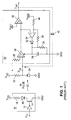
- FIG. 1A A representative example of a conventional infrared data transmitter and receiver pair is shown in FIG. 1A.
- Infrared transmitter 10 includes LED 16 which generates a modulated infrared pulse in response to transistor 14 being driven by the data signal input at D IR .
- the modulated infrared signal is optically coupled to an infrared detector, such as photodiode 24 normally operated in current mode (versus voltage mode) producing an output current which is a linear analog of the optical infrared signal falling on it.
- the infrared pulses generated by LED 16 strike photodiode 24 causing it to conduct current responsive to the data signal input at D IR thereby generating a data signal received at D IR .
- the signal received at D IR is transformed into a voltage signal V IR and amplified by amplifier 26.
- the signal output from amplifier 26 then feeds into comparator 42 which demodulates the received signal by comparing it to a detection threshold voltage V DET in order to produce a digital output data signal at D OUT .
- the received signal waveform will have edges with slope and will often include a superimposed noise signal.
- V DET is ideally placed at the center of the received signal waveform so that the output data signal has a consistent waveform width despite the slope of the received signal edges.
- placing V DET at the center of the received signal improves the noise immunity of receiver 20 because the voltage difference between V DET and both the high and low levels of the received signal is maximized such that noise peaks are less likely to result in spurious transitions in D OUT .
- the received signal can vary in amplitude by several orders of magnitude due primarily to variations in the distance between transmitter 10 and receiver 20.
- the strength of the received signal decreases proportional to the square of the distance.
- the photodiode outputs signal current in the range of 5 nA to 5 mA plus DC and AC currents arising from ambient infrared sources of sunlight, incandescent and fluorescent lighting.
- AGC automatic gain control
- the received signal is fed to AGC peak detector 36 which amplifies the signal and drives current through diode 32 into capacitor 28 when the signal exceeds the AGC threshold voltage V AGC in order to generate a gain control signal.
- the gain control signal increases in response to increasing signal strength and correspondingly reduces the gain of amplifier 26 so that the amplitude of the received signal at the output of amplifier 26 remains relatively constant despite variations in received signal strength.
- infrared receiver 20 amplifies the photodetector signal current and then level detects or demodulates the signal when it rises above the detect threshold V DET thereby producing a digital output pulse at D OUT .
- the receiver may also perform the added functions of blocking or correcting DC and low frequency AC ambient (1-300uA) signals and Automatic Gain Control (AGC) which improves both noise immunity and minimizes output pulse width variation with signal strength.
- AGC Automatic Gain Control
- FIG. 1B The structure of the conventional discrete PIN photodiode 24 is illustrated in FIG. 1B.
- a wafer 50 is lightly doped with N dopant in order to produce an intrinsic region 56.
- a P+ region 52 is formed on one surface of the wafer and an N+ region 58 is formed on the opposing surface of wafer 50 with intrinsic region 56 interposed P+ region 52 and N+ region 58.
- a reflective layer 60 typically gold, is disposed on the surface containing P+ region 58 with reflective layer 60 also serving as the electrical contact to N+ region 58.
- a metal contact 54 is disposed on the surface containing P+ region 52 to provide the electrical connection to the P+ region.
- one power supply potential is applied to the reflective layer 60 and another power supply voltage is applied to contact 54 to reverse bias the PN junction formed by P+ region 52 and N+ region 18.
- This forms a large depletion region within the intrinsic region 56 wherein electron and hole charge carrier pairs generated by light photons incident upon the intrinsic region 56 are rapidly accelerated toward the P+ and N+ regions respectively by the electric field of the reverse bias voltage.
- Charge carrier pairs are also typically generated outside the depletion region within intrinsic region 56 which diffuse, due to random thermal motion of the carriers, at a much slower velocity until they reach either the depletion region or the junction formed by P+ region 52 and intrinsic region 56 of photodiode 24.
- a conventional photodiode that is designed for high quantum, i.e. light conversion, efficiency requires that the light path within the photo current collection zone, i.e. the depletion and non-depletion zones within intrinsic region 56, be sufficient in length so that most of the light photons of the incident light signal area are absorbed and converted into electron-hole pairs that are collectable at the P+ and N+ regions. Usually, this requires that the width of the intrinsic region 56, which is the primary light collection region, be several times the length required for light absorption. If diode 10 has an efficient back-side reflector, such as reflective layer 60, which effectively doubles the light path within diode 24, then the intrinsic region 56 of the photodiode can be made narrower. For a typical near infrared silicon photodiode, the nominal absorption path length is about 15-25 microns. The path length should be at least two to three times the nominal absorption path length to obtain good light conversion efficiency.
- a photodiode designed for high frequency response requires that the photo current pairs generated by the light signal be collected rapidly and that the diode RC time constant is fast. Rapid photo current pair collection usually requires that most of the photo current pairs generated by the light signal be generated with the depletion region formed by the reverse bias voltage because the pairs will have a high drift velocity. Otherwise, the photo generated charge carrier pairs produced in the non-depletion regions within intrinsic region 56 and within diffusion distance of the collection electrodes 52 and 58 will have a diffusion velocity that is several hundred times slower than the velocity of the pairs generated within the depletion zone.
- the photo generated charge carrier pairs in the non-depletion zones will slowly migrate for collection at P+ region 52 and N+ region 58 resulting in a tail on the trailing edge of the electrical signal corresponding to the light signal.
- the diffusion distance of the charge carriers is determined by the carrier mean free path before re-combination and may exceed 150 microns.
- a fast RC time constant for photodiode 24 requires minimal capacitance and low series resistance between the electrical contacts 54 and 60 and the photo current pair collection sites at the margin between P+ region 52 and the depletion zone and the margin between N+ region 58 and the depletion zone.
- lightly doped intrinsic region 56 between the P+ and N+ regions 52 and 58 results in a PIN photodiode with a wider depletion region, depending on the magnitude of the reverse bias voltage, which improves the light collection efficiency, increases speed, and reduces capacitance over that of a simple PN diode structure.
- the PIN photodiode is typically produced by diffusing the N+ region 58 on the back side of the lightly doped (N) wafer 50, diffusing the P+ region 52 on the topside of the wafer 50, and then adding metal contacts to each side of the wafer.
- the backside contact area connected to N+ region 58 is reflective layer 60 and is made of gold. The reflective layer is then typically connected to the ground voltage terminal.
- a PN diode junction can also function as a photodiode.
- the photocurrent collection region within an electric field, the drift region, in a PN photodiode is limited to the relatively thin depletion zone produced when the PN junction is reverse biased.
- This thin drift region is much less efficient in the collection of photo-generated charge carrier pairs because most of the pairs are generated outside of depletion zone.
- the charge pairs generated outside of the depletion zone thermally diffuse to collection points margins of the P and N layers and into the depletion zone at a much slower relative speed resulting in slow photodiode performance.
- the highly doped P and N regions result in high diode capacitance per unit area which further slows the performance of the photodiode.
- PIN photodiode outperforms a standard PN diode
- the PIN photodiode structure cannot be easily manufactured by standard semiconductor processes wherein fabrication is typically performed on only one side of the semiconductor wafer 50.
- transceiver IC integrated circuit
- IC integrated circuit
- a discrete infrared photodiode is typically assembled with the transceiver circuit and an LED, along with lenses for the photodiode and LED, into a plastic molded package to form a transceiver module.
- the transceiver module is designed to be small in size and allow placement in the incorporating electronic device so as to have a wide angle of view, typically through an infrared window on the transceiver casing.
- the transceiver IC is designed to digitally interface to some type of serial data communications device such as an Infrared Communication Controller (ICC), UART, USART, or a microprocessor performing the same function.
- ICC Infrared Communication Controller
- the present invention relates to a photodiode which can be fabricated using standard semiconductor fabrication processes making it suitable for integration on a semiconductor substrate with a receiver circuit.
- An embodiment of a distributed photodiode is composed of a substrate that is doped with a first dopant type and has first and second planar surfaces and a plurality of diffusions, where the plurality of diffusions is doped with a second dopant type and is formed on the first planar surface of the substrate.
- a first plurality of connective traces is disposed on the first planar surface of the substrate and is coupled to each of the plurality of diffusions.
- An embodiment of a method for producing a photodiode involves providing a substrate having first and second planar surfaces, doping the substrate with a first dopant type, diffusing a second dopant type at a plurality of sites on the first planar surface of the substrate to form a plurality of diffusions, and disposing a first set of conductive traces on the first surface planar surface to interconnect each of the plurality of diffusions.
- An embodiment of an integrated photodiode and receiver circuit includes a substrate doped with a first dopant type and having first and second planar surfaces and a plurality of diffusions, the plurality of diffusions being doped with a second dopant type and formed on the first planar surface of the substrate.
- a first plurality of connective traces is disposed on the first planar surface of the substrate and is coupled to each of the plurality of diffusions.
- a receiver circuit is formed on the substrate, where a first input terminal of the receiver circuit is coupled to the first plurality of connective traces.
- FIG. 1 is a circuit diagram of a conventional infrared transmitter receiver pair.
- FIG. 2 is a cross-sectional diagram of a conventional PIN photodiode.
- FIG. 3 is a diagram of an embodiment of an integrated receiver and a photodiode according to the present invention.
- FIG. 4A is a cross-sectional diagram of a portion of the photodiode of FIG. 3.
- FIG. 4B is a top-view diagram of a portion of the photodiode of FIG. 3.
- FIG. 5 is a diagram of an embodiment of the integrated receiver and photodiode of the present invention wherein the photodiode includes a conductive shield.
- FIG. 6 is a functional block diagram of one embodiment of an infrared receiver circuit suitable for use in the integrated receiver and photodiode of the present invention.
- FIG. 7 is a functional block diagram of another embodiment of an infrared receiver circuit suitable for use in the integrated receiver and photodiode of the present invention.
- FIG. 8 is a functional block diagram of yet another embodiment of an infrared receiver circuit suitable for use in the integrated receiver and photodiode of the present invention.
- FIG. 9 is a functional block diagram of still yet another embodiment of an infrared receiver circuit suitable for use in the integrated receiver and photodiode of the present invention.
- FIG. 10 is a functional block diagram of a further embodiment of an infrared receiver circuit suitable for use in the integrated receiver and photodiode of the present invention.
- FIG. 11 is a diagram of an embodiment of the integrated receiver and photodiode of the present invention utilizing a photodiode having an additional set of insulated traces for use with a differential input receiver.
- an IrDA receiver or transceiver with an integrated photodiode has typically not been either cost effective or sufficiently optically sensitive to have the range to meet, for example, the IrDA lowspeed specification.
- IrDA receivers typically use discrete photodiodes with areas of 3.4 to 25 square millimeters in order to produce the minimum signal level, typically 30nA to 220nA, required by the minimum detect threshold of an IrDA receiver at a range of 1 meter.
- a receiver or transceiver IC typically has an area of 2 to 10 square millimeters depending upon the IC fabrication process technology employed and the complexity of the circuit design.
- PN photodiodes can be constructed using a standard IC fabrication process, the resulting photodiodes typically suffer from reduced efficiency, signal bandwidth, or very high capacitance as compared to PIN photodiodes fabricated using a process optimized for photodiodes. Because there are significantly fewer processing steps and fewer photo-lithographic masks of low optical resolution required for a photodiode optimized process, a PIN photodiode specific silicon process typically costs about one half or less per unit area than a modern silicon IC process. In addition, because process yields are higher and testing is simpler for a photodiode specific process, there is a further reduction in cost per area of perhaps another 20% to 40%.
- the processing and yield cost advantages of the photodiode specific process are partially offset by the assembly cost incurred in the handling, inventory, die attachment, and bonding of the discrete photodiode into a receiver or transceiver module.
- the photodiodes in an IrDA receiver or transceiver are significantly larger than the receiver or transceiver IC and the photodiodes can be fabricated as discrete devices at lower cost per unit area.
- it is more cost effective not to integrate the photodiodes with the receiver or transceiver, despite the savings obtained by eliminating the photodiode assembly cost.
- PIN photodiodes constructed using a standard IC process will have a light conversion efficiency per unit area which is typically 20% to 80% of the efficiency of a PN photodiode fabricated using a photodiode specific process.
- the integrated diode must be less than half the area of an external photodiode in order for an integrated photodiode and receiver or transceiver IC to be more cost effective than a discrete photodiode solution.
- the integrated photodiode will therefore have a signal output that is only 10% to 40% of the signal output of a cost-equivalent discrete PIN photodiode.
- a photodiode fabricated on a standard IC process typically has a capacitance per unit area that is over 100 times higher than the capacitance per unit area of a photodiode fabricated using a process optimized for photodiodes. This increased capacitance causes a significant reduction in the infrared receiver noise/bandwidth performance which in turn requires the use of a larger integrated photodiode than would otherwise be required.
- the smallest photodiode signal current which can be detected, given a particular receiver bandwidth, must be greater than the equivalent input noise level of the receiver. Hence, if the receiver's noise level can be reduced then a smaller received signal can be detected.
- the lower bound on an IC receiver's equivalent input noise level is limited by the input transistor noise performance and area, supply voltage, input device bias currents and the source impedance, which is determined by signal frequency and photodiode capacitance.
- the principles of low noise photodiode amplifier design, which govern the input noise parameters, are well known to those skilled in the art and will not be expanded upon here.
- a four times increase in the input capacitance of the photodiode will typically result in a two times increase in the equivalent input noise current of a receiver including the photodiode when the receiver is optimized for minimum noise within the same bandwidth.
- increasing the area of a photodiode by four times increases the output current gain by four times although it only increases the input noise by two times. Consequently, increasing a photodiode area increases its effective gain, or signal-to-noise ratio, for a given signal illumination level.
- the receiver input noise current of an optimized receiver is increased by 10 fold and therefore requires the minimum detect threshold of the receiver to be increased by 10 fold.
- a photodiode can be constructed using a standard IC process to have only a moderately degraded efficiency as compared to a photodiode constructed using a photodiode optimized process, the 100 fold larger capacitance of the standard IC process photodiode degrades the receiver noise performance so as to effectively reduce input sensitivity by 10 fold.
- an efficient photodiode typically uses the substrate as one of the diode contacts because the light absorption depth of the silicon typically exceeds by several times the shallow junctions on standard IC processes. Since the substrate contact is typically P material, this means that the substrate is an anode connection, which is the reverse of standard external photodiode structure which usually have cathode connections to the substrate. Consequently, an integrated photodiode receiver typically needs to be able to function with the anode to substrate, which is usually coupled to a ground potential supply rail.
- an IrDA receiver with sufficient sensitivity and bandwidth to operate using a small photodiode integrated on the same IC.
- a small photodiode integrated on the same IC.
- such a receiver might use a cost effective integrated photodiode of about 2 mm 2 in area.
- the integrated photodiode would output about a 18nA pulse when suitably lensed and illuminated with 4uW/cm 2 of infrared light, which is the minimum infrared irradiation level specified for IrDA slow speed operation with a 10 -8 bit error rate.
- the receiver utilizing the integrated photodiode requires an equivalent input noise level over the pulse bandwidth of about 2nA and a signal detection threshold of about 9nA.
- a major problem for the design of IrDA infrared receivers is output feedback noise.
- the integrated photodiode is vulnerable to feedback capacitance from the receiver output D OUT to the photodiode.
- an integrated photodiode of 2 mm 2 will have a feedback coupling capacitance in the range of 2 to 10 femto Farads (fF) between the upper surface of the photodiode and the surface of the receiver output bonding wire, which will typically be less than 2 mm distance away.
- fF femto Farads
- the integrated photodiode is smaller than a discrete external photodiode, the integrated photodiode is necessarily located closer to the receiver output because it is on the same IC as the receiver circuit. Consequently, the feedback coupling capacitance is of the same order of magnitude as an external photodiode.
- the receiver must be more sensitive to compensate for the smaller and less efficient integrated photodiode, the effects of feedback are proportionately larger.
- the feedback capacitance is as little as 2 femto Farad and the receiver output has a 5V swing
- 10 femto Coulombs (fC) of charge will be transferred to the receiver input terminal for each transition at the receiver output terminal.
- the receiver bandwidth is 600kHz, which is a typical value for a 115 Kbps lowspeed IrDA receiver
- the time constant of the signal transient is (1/600 kHz)/6.28 or about 265 nsec. Consequently, the 10 fC of charge will have an apparent current amplitude of (10fC/265nsec) or 376nA. Notice that this is over 40 times the minimum detect threshold of 9nA in the above example and will cause disruption of the input signal over 80% of the operating range of the receiver.
- Some of the conventional remedies for output to input feedback problems of IrDA receivers are: 1) to use a large photodiode so that the output feedback is proportionately small compared with the signal; 2) install shielding between the output and the input photodiode; and 3) balanced differential output lines and/or balanced input photodiodes. All of these solutions entail increased cost either due to increases in total photodiode area, increased package complexity, or the cost of adding a shield.
- Another receiver output to photodiode input feedback mechanism not present with an external photodiode but which may be present with an infrared receiver integrated with an on-chip photodiode is feedback coupling through the substrate. This may be due to either carriers injected by the receiver circuitry or by distributed RC coupling through the substrate.
- external shielding will not work, although some benefit can be had by placing diffused P and N collector rings connected to suitable supply voltages. These act either as limited substrate shields or as collectors for substrate carriers.
- FIG. 3 illustrates an embodiment of an integrated receiver and photodiode 300 according to the present invention.
- a photodiode 330 is constructed by forming the PN junctions of photodiode 330 from N-diffusion dots 332 spaced from one another and connected to one another using conductive traces 334.
- N-diffusion dots 332A, 332B and 332C will be discussed in detail but are illustrative of the totality of N-diffusion dots 332 which make up photodiode 330.
- the connective traces 334 are coupled to the input terminal D IR of receiver 220.
- the output terminal D OUT of receiver 220 is capacitively coupled, represented by capacitor 40, to photodiode 330 and a feedback control receiver design can be utilized to reduce the effects of feedback.
- a feedback control receiver design can be utilized to reduce the effects of feedback.
- FIG. 4A is a partial cross sectional view of an embodiment of the photodiode 330 of FIG. 3.
- Multiple N-diffusions 332A, 332B and 332C are formed in P-substrate 210 at regular intervals to form the PN junctions of photodiode 330.
- the N-diffusions are formed from minimum geometry dots of width W spaced at a uniform distance D from each other and are then connected together with minimum capacitance interconnects 334A, 334B and 334C, respectively, which can be formed using upper metal layer minimum geometry traces.
- the junction dot spacing D is determined by the mean free carrier diffusion path and the maximum pulse decay time constant for the receiver.
- the mean free carrier diffusion path length is 155 microns and the diffusion velocity of carriers is 300 m/sec and if the N-diffusion dots 332A-C are separated by 50 microns, then the maximum diffusion distance of light generated carriers to a junction dot is about 25 microns, i.e. 50 microns divided in half.
- the pulse decay time constant is approximately 1.2 usec, the time for the carriers to diffuse 25 microns.
- the minimum diffusion dot size is approximately 2 X 2 microns. If N-diffusion dots 332A-C are placed every 50 X 50 microns, then the diffusion junction of photodiode 330 occupies less than 1/500 of the area of the photodiode. The resulting capacitance from the N-diffusion dots 332 to substrate 210 of photodiode 330 is about 1/80 of a comparably sized photodiode having a continuous junction. The capacitance to substrate 210 is larger than the junction area ratio due to the added capacitance of the N-diffusion sidewalls and the capacitance of the minimum geometry metal interconnects 334A-C.
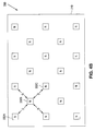
- FIG. 4B is a top view of photodiode 330 which illustrates the distribution of N-diffusion dots on a surface of P-substrate 210.
- N-diffusion dots 332A-C are spaced at uniform distance D from one another. All the N-diffusion dots are equally spaced and connected via interconnects 334A-C to form photodiode 330.
- the distributed structure of photodiode 330 tends to extend the duration of the infrared pulse by about one half the carrier decay time constant, thus it is beneficial to reduce the output pulse width by this amount to restore the output pulses to the input pulse width.
- the spacing D of the N-diffusion dots 332 can be varied in order to adjust the response speed of the photodiode 330.
- the connective traces 334 shown in FIGS. 3 and 4A are typically metal strips that are approximately 1 micron wide and spaced at 43 micron intervals.
- the metal of the connective traces 334 occupies approximately 1/40 of the amount of surface that would be covered by a conductive layer for a conventional continuous diode.
- the connective traces 334 present a smaller antenna for noise signal reception and the capacitive coupling to the feedback signal from the output terminal D OUT and external noise sources is also reduced.
- An advantage of the N-diffusion dot method illustrated in the photodiode 330 of FIGS. 4A and 4B is that its effective coupling capacitance to external noise sources and internal substrate RC coupling effects is significantly reduced. (However, it does not provide immunity from substrate carrier noise injected by circuits of the receiver or transmitter also fabricated on substrate 210.)
- the coupling capacitance is on the order of 1/50 of the area of the photodiode which results in a significant improvement in the signal to noise ratio of the integrated receiver.
- the exposed portions of substrate 210 between the N-diffusion dot connections 334A-C also act as an effective shield with the addition of grounded backplane 212 to photodiode 330 shown in FIG. 4A. Without the backplane, the screen created by the metal interconnect would have similar coupling capacitance to external noise sources as a continuous conductor over the same area. However, in the present invention, the grounded backplane 212 sets up an inverted induced noise signal which neutralizes the noise signal in the field around connective traces 334. As a result, the only noise signal that remains to generate a noise difference signal in a receiver circuit is the 1/40th of the area of the backplane 212 that is shadowed by the connective traces 334.
- the efficiency of the N-diffusion dots 332 in absorbing thermally migrating photo-generated charge carrier pairs within P-substrate 210 is only about 20% less than that of a continuous N-diffusion region.
- the heavily doped PN junction formed in diodes formed using standard semiconductor processes result in a depletion layer at the PN junction of only 1 micron.
- the absorption depth of the incident light is approximately 15 microns.
- the grounded P-substrate 210 effectively shields these carriers from electrical fields and so the carriers thermally wander, i.e. the carriers are subject to Brownian motion, without the effect of electrical fields upon them.
- each of the photo-generated carriers in P-substrate 210 can be viewed as being at the center of a spherical cloud representing the probability distribution for the thermal migration of that carrier.
- This spherical cloud has a radius of approximately 150 microns, the average distance travelled by the carriers before recombination.
- the probability that each carrier will reach the PN junction of one of the N-diffusion dots 332 before recombining is only slightly reduced.
- the distributed structure of photodiode 330 is only marginally less efficient that a comparable photodiode having a continuous PN junction while the capacitance of photodiode 330 is significantly reduced.
- FIG. 5 illustrates the integrated photodiode 330 and receiver 220 shown in FIG. 3 with the addition of a conductive shield 502.
- the shielding of photodiode 330 can be improved with only a modest increase in photodiode capacitance by disposing conductive shield traces 502A-D above the N-diffusion dots 332 and interconnect traces 334.
- the conductive shield traces 502A-D are then coupled to a ground potential to thereby ground any noise signal that is incident upon the conductive shield 502.
- the conductive shield traces 502A-D are typically fabricated using a second metal layer of the semiconductor fabrication process.
- the addition of conductive shield traces 502A-D to photodiode 330 increases the photodiode capacitance by approximately 50%. However, conductive shield 502 also shields approximately 10dB of the external noise signal incident upon photodiode 330.
- photodiode 330 may be high enough to permit the use of a conventional receiver circuit such as receiver 20 of FIG. 1 as receiver 220 fabricated on the same substrate. In that case, photodiode 330 would be substituted for photodiode 24 in the circuit of FIG. 1, but both photodiode 330 and receiver circuit 20 would be fabricated on the same semiconductor substrate.
- FIG. 6 illustrates one embodiment of a receiver circuit 420 designed to mitigate the effects of feedback through control of the feedback phase with the design of the receiver bandwidth filter design such that receiver circuit 420 is suitable for use as the receiver circuit 220 of FIG. 3.
- a receiver circuit 420 designed to mitigate the effects of feedback through control of the feedback phase with the design of the receiver bandwidth filter design such that receiver circuit 420 is suitable for use as the receiver circuit 220 of FIG. 3.
- on-off modulation such as the modulation specified by IrDA
- the receiver This is accomplished by designing the receiver so that the feedback from the data output is positive such that the feedback actually reinforces the received signal because the polarity of the feedback spike corresponds to the polarity of the received signal. If the receiver transient response has little overshoot, and either no AGC or high signal threshold AGC is used, then the positive feedback acts as dynamic hysteresis, producing an output pulse without any spurious transitions.
- the infrared receiver 420 of FIG. 6 is designed so that the feedback through parasitic capacitor 440 from D OUT to the photodiode input D IR is positive. Thus, a negative transition in the received signal at D IR results in a negative transition in the data output signal at D OUT which will, in turn, generate a corresponding negative spike in the feedback signal.
- the received signal is countered by the much larger amplitude of the feedback spike which causes the signal at the input of detect comparator 442 to cross the detect threshold V DET repeatedly. This results in multiple transitions in data output signal thereby corrupting the data.
- the positive feedback reinforces the received signal.
- the positive feedback when combined with the received signal at D IR , results in a signal at the input of comparator 442 that swings farther away from V DET responsive to the edges in D IR generating a single output pulse at D OUT .
- Bandpass filter 434 must be designed for good damped transient response to suppress signal ringing and overshoot.
- An example of a suitable filter is a Gaussian bandpass filter, which has roll-off edges in the signal output from the filter that have low ringing and overshoot transient response.
- the filter will temporally spread out the energy contained in the feedback spike. For example, a 20 nsec. spike is transformed into a 300 nsec. spike, which further contributes to the dynamic hysteresis discussed above.
- the AGC threshold V AGC of receiver 420 needs to be set above the peak feedback value by a margin adequate to prevent the peak feedback value from causing the gain to be adjusted downward by the AGC.
- AGC noise quieting which reduces signal interference from noise
- the output pulse width will vary more with signal level.
- AGC reduces the front end gain of amplifier 426 responsive to an increasing input signal on D IR .
- amplifier 426 will be highly sensitive because the AGC permits the gain to be high.
- the AGC will reduce the gain in response to the input signal including the noise level. This improves the noise immunity of the receiver 420.
- the receiver will function so long as the received signal strength is greater than the amplitude of the noise. From a practical standpoint, in a noisy environment, this permits the sending and receiving devices to be moved closer together to strengthen the received signal and the communications link will be able to function.
- the noise level will prevent the receiver from capturing the transmitted signal without corruption of the output data signal even when the transmitting device and receiver are close together because the noise signal will still have high enough amplitude to cause spurious output transitions in between valid output transitions.
- AGC improves the fidelity of the pulses in the data output D OUT ⁇ Despite careful filter design, some ringing, overshoot and undershoot will still occur in the receiver. AGC reduces the effect of ringing, overshoot and undershoot when it reduces the sensitivity of amplifier 426. Further, because there is also ramping on the received waveform which can cause widening or narrowing of the signal pulse unless the detect threshold V DET is in the center of the waveform, AGC improves the fidelity of the pulse by maintaining V DET at the center of the waveform.
- the amplitude of the positive feedback also causes the AGC to adjust the receiver sensitivity downward.
- the AGC reduces the gain in response to the positive feedback, the sensitivity of the receiver to the transmitted signal is also reduced and, particularly at high signal pulse rates, can cause the receiver to lose the input signal.
- the receiver circuit of FIG. 6 is effective in reducing the effects of feedback, it still suffers from the effect of feedback transient overshoot or ringing, which, if it exceeds the detect level V DET , will cause undesirable extraneous output pulse transitions.
- V DET detect level
- filter design techniques can limit transient overshoot to a negligible level, in practice, reducing it to a value below 1/5 or 1/10 the peak level is difficult due to variable phase shift effects both within and outside the infrared receiver.
- Some of these variable phase shift effects are due to normal variances in parameters such as transmit pulse shape, photodiode time constant, photodiode capacitance, receiver output load capacitance, receiver supply voltage, and filter component values.
- Receiver 420 can beneficially decrease the disruptive effects of feedback by 10db-20db for infrared receivers used with edge triggered, serial data communication controllers which do not need an accurate data pulse width or with receiver systems which do not require the benefits of a low threshold AGC.
- Infrared receiver 620 which is suitable for the use of low threshold AGC, adds delay 650 to the output signal from comparator 642, typically delaying the output by 1 ⁇ 2 of the pulse interval of the data signal to permit decay of the feedback pulse.
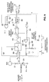
- Receiver 620 also includes a signal disable switch 648 controlled by AGC disable one-shot 652 which blocks the signal to the AGC input upon the leading edge of an output pulse transition on D OUT ⁇
- AGC disable one-shot 652 By delaying the output signal, the peaks of the feedback signal from D OUT to D IR are shifted in time so that the feedback peak occurs toward the center of the pulse in the received signal at D IR ⁇
- AGC disable one-shot 652 generates a signal disable pulse responsive to the falling edge in the output signal at D OUT which causes AGC disable switch 648 to open and isolate the input of AGC peak detector 636 from the received signal path for the duration of the signal disable pulse.
- the signal disable pulse must persist for a time interval sufficient for the feedback transient to settle below levels which would cause AGC gain reduction.
- AGC peak detector 636 is therefore isolated from the signal path at the time that the feedback pulse appears at the negative input to comparator 642. As a result, the gain control voltage stored in capacitor 628 during the disable period reflects the received signal strength and is not corrupted by the feedback signal.
- the AGC disable one-shot 652 may be replaced with an output edge triggered disable one shot which will generate a disable pulse responsive to both the falling and rising edges of the output signal at D OUT .
- An edge triggered disable will isolate the AGC peak detector 636 during feedback pulses for both the edges of the output pulse at D OUT .
- receiver 620 is substantially better than the performance of conventional receivers, it requires that receiver 620 be designed so that the feedback from D OUT to D IR is positive. Negative feedback will still cause spurious transitions in the output signal because the feedback is coupled to the input of comparator 642.
- Receiver 820 of Fig. 8 shows yet another embodiment of a single input receiver circuit suitable for use as the receiver 220 in the present invention but where the design of receiver 820 is not dependent upon positive feedback from output terminal D OUT to input terminal D IR .
- Signal disable switch 848 is positioned between the output of bandpass filter 834 and the inputs of both comparator 842 and AGC peak detector 836.
- Output edge triggered disable one-shot 852 receives the delayed output signal at D OUT and generates a disable pulse responsive to each of the falling and rising edges of the output signal. The disable signal must persist for a period long enough for the feedback transients to decay below a level that would cause spurious transitions in the output signal from comparator 842.
- the disable pulses cause signal disable switch 848 to isolate comparator 842 and AGC peak detector 836 from the received signal path during the times when the falling and rising feedback peaks are present at the output of bandpass filter 834.
- This configuration permits receiver 820 to obtain the improved AGC performance of receiver 620.
- receiver 820 is not dependent upon positive feedback because the input of comparator 842 is isolated from the feedback peaks, thereby preventing the negative feedback peaks from causing spurious transitions in the output signal at D OUT .
- Fig. 8 also shows greater detail of an example of an output edge triggered disable one-shot.
- One input terminal of exclusive-OR gate 852 receives the output signal directly while the other input terminal is coupled to the output signal through resistor 856 and to ground through capacitor 854. Resistor 856 and capacitor 854 further delay the output signal such that, when a pulse edge occurs in the output signal, the two inputs of XOR 852 will be at different values for a time period determined by the RC constant of resistor 856 and capacitor 854, which therefore also determine the width of the disable pulses generated by XOR 852.
- receiver circuit 920 of FIG. 9 is receiver circuit 920 of FIG. 9.
- the high amplitude of the feedback pulses can contributes to ringing, overshoot and undershoot at the output of bandpass filter 834 of receiver 820.
- receiver 920 is constructed with signal disable switch 948 interposed between the output of input amplifier 926 and bandpass filter 934. This configuration permits the disable pulses generated by XOR 952 responsive to the edges in the output signal to isolate bandpass filter 934, comparator 942 and AGC peak detector 936 from the receive signal path when feedback from D OUT .
- This configuration causes the feedback transient to settle more rapidly because the transient is prevented from entering the bandpass filter 934 where the transient is prolonged due to the increase in ringing, overshoot and undershoot that would otherwise occur due to feedback transients in the output response of bandpass filter 934.
- This permits receiver 920 to tolerate larger amplitude feedback signals, use a narrower bandwidth to improve the signal to noise ratio of the receiver, or operate at faster pulse rates without corruption of the data output signal at D OUT .
- the duration of the disable pulses may be extended to account for variations in the settling time of the feedback peaks.
- faster communications formats such as the 4MB format described above, have narrow windows because the data is related to the temporal position of the pulse which requires rapid settling times. As a result, the disable signal generated by XOR 952 may not coincide exactly with the feedback peaks.
- the disable signal is 1.5us
- valid input signal transitions which have less than 1.5us between them cannot be detected.
- the disable signal duration it is necessary to set the disable signal duration to the minimum required to prevent feedback disruption.
- the signal disable period it becomes necessary to set the signal disable period to a larger value than is typically required so as to ensure that most receivers will function without feedback disruption. This adds a difficult engineering burden of correctly determining the optimum signal disable duration and undesirable limiting maximum pulse rate on receiver packages or board layouts which have low feedback levels.
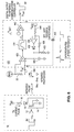
- receiver 1020 of FIG. 10 Yet another embodiment of a receiver circuit suitable for use as integrated receiver 220 is receiver 1020 of FIG. 10.
- receiver 1020 is designed with positive feedback and feedback detection which monitors the feedback transients and prevents signal disable switch 1048 from closing while a feedback transient is present.
- Feedback detect comparator 1060 compares the amplified input data signal at the output of input amplifier 1026 to the detection threshold voltage level V DET and output a high level signal so long as the amplified input signal is greater that the detection threshold.
- Exclusive-OR 1062 compares the output of the feedback detect comparator 1060 with the delayed digital output signal and outputs a high level signal if the two signals differ. Conversely, exclusive-OR 1062 outputs a low level if the two signals are in agreement. This low output signal will propagate through AND gate 1064 to close signal disable switch 1048 before the edge triggered disable signal output from exclusive-OR 1052 would normally cause switch 1048 to close. This permits receiver 1020 to operate at higher speeds when the transient settling time is faster than that predicted solely by the timing of the edge-triggered one shot circuit.
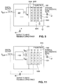
- FIG. 11 shows another embodiment of a photodiode 1230 according to the present invention which can be employed with a receiver 1120 having a pair of differential inputs D IR1 and D IR2 .
- Photodiode 1230 is similar in structure to photodiode 330 of FIG. 3.
- a series of N-diffusions 332 are formed in P-substrate 1210 and interconnected via connection traces 1234 to input terminal D IR1 of receiver 1120.
- An additional set of insulated traces 1238 is formed adjacent the connection traces 1234 and connected to input terminal D IR2 of receiver 1120.
- connection traces 1234 and insulated traces 1238 have the same area, they will each receive the same noise signal which is subsequently cancelled by the differential nature of the receiver 1120. Since the insulated traces 1238 occupy only about 1/50 of the area of the photodiode, they only slightly reduce the light efficiency of the photodiode 330. Because the insulated traces have the same area as connection traces 1234, they will pick up approximately the same magnitude of noise signal. To maximize the differential balance between the connection traces 1234 and the insulated traces 1238, the insulated traces should have the same structure and the connection traces and should be interleaved with the connection traces 1234 as is shown in FIG. 11.
- the receiver circuits 420, 620, 820, 920 and 1020 can each be modified to operate in a differential mode with the photodiodes illustrated in FIG. 11, as should be apparent to one skilled in the art.
Landscapes
- Physics & Mathematics (AREA)
- Electromagnetism (AREA)
- Engineering & Computer Science (AREA)
- Computer Networks & Wireless Communication (AREA)
- Signal Processing (AREA)
- Light Receiving Elements (AREA)
- Optical Communication System (AREA)
- Solid State Image Pick-Up Elements (AREA)
Abstract
Description
Claims (38)
- A distributed photodiode, the photodiode comprising:a substrate, the substrate being doped with a first dopant type and having first and second planar surfaces;a plurality of diffusions, the plurality of diffusions being doped with a second dopant type and formed on the first planar surface of the substrate; anda first plurality of connective traces disposed on the first planar surface of the substrate and coupled to each of the plurality of diffusions.
- The distributed photodiode of claim 1, further including a conductive layer formed on the second planar surface of the substrate.
- The distributed photodiode of claim 1, further including a plurality of conductive shields disposed along the first plurality of connective traces.
- The distributed photodiode of claim 1, wherein each of the plurality of diffusions is a minimum geometry structure for a semiconductor fabrication process.
- The distributed photodiode of claim 4, wherein each of the plurality of connective traces is a minimum width metal trace for the semiconductor fabrication process.
- The distributed photodiode of claim 1, wherein each one of the plurality of diffusions is spaced at a predetermined interval from an adjacent one of the plurality of diffusions.
- The distributed photodiode of claim 6, wherein the predetermined interval is less than an average distance travelled by photo-generated carriers in the substrate before recombination.
- The distributed photodiode of claim 1, further including a second plurality of connective traces disposed on the first planar surface of the substrate and interlineated with the first plurality of connective traces.
- A method for producing a photodiode, the method comprising the steps:providing a substrate having first and second planar surfaces;doping the substrate with a first dopant type;diffusing a second dopant type at a plurality of sites on the first planar surface of the substrate to form a plurality of diffusions; anddisposing a first set of conductive traces on the first surface planar surface to interconnect each of the plurality of diffusions.
- The method of claim 9, further including the step of disposing a first conductive layer on the second planar surface of the substrate.
- The method of claim 9, further including the step of disposing a conductive shield layer adjacent the first set of conductive traces.
- The method of claim 9, wherein the step of diffusing a second dopant type at a plurality of sites on the first planar surface of the substrate to form a plurality of diffusions includes forming the diffusions with a minimum geometry for a semiconductor fabrication process.
- The method of claim 12, wherein the step of disposing a first set of conductive traces on the first surface planar surface to interconnect each of the plurality of diffusions includes forming the conductive traces with a minimum width metal trace for the semiconductor fabrication process.
- The method of claim 9, wherein the step of diffusing a second dopant type at a plurality of sites on the first planar surface of the substrate to form a plurality of diffusions includes the step of uniformly spacing the plurality of diffusions at a predetermined interval from one another, where the predetermined interval is less than an average distance travelled by photo-generated carriers in the substrate before recombination.
- The method of claim 9, further including the step of forming a second plurality of connective traces disposed on the first planar surface of the substrate, wherein the second plurality of connective traces is interleaved with the first plurality of connective traces.
- An integrated photodiode and receiver circuit, the circuit comprising:a substrate, the substrate being doped with a first dopant type and having first and second planar surfaces;a plurality of diffusions, the plurality of diffusions being doped with a second dopant type and formed on the first planar surface of the substrate;a first plurality of connective traces disposed on the first planar surface of the substrate and coupled to each of the plurality of diffusions; anda receiver circuit formed on the substrate, where a first input terminal of the receiver circuit is coupled to the first plurality of connective traces.
- The integrated photodiode and receiver circuit of claim 16, further including a conductive layer formed on the second planar surface of the substrate.
- The integrated photodiode and receiver circuit of claim 17, wherein the receiver circuit further comprises:a receiver output terminal;an input amplifier interposed between the first input and receiver output terminals, the input amplifier being configured to receive and amplify the input signal to produce an amplified input signal, and wherein the input amplifier is further configured to vary the gain of the input amplifier responsive to a gain control signal;a bandpass filter interposed between the input amplifier and the receiver output terminal, the bandpass filter being configured to receive and bandpass filter the amplified input signal so as to produce a filtered input signal;a comparator interposed between the bandpass filter and the receiver output terminal, the comparator being configured to compare the filtered input signal to a detection threshold voltage level in order to generate a digital output signal;a delay circuit interposed between the comparator and the receiver output terminal, the delay circuit being configured to receive the digital output signal and generate a delayed digital output signal responsive thereto;an automatic gain control circuit configured to receive the filtered input signal, the automatic gain control circuit comparing the filtered input signal to an automatic gain control threshold voltage and generating the gain control signal responsive thereto;an isolation control signal generator configured to receive the delayed digital output signal and generating an isolation control signal responsive thereto; andan isolation switch interposed between the input amplifier and the automatic gain control circuit, the isolation switch being configured to receive the isolation control signal and, responsive thereto, isolate the automatic gain control circuit from the amplified input signal.
- The receiver circuit of claim 18 wherein the isolation switch is further configured to isolate the comparator from the amplified input signal responsive to the isolation control signal.
- The receiver circuit of claim 18 wherein the isolation switch is further configured to isolate the bandpass filter from the amplified input signal responsive to the isolation control signal.
- The receiver of claim 18 wherein the isolation control signal generator comprises a one-shot circuit configured to generate an output pulse of a predetermined duration responsive to a falling edge in the delayed digital output signal.
- The receiver of claim 18 wherein the isolation control signal generator comprises an edge triggered one-shot circuit configured to generate an output pulse of a predetermined duration responsive to each edge in the delayed digital output signal.
- The receiver of claim 22 wherein the edge triggered one-shot circuit comprises:a first exclusive-OR gate having first and second input terminals and an output terminal, wherein the first input terminal is configured to receive the delayed digital output signal;a resistor having first and second terminals, wherein the first terminal is configured to receive the delayed digital output signal, and further wherein the second terminal is coupled to the second input terminal of the first exclusive-OR gate; anda capacitor coupled between the second input terminal of the first exclusive-OR gate and ground;whereby the first exclusive-OR gate generates the isolation control signal at its output terminal responsive to the delayed digital output signal.
- The receiver of claim 22 wherein the isolation control signal generator further includes:a feedback detect comparator configured to receive the amplified input signal and compare it to the detection threshold voltage level to produce a feedback detect signal;a second exclusive-OR gate having first and second input terminals and an output terminal, wherein the first input terminal is configured to receive the feedback detect signal and the second input terminal is configured to receive the delayed digital output signal; andan AND gate having first and second input terminals and an output terminal, wherein the first input terminal is coupled to the output terminal of the first exclusive-OR gate and the second input terminal is coupled to the output terminal of the second exclusive-OR gate whereby the AND gate generates the isolation control signal at its output terminal.
- The integrated photodiode and receiver circuit of claim 18, further including a second plurality of connective traces disposed on the first planar surface of the substrate and interlineated with the first plurality of connective traces, and wherein the input amplifier of the receiver circuit is a differential amplifier having a second input terminal coupled to the second plurality of connective traces.
- The receiver circuit of claim 25 wherein the isolation switch is further configured to isolate the comparator from the amplified input signal responsive to the isolation control signal.
- The receiver circuit of claim 25 wherein the isolation switch is further configured to isolate the bandpass filter from the amplified input signal responsive to the isolation control signal.
- The receiver of claim 25 wherein the isolation control signal generator comprises a one-shot circuit configured to generate an output pulse of a predetermined duration responsive to a falling edge in the delayed digital output signal.
- The receiver of claim 25 wherein the isolation control signal generator comprises an edge triggered one-shot circuit configured to generate an output pulse of a predetermined duration responsive to each edge in the delayed digital output signal.
- The receiver of claim 29 wherein the edge triggered one-shot circuit comprises:a first exclusive-OR gate having first and second input terminals and an output terminal, wherein the first input terminal is configured to receive the delayed digital output signal;a resistor having first and second terminals, wherein the first terminal is configured to receive the delayed digital output signal, and further wherein the second terminal is coupled to the second input terminal of the first exclusive-OR gate; anda capacitor coupled between the second input terminal of the first exclusive-OR gate and ground;whereby the first exclusive-OR gate generates the isolation control signal at its output terminal responsive to the delayed digital output signal.
- The receiver of claim 29 wherein the isolation control signal generator further includes:a feedback detect comparator configured to receive the amplified input signal and compare it to the detection threshold voltage level to produce a feedback detect signal;a second exclusive-OR gate having first and second input terminals and an output terminal, wherein the first input terminal is configured to receive the feedback detect signal and the second input terminal is configured to receive the delayed digital output signal; andan AND gate having first and second input terminals and an output terminal, wherein the first input terminal is coupled to the output terminal of the first exclusive-OR gate and the second input terminal is coupled to the output terminal of the second exclusive-OR gate whereby the AND gate generates the isolation control signal at its output terminal.
- The integrated photodiode and receiver circuit of claim 17, wherein the receiver circuit further comprises:an input amplifier having a first input terminal, a gain control terminal and an output terminal, the first input terminal being coupled to the first plurality of connective traces;a bandpass filter having input and output terminals, the input terminal being coupled to the output terminal of the input amplifier;a comparator having first and second input terminals and an output terminal, the first input terminal being configured to receive a detection threshold voltage, the second input terminal being coupled to the output of the bandpass filter, and the output terminal being coupled to an output terminal of the receiver circuit;an automatic gain control circuit having first and second input terminals and an output terminal, the first input terminal being coupled to the output of the bandpass filter, the second input terminal being configured to receive an automatic gain control threshold voltage, and the output terminal being coupled to the gain control terminal of the input amplifier;a delay circuit having input and output terminals, wherein the input terminal is coupled to the output terminal of the comparator such that an output data signal is generated at the output terminal of the delay circuit responsive to the input data signal;an isolation control signal generator having input and output terminals, wherein the input terminal is coupled to the output terminal of the delay circuit, and wherein the isolation control signal generator is configured to generate a pulse of predetermined duration at its output terminal responsive to an edge in the output data signal; andan isolation switch having input, output and control terminals, the control terminal being coupled to the output terminal of the isolation control signal generator such that the isolation switch isolates the input terminal thereof from the output terminal thereof responsive to the automatic gain control signal, the input terminal of the isolation switch being coupled to the output terminal of the input amplifier, the output terminal of the isolation switch being coupled to the first input terminal of the automatic gain control circuit such that the isolation switch is interposed between the first input terminal of the automatic gain control circuit and the output terminal of the input amplifier whereby the isolation switch isolates the automatic gain control circuit from the output terminal of the input amplifier responsive to the isolation control signal.
- The receiver of claim 32 wherein the output terminal of the isolation switch is further coupled to the second input terminal of the comparator such that the isolation switch is interposed between the second input terminal of the comparator and the output terminal of the input amplifier whereby the isolation switch isolates the comparator from the output terminal of the input amplifier responsive to the isolation control signal.
- The receiver of claim 32 wherein the output terminal of the isolation switch is further coupled to the input terminal of the bandpass filter such that the isolation switch is interposed between the input terminal of the bandpass filter and the output terminal of the input amplifier whereby the isolation switch isolates the bandpass filter from the output terminal of the input amplifier responsive to the isolation control signal.
- The receiver of claim 33 wherein the output terminal of the isolation switch is further coupled to the input terminal of the bandpass filter such that the isolation switch is interposed between the input terminal of the bandpass filter and the output terminal of the input amplifier whereby the isolation switch isolates the bandpass filter from the output terminal of the input amplifier responsive to the isolation control signal.
- The receiver of claim 35 wherein the isolation control signal generator comprises a one-shot circuit configured to generate an output pulse of a predetermined duration at the output terminal responsive to a falling edge in the delayed digital output signal.
- The receiver of claim 35 wherein the isolation control signal generator comprises an edge triggered one-shot circuit configured to generate an output pulse of a predetermined duration at the output terminal responsive to each edge in the delayed digital output signal.
- The integrated photodiode and receiver circuit of claim 32, further including a second plurality of connective traces disposed on the first planar surface of the substrate and interlineated with the first plurality of connective traces, and wherein the input amplifier of the receiver circuit is a differential amplifier having a second input terminal coupled to the second plurality of connective traces.
Applications Claiming Priority (2)
| Application Number | Priority Date | Filing Date | Title |
|---|---|---|---|
| US37258 | 1998-03-09 | ||
| US09/037,258 US6198118B1 (en) | 1998-03-09 | 1998-03-09 | Distributed photodiode structure |
Publications (3)
| Publication Number | Publication Date |
|---|---|
| EP0942472A2 true EP0942472A2 (en) | 1999-09-15 |
| EP0942472A3 EP0942472A3 (en) | 2002-10-16 |
| EP0942472B1 EP0942472B1 (en) | 2009-09-16 |
Family
ID=21893354
Family Applications (1)
| Application Number | Title | Priority Date | Filing Date |
|---|---|---|---|
| EP99200543A Expired - Lifetime EP0942472B1 (en) | 1998-03-09 | 1999-02-25 | Distributed photodiode and integrated circuit comprising said photodiode and an infrared receiver |
Country Status (4)
| Country | Link |
|---|---|
| US (1) | US6198118B1 (en) |
| EP (1) | EP0942472B1 (en) |
| JP (1) | JPH11298033A (en) |
| DE (1) | DE69941412D1 (en) |
Cited By (4)
| Publication number | Priority date | Publication date | Assignee | Title |
|---|---|---|---|---|
| WO2001088989A3 (en) * | 2000-05-18 | 2002-06-06 | Raytheon Co | Unit cell with fan-out for large focal plane arrays with small detector pitch |
| EP1241710A3 (en) * | 2001-03-15 | 2006-01-18 | Philips Intellectual Property & Standards GmbH | Light-sensitive semiconductor device |
| DE102005005049A1 (en) * | 2005-02-03 | 2006-08-10 | Siemens Ag | Communication-capable motor starter |
| EP2988164A1 (en) * | 2014-08-21 | 2016-02-24 | Renesas Electronics Corporation | Optical semiconductor device |
Families Citing this family (14)
| Publication number | Priority date | Publication date | Assignee | Title |
|---|---|---|---|---|
| JP2960560B2 (en) * | 1991-02-28 | 1999-10-06 | 株式会社日立製作所 | Microelectronic equipment |
| US6753586B1 (en) | 1998-03-09 | 2004-06-22 | Integration Associates Inc. | Distributed photodiode structure having majority dopant gradient and method for making same |
| DE19835263C2 (en) * | 1998-08-04 | 2000-06-21 | Siemens Ag | Integrated circuit with electrical connections that can be separated by the action of energy |
| FR2791474B1 (en) * | 1999-03-26 | 2001-06-08 | Centre Nat Rech Scient | SEMICONDUCTOR INFRARED DETECTOR AND ITS MANUFACTURING METHOD |
| JP2002217447A (en) * | 2001-01-16 | 2002-08-02 | Toshiba Corp | Semiconductor light receiving device and semiconductor receiving and transmitting system |
| JP3807954B2 (en) | 2001-06-25 | 2006-08-09 | シャープ株式会社 | Photodiode |
| FR2933535B1 (en) * | 2008-07-04 | 2011-03-18 | France Etat | ELECTRONIC DEVICE COMPRISING A PLURALITY OF ELECTRONIC COMPONENTS REPORTED ON A SUBSTRATE AND INFRARED SENSOR THEREFOR |
| KR101239134B1 (en) * | 2008-12-10 | 2013-03-07 | 한국전자통신연구원 | Optical loss modulator and manufacturing method thereof |
| JP5091886B2 (en) | 2009-02-13 | 2012-12-05 | 浜松ホトニクス株式会社 | Image sensor |
| JP5271104B2 (en) * | 2009-02-13 | 2013-08-21 | 浜松ホトニクス株式会社 | Linear image sensor |
| US8384559B2 (en) | 2010-04-13 | 2013-02-26 | Silicon Laboratories Inc. | Sensor device with flexible interface and updatable information store |
| CN102355215B (en) * | 2011-05-20 | 2013-10-02 | 武汉艾立卡电子有限公司 | Non-contact audio equipment volume controller and control method thereof |
| US8837934B2 (en) * | 2011-08-30 | 2014-09-16 | Avago Technologies General Ip (Singapore) Pte. Ltd. | Monitoring circuitry for optical transceivers |
| US11239805B2 (en) * | 2018-10-09 | 2022-02-01 | Analog Devices, Inc. | Differential opto isolator |
Family Cites Families (15)
| Publication number | Priority date | Publication date | Assignee | Title |
|---|---|---|---|---|
| US3377215A (en) * | 1961-09-29 | 1968-04-09 | Texas Instruments Inc | Diode array |
| US3437890A (en) * | 1963-05-10 | 1969-04-08 | Ibm | Diffused-epitaxial scanistors |
| FR1552078A (en) * | 1967-11-15 | 1969-01-03 | ||
| GB1206308A (en) * | 1967-11-22 | 1970-09-23 | Sony Corp | Method of making semiconductor wafer |
| US3539875A (en) * | 1968-09-25 | 1970-11-10 | Philips Corp | Hardware envelope with semiconductor mounting arrangements |
| US3638026A (en) * | 1970-06-29 | 1972-01-25 | Honeywell Inc | Or photovoltaic device |
| US3676741A (en) * | 1970-12-09 | 1972-07-11 | Bell Telephone Labor Inc | Semiconductor target structure for image converting device comprising an array of silver contacts having discontinuous nodular structure |
| US3882532A (en) * | 1972-07-03 | 1975-05-06 | Ibm | Externally accessing mechanically difficult to access circuit nodes in integrated circuits |
| GB2095905B (en) * | 1981-03-27 | 1985-01-16 | Philips Electronic Associated | Infra-red radiation imaging devices and methods for their manufacture |
| US5243215A (en) * | 1990-05-31 | 1993-09-07 | Fuji Electric Co., Ltd. | Semiconductor photodiode device with reduced junction area |
| US5646437A (en) * | 1991-08-08 | 1997-07-08 | Santa Barbara Research Center | Indium antimonide (InSb) photodetector device and structure for infrared, visible and ultraviolet radiation |
| CA2070708C (en) * | 1991-08-08 | 1997-04-29 | Ichiro Kasai | Visible and infrared indium antimonide (insb) photodetector with non-flashing light receiving surface |
| US5633526A (en) * | 1992-11-01 | 1997-05-27 | Rohm Co., Ltd. | Photodiode array and method for manufacturing the same |
| US5329115A (en) * | 1993-04-29 | 1994-07-12 | International Business Machines Corporation | Optical receiver circuit |
| US5821567A (en) * | 1995-12-13 | 1998-10-13 | Oki Electric Industry Co., Ltd. | High-resolution light-sensing and light-emitting diode array |
-
1998
- 1998-03-09 US US09/037,258 patent/US6198118B1/en not_active Expired - Lifetime
-
1999
- 1999-02-25 EP EP99200543A patent/EP0942472B1/en not_active Expired - Lifetime
- 1999-02-25 DE DE69941412T patent/DE69941412D1/en not_active Expired - Lifetime
- 1999-03-09 JP JP11062291A patent/JPH11298033A/en active Pending
Cited By (5)
| Publication number | Priority date | Publication date | Assignee | Title |
|---|---|---|---|---|
| WO2001088989A3 (en) * | 2000-05-18 | 2002-06-06 | Raytheon Co | Unit cell with fan-out for large focal plane arrays with small detector pitch |
| EP1241710A3 (en) * | 2001-03-15 | 2006-01-18 | Philips Intellectual Property & Standards GmbH | Light-sensitive semiconductor device |
| DE102005005049A1 (en) * | 2005-02-03 | 2006-08-10 | Siemens Ag | Communication-capable motor starter |
| EP2988164A1 (en) * | 2014-08-21 | 2016-02-24 | Renesas Electronics Corporation | Optical semiconductor device |
| US9508662B2 (en) | 2014-08-21 | 2016-11-29 | Renesas Electronics Corporation | Optical semiconductor device |
Also Published As
| Publication number | Publication date |
|---|---|
| JPH11298033A (en) | 1999-10-29 |
| US6198118B1 (en) | 2001-03-06 |
| DE69941412D1 (en) | 2009-10-29 |
| EP0942472A3 (en) | 2002-10-16 |
| EP0942472B1 (en) | 2009-09-16 |
Similar Documents
| Publication | Publication Date | Title |
|---|---|---|
| US6356375B1 (en) | Apparatus and method for an integrated photodiode in an infrared receiver | |
| US6556330B2 (en) | Apparatus and method for an integrated photodiode in an infrared receiver | |
| EP0942472B1 (en) | Distributed photodiode and integrated circuit comprising said photodiode and an infrared receiver | |
| US6181454B1 (en) | Adaptive threshold controlled decision circuit immune to ringing components of digital signals | |
| US9621279B2 (en) | Optical receiver circuit | |
| US6240283B1 (en) | Apparatus and method for feedback mitigation in a low speed communications receiver | |
| EP3387680B1 (en) | Avalanche photodetectors | |
| WO2016175828A1 (en) | Monolithically integrated photodetector and receiver | |
| Forrest | Optical detectors: Three contenders: Depending on the application, the photoeonductor, pin diode, or avalanche photodiode may prove the best choice | |
| Ray et al. | Speed optimized large area avalanche photodetector in standard CMOS technology for visible light communication | |
| Hartman et al. | A monolithic silicon photodetector/amplifier IC for fiber and integrated optics application | |
| US6753586B1 (en) | Distributed photodiode structure having majority dopant gradient and method for making same | |
| US20060108657A1 (en) | Photodiode detector | |
| US5136346A (en) | Photon stimulated variable capacitance effect devices | |
| US5130526A (en) | Circuit array for optical schmitt trigger | |
| EP0877426B1 (en) | A method for shortening the time response of a radiation detector and a detector using that method | |
| US6548878B1 (en) | Method for producing a thin distributed photodiode structure | |
| Brain et al. | Phototransistors, APD-FET, and PINFET optical receivers for 1-1.6-µm wavelength | |
| Chukwujekwu et al. | Technical report: comparative analysis of photodetectors for appropriate usage in optical communication applications | |
| Takano et al. | Monolithic integration of 5-Gb/s optical receiver block for short distance communication | |
| JPH1050967A (en) | Light receiving operation element | |
| CN114497003A (en) | Surface incident photodiode structure with dark current self-compensation function | |
| Tsaur et al. | A nondirective infrared transceiver for indoor high speed wireless data communication | |
| EP3683837A1 (en) | Optical sensor and apparatus comprising an optical sensor | |
| KR102672313B1 (en) | Light-receiving device having electromagnetic interference removal function |
Legal Events
| Date | Code | Title | Description |
|---|---|---|---|
| PUAI | Public reference made under article 153(3) epc to a published international application that has entered the european phase |
Free format text: ORIGINAL CODE: 0009012 |
|
| AK | Designated contracting states |
Kind code of ref document: A2 Designated state(s): AT BE CH CY DE DK ES FI FR GB GR IE IT LI LU MC NL PT SE |
|
| AX | Request for extension of the european patent |
Free format text: AL;LT;LV;MK;RO;SI |
|
| RIN1 | Information on inventor provided before grant (corrected) |
Inventor name: HOLCOMBE, WAYNE THOMAS |
|
| PUAL | Search report despatched |
Free format text: ORIGINAL CODE: 0009013 |
|
| RIC1 | Information provided on ipc code assigned before grant |
Free format text: 7H 01L 31/103 A, 7H 01L 27/144 B, 7H 04B 10/158 B, 7H 01L 31/0352 B, 7H 01L 31/02 B |
|
| AK | Designated contracting states |
Kind code of ref document: A3 Designated state(s): AT BE CH CY DE DK ES FI FR GB GR IE IT LI LU MC NL PT SE |
|
| AX | Request for extension of the european patent |
Free format text: AL;LT;LV;MK;RO;SI |
|
| 17P | Request for examination filed |
Effective date: 20030214 |
|
| AKX | Designation fees paid |
Designated state(s): DE FR GB |
|
| GRAP | Despatch of communication of intention to grant a patent |
Free format text: ORIGINAL CODE: EPIDOSNIGR1 |
|
| RIC1 | Information provided on ipc code assigned before grant |
Ipc: H01L 31/02 20060101ALI20090302BHEP Ipc: H01L 31/0352 20060101ALI20090302BHEP Ipc: H04B 10/158 20060101ALI20090302BHEP Ipc: H01L 31/103 20060101AFI20090302BHEP |
|
| GRAS | Grant fee paid |
Free format text: ORIGINAL CODE: EPIDOSNIGR3 |
|
| GRAA | (expected) grant |
Free format text: ORIGINAL CODE: 0009210 |
|
| AK | Designated contracting states |
Kind code of ref document: B1 Designated state(s): DE FR GB |
|
| REG | Reference to a national code |
Ref country code: GB Ref legal event code: FG4D |
|
| REF | Corresponds to: |
Ref document number: 69941412 Country of ref document: DE Date of ref document: 20091029 Kind code of ref document: P |
|
| RAP2 | Party data changed (patent owner data changed or rights of a patent transferred) |
Owner name: SILICON LABORATORIES INC. |
|
| PLBE | No opposition filed within time limit |
Free format text: ORIGINAL CODE: 0009261 |
|
| STAA | Information on the status of an ep patent application or granted ep patent |
Free format text: STATUS: NO OPPOSITION FILED WITHIN TIME LIMIT |
|
| 26N | No opposition filed |
Effective date: 20100617 |
|
| GBPC | Gb: european patent ceased through non-payment of renewal fee |
Effective date: 20100225 |
|
| REG | Reference to a national code |
Ref country code: FR Ref legal event code: ST Effective date: 20101029 |
|
| PG25 | Lapsed in a contracting state [announced via postgrant information from national office to epo] |
Ref country code: FR Free format text: LAPSE BECAUSE OF NON-PAYMENT OF DUE FEES Effective date: 20100301 |
|
| PG25 | Lapsed in a contracting state [announced via postgrant information from national office to epo] |
Ref country code: GB Free format text: LAPSE BECAUSE OF NON-PAYMENT OF DUE FEES Effective date: 20100225 |
|
| PGFP | Annual fee paid to national office [announced via postgrant information from national office to epo] |
Ref country code: DE Payment date: 20110223 Year of fee payment: 13 |
|
| REG | Reference to a national code |
Ref country code: DE Ref legal event code: R119 Ref document number: 69941412 Country of ref document: DE Effective date: 20120901 |
|
| PG25 | Lapsed in a contracting state [announced via postgrant information from national office to epo] |
Ref country code: DE Free format text: LAPSE BECAUSE OF NON-PAYMENT OF DUE FEES Effective date: 20120901 |