EP0940046B1 - Processor for signaling messsages in a data switching network - Google Patents
Processor for signaling messsages in a data switching network Download PDFInfo
- Publication number
- EP0940046B1 EP0940046B1 EP97946492A EP97946492A EP0940046B1 EP 0940046 B1 EP0940046 B1 EP 0940046B1 EP 97946492 A EP97946492 A EP 97946492A EP 97946492 A EP97946492 A EP 97946492A EP 0940046 B1 EP0940046 B1 EP 0940046B1
- Authority
- EP
- European Patent Office
- Prior art keywords
- message
- switch
- processing unit
- messages
- signaling
- Prior art date
- Legal status (The legal status is an assumption and is not a legal conclusion. Google has not performed a legal analysis and makes no representation as to the accuracy of the status listed.)
- Expired - Lifetime
Links
Images

Classifications
-
- H—ELECTRICITY
- H04—ELECTRIC COMMUNICATION TECHNIQUE
- H04Q—SELECTING
- H04Q3/00—Selecting arrangements
- H04Q3/42—Circuit arrangements for indirect selecting controlled by common circuits, e.g. register controller, marker
- H04Q3/54—Circuit arrangements for indirect selecting controlled by common circuits, e.g. register controller, marker in which the logic circuitry controlling the exchange is centralised
- H04Q3/545—Circuit arrangements for indirect selecting controlled by common circuits, e.g. register controller, marker in which the logic circuitry controlling the exchange is centralised using a stored program
- H04Q3/54575—Software application
- H04Q3/54583—Software development, e.g. procedural, object oriented, software generation, software testing
-
- H—ELECTRICITY
- H04—ELECTRIC COMMUNICATION TECHNIQUE
- H04Q—SELECTING
- H04Q3/00—Selecting arrangements
- H04Q3/0016—Arrangements providing connection between exchanges
- H04Q3/0025—Provisions for signalling
-
- H—ELECTRICITY
- H04—ELECTRIC COMMUNICATION TECHNIQUE
- H04Q—SELECTING
- H04Q2213/00—Indexing scheme relating to selecting arrangements in general and for multiplex systems
- H04Q2213/13056—Routines, finite state machines
Definitions
- a CPU 88 which is preferably a Motorola 68EC040 microprocessor, is connected in communicating relationship with primary and secondary HDLC buses 50a and 50b, respectively, as well as a timing and control unit 78, a buffer 84, an internal-bus arbiter 86, a read only memory (ROM) 90 containing the operating system for the card 38 and a random access memory (RAM) 92 containing applications software described below.
- a battery 94 provides backup power for RAM 92 so that information stored therein is preserved in the event of an interruption of the primary power supply (not shown).
- the SS7 card 38 receives outgoing messages from, and sends incoming messages to, the CPU/matrix card or nodal switch 44a over the HDLC bus 50a.
Landscapes
- Engineering & Computer Science (AREA)
- Computer Networks & Wireless Communication (AREA)
- Data Exchanges In Wide-Area Networks (AREA)
- Telephonic Communication Services (AREA)
- Communication Control (AREA)
- Exchange Systems With Centralized Control (AREA)
Abstract
Description
- This invention relates to a signaling unit for the control of digital communications transmitted over a switching network. More specifically, it relates to a signaling unit having a variable signaling-message repertoire used in setting up and releasing communications channels in a digital switched network such as ISDN, and also in performing various maintenance functions in the network and providing enhanced subscriber services.
- The invention will be described in connection with a data network in which signaling messages are transmitted over a signaling channel and data, including digitized voice signals, are transmitted over a "CIC" channel. Access signaling is governed by a standard suite of protocols known as Signaling System No. 7 (SS7) which defines the various signaling messages, including their formats, used in call-setup and release and various other control functions. A description of SS7 is set forth in Madrases, et al., An Overview of Signaling System No. 7, Proceedings of the IEEE, Vol. 80, No. 4, April 1992. While SS7 provides a fairly extensive repertoire of signaling messages, it is often desirable to augment the message set with additional messages. For example, it may be desirable to provide subscriber services that are unavailable with the standard message set.
- Moreover, the requirements for additional messages will vary from one network to another and it is therefore impractical to provide each Service Switching Point (SSP) with the ability to deal with all of the possible message types. Furthermore, the requirements for additional message types at any given SSP may vary from time to time. Accordingly, it is desirable to provide a system in which the message repertoire of an SSP can be initially determined and also changed from time to time, in the field, ideally by the operator of the switching system.
- A signaling system embodying the invention includes, at each SSP, a signaling unit containing a message configuration template containing an entry for each type of message. Each entry contains the complete format for the corresponding message type. For incoming messages, the signaling unit also includes, for each voice channel (CIC) multiple finite state machines which manage operations associated with each of the message types that are involved in CIC control. When a message is received, the message type field in the message is used to identify the message type and invoke the operation of the associated state machine. The state machine then parses the message and performs the operations required by the message.
- For example, if the incoming message is an Initial Address Message (IAM) used by a remote SSP in setting up a call to a subscriber linked with the local SSP, the associated state machine parses the message and passes to the local switch matrix various parameters contained in the message. These include, for example, the telephone number of the called subscriber and the number of the remote subscriber who initiated the call. Based on criteria contained in the switch matrix and/or host computer communications software, e.g., whether the line to the called subscriber is busy, the matrix communicates the appropriate response to the signaling unit. The signaling unit in turn accesses the message configuration template for the template corresponding to the outgoing message, formats a message according to that template and transmits the message to the call-originating SSP.
- The state machines are in the form of software routines executed by a central processing unit (CPU) in the signaling unit. These routines and the message configuration template are situated in a random access memory (RAM) in the unit. Accordingly, the user can easily add to the message repertoire by making a corresponding entry in the message configuration template and writing the software routine for the corresponding state machine. Similarly, the programming of a state machine can be simplified by means of a high-level language whose primitives invoke combinations of low-level processor functions directed to the operations of a state machine in the environment of the invention. An arrangement of this kind is described in U.S. Patent No. 5,546,453.
- The message configuration template also permits screening of incoming messages to make sure that their contents are consistent with the specified formats of those messages. A state machine that is configured to perform this task can reject messages that do not meet the specified criteria therefor and, in turn, return appropriate messages to the STP's that originated the faulty messages.
-
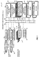
- Fig. 1 is a diagram of a digital switch containing a signaling system incorporating the invention;
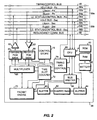
- Fig. 2 is a diagram of a signaling unit incorporating the invention, included in the switch of Fig. 1;
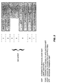
- Fig. 3 is a diagram of the protocol stack used in transmitting signaling messages processed by the signaling unit of Fig 2;
- Fig. 4 is a diagram of the message processing procedure performed by the signaling unit; and
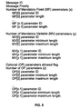
- Fig. 5 is a list of the fields contained in a template in the message configuration table shown in Fig. 4.
-
- Figure 1 illustrates an environment in which the present invention may operate. A
programmable telecommunications switch 2 includes network/line interfaces 4, each of which may represent a link to a public switched telephone network (PSTN) or private network or a subscriber line. These interfaces are provided on a series of input/output (IO)cards 20. - One or more digital network (T1, E1, or J1) or analog trunk/
line line cards 26 communicate with theIO cards 20 over a linecard IO bus 28. Theline cards 26 are also connected in communicating relationship withredundant switching buses redundant IO card 22 and redundant IO bus 24 may optionally be provided to permit continued operation of the switch in the event of a failure of one ofIO cards 20. Again, if desired, one or moreredundant line cards 32 may be provided, such redundant line cards arranged to communicate with aredundant IO card 22 over redundantLC IO lines 34. It should be understood that by providing other types of cards within theswitch 2, other types of communication protocols such as DS3, SONET or others may also be supported by the switch. - Control of the operations of the
switch 2, as well as the actual switching functions, are performed by a CPU/matrix card ornodal switch 44a sometimes referred to as "card/switch" hereinafter. If a CPU/matrix card is selected, theswitch 2 will operate as a standalone device (i.e., as opposed to operating as a switching node in an expandable telecommunications system). In that case, the CPU/matrix card 44a is connected to ahost interface 42a through which communications with an external host device (not shown) are effected. - Alternatively, if a nodal switch is selected, the
switch 2 may operate as a switching node in an expandable switching system. In such an embodiment, the nodal switch is preferably connected with aring IO card 40a through which communications with a pair of fiberoptic rings 12a are effected. The nodal switch may also communicate with an external host via thehost interface 42a. - Regardless of whether a CPU/matrix card or a nodal switch is selected, a matching standby a CPU/matrix card or
nodal switch 44b may optionally be provided and accompanied by theappropriate host interface 42b orring IO card 40b (or both). In such a configuration, alink 46 is provided for direct communication between active andstandby devices - Details of the construction and operation of a suitable CPU/matrix card may be found in U.S. Patent 5,349,579. Similarly, details of the construction and operation of a suitable nodal switch may be found in U.S. Patent 5,544,163.
- Diverse, programmable communications services such as tone detection and generation, conferencing, voice recorded announcements, call progress analysis, speech recognition, ADPCM compression and many others may be provided by one or more multifunction digital signal processing (MFDSP)
cards 36. SS7 signaling functions are provided by signaling units carried on one ormore SS7 cards 38 incorporating the present invention. Redundant MFDSPcards 36 andredundant SS7 cards 38 may also be included. - Figure 2 is a block diagram of an
SS7 card 38. Bus driver andreceiver LSpcm 52a andSLpcm 54a, in thebus 30a.LSpcm 52a carries pulse coded modulation information in a direction from the line cards 26 (Fig. 1) to the card/switch 44a, the MFDSPcards 36 and theSS7 cards 38. Conversely, theSLpcm 54a path carries PCM information in a direction from card/switch 44a, MFDSPcards 36 andSS7 cards 38 toline cards 26. In a preferred embodiment, two eight-bit parallel buses are used for theLSpcm 52a andSLpcm 54a, respectively. Alternatively, those paths may be implemented by a plurality of multiplexed serial buses, each of which carries a plurality of time slots. It should be understood that other types and configurations of buses may be used to establish appropriate communications between the various cards. - Preferably,
paths - A
CPU 88, which is preferably a Motorola 68EC040 microprocessor, is connected in communicating relationship with primary andsecondary HDLC buses control unit 78, abuffer 84, an internal-bus arbiter 86, a read only memory (ROM) 90 containing the operating system for thecard 38 and a random access memory (RAM) 92 containing applications software described below. Abattery 94 provides backup power forRAM 92 so that information stored therein is preserved in the event of an interruption of the primary power supply (not shown). TheSS7 card 38 receives outgoing messages from, and sends incoming messages to, the CPU/matrix card ornodal switch 44a over theHDLC bus 50a. - A transmit
PCM bank 64 is connected in communicating relationship withbus drivers 60. Similarly, a receive PCM bank is connected in communicating relationship withbus receivers 62. Each ofPCM banks control store 74 as well as to atime slot counter 72. A multiplexer 68, which is also connected totime slot counter 72, is arranged to pass PCM information bidirectionally betweenPCM banks packet engine 70, on the other hand, which assembles incoming and outgoing message packets. A buffer 80 is connected topacket engine 70, a sharedRAM 82 and theinternal bus arbiter 86. - When programmed in an appropriate fashion, the
SS7 card 38 may function as an SS7 server for up to 16 SS7 signaling links as well as management of up to 2048 voice channels (CICs). The timing andcontrol unit 78 receives system timing signals from a timing/control bus 48 to synchronize operations of theSS7 card 38 to a system clock. Thus the timing andcontrol unit 78 provides timing signals to thetime slot counter 72 to time the transmission and reception of signals on thebuses counter 72 also provides signals to thecontrol store 74. - In accordance with a well-known switching arrangement, the
bus paths switch 2, there is a corresponding time slot on thepaths PCM banks control store 74 receive frompath 52a and transmit overpath 54a in the time slots corresponding with the signaling-message channels associated with thecard 38. - The
packet engine 70 assembles the signaling-message portions received in each channel and senses when a complete message has been assembled. It then forwards the message to the buffer 80, from which the message passes to the sharedRAM 82. The CPU 8 accesses the message in theRAM 82 and processes it in accordance with software contained in theRAM 92. - When the
switch 2 is initialized, thecontrol store 74 is loaded with time slot information in accordance with the channels assigned to thecard 38. Also, theRAM 92 is loaded with the software used in processing signaling messages. - More specifically, the messages which the invention processes are in the "integrated services digital network (ISDN) user part" (ISUP) part of the SS7 signaling protocol. As shown in Fig. 3, the protocol includes, inter alia an MTP2 level, which is the data link level, and an MPT3 level, which is part of the network level in the protocol. The ISUP portion of the protocol corresponds to a portion of the network level and also to the transport and application levels.
- As shown in Fig. 4, the software in
RAM 92 containsMTP level state machines 96, amessage configuration template 100, an incomingmessage validation unit 102, an incoming message statemachine event generator 104 and incoming-message translation unit 106, all of which are used in processing incoming messages. Outgoing messages are processed by a validation andtranslation unit 108 in accordance with the appropriate entries contained in themessage configuration template 100 and byMTP levels state machine 104 is located inRAM 92, as are theunits - The
message configuration template 100 includes a template for each type of signaling message as shown in Fig. 4. With reference to Figs. 4 and 5, each template includes: an index number (IDX); the message role; the message type; the number of mandatory fixed parameters and for each of such parameters, the parameter identification (ID) and the parameter length; the number of mandatory variable parameters and for each of those the parameter, ID the parameter minimum length and the parameter maximum length. The template also includes an optional-parameter indicator flag which, if it has a value of one, indicates that one or more optional parameters may be included. In that case the flag is followed by the number of optional parameters and, for each of the optional parameters, the parameter ID, the minimum length of the parameter and the maximum length of the parameter. - The four message types depicted in the
template 100 are an IAM incoming message used in requesting a call set-up; an ACM message which is an address complete message returned to the originator of the IAM message; an ANM message which is an answered message that is returned to the IAM originator when the call is answered; and an REL message which is sent to release the CIC used in the call. - With further reference to Fig. 4, an incoming message is first processed by the
MTP levels state machines 96, and the resulting ISUP message is processed by thevalidation unit 102, which uses the type contained in the message to access thetemplate 100 to obtain the corresponding format entry. It then compares the message with the entry to see if it has a valid format according to the retrieved format entry. - If the format is valid, the
validation unit 102 passes the message to the incoming message statemachine event generator 104. A single state machine may be used to parse several related messages such as the call setup messages. Accordingly, thegenerator 104 invokes the state machine routine to be used in parsing the message. Assuming that the message is one to which the card/switch 44a should respond, theevent generator 104 selects the appropriate state machine for thetranslator 106 and generates an "event", i.e., invokes the appropriate routines in theunit 106 in accordance with the message type. The translation unit parses the message in accordance with the corresponding entry in thetemplate 100 and translates it into a standard form used by the card/switch 44a in connection with all of the calls handled by theswitch 2. The translated message is then forwarded to the card/switch 44a over theHDLC bus 50a. - If the incoming message does not fit the format specified in the
template 100 an appropriate response is generated by aresponse generator 110 and passed to the packet engine 70 (Fig. 2) for transmission back to the message originator. - Outgoing messages received from the card/
switch 44a are passed to the outgoing message validation andtranslation unit 108, which is a state machine that converts the message into appropriate fields of an SS7 message, assembles the fields in accordance with the appropriate entry in thetemplate 100 and passes the messages toMTP levels packet engine 70 for transmission to the SSP at the other end of the message channel. - The various devices depicted in Fig. 4 and, in particular, the
state machines message configuration template 100 are downloaded to theRAM 92 from the card/switch 44a by means of messages sent over the HDLC bus 50. - In addition to the standard SS7 protocol messages, the host may download configuration templates and corresponding state machines for other messages which may be desired by the system operation. These messages for example, may be used in providing various subscriber services such as call transfer. While the user can program these additions or modifications directly in the assembly language of the CPU 88 (Fig. 2), we prefer to use a higher level programming arrangement such as described in U.S. patent 5,546,453.
- It will thus be seen that I have provided a highly flexible signal-message processor that can be configured in the field to handle any desired message repertoire, i.e., both messages specified in a standard such as SS7 and messages specific to the operator's switching system.
- In a preferred embodiment of the invention, message processing is performed in a processing unit on a separate card plugged into a digital switch. Configuration of the unit can then be accomplished at a system console that is used to program other units in the switch. Changes in the message repertoire are readily effected by means of entries into a message configuration template located in a memory in the message processing unit and by modifications to, or additions to, a set of state machines, located in the memory.
- It will be apparent that various modifications can be made to the signaling-message processor described above without departing from the scope of the invention.
Claims (6)
- A message processing unit (38) for processing signaling messages in a digital switch contained in a switching system, said message processing unit comprising;A. a central processor (88)B. a random access memory (92)C. a message configuration template contained in said memory, said configuration template containing a format template for each message type that can be processed by the unit,D. a plurality of state machines (96) contained in said memory and run by said processor, each state machine1. corresponding to one of said message types,2. parsing incoming messages of that type received from sources external to said switch and3. generating an event as a result of said parsing,E. means external to said unit for loading the message configuration template and said state machines into said random access memory, whereby the repertoire of incoming messages that can be processed by the message processing unit can be readily modified or augmented by the operator of said switch.
- The message processing unit defined in Claim 1 further includingA. a translator (106) for translating the parsed messages into a common language used by other elements of the switching system and;B. means for transmitting the translated messages to another element in the system.
- The message processing unit defined in Claim 1 further including;A. an outgoing-message translator (108) that1. translates a signaling message received from another unit in said switch to a form compatible with an entry in said message configuration table, and2. assembles the message in accordance with a template in said table corresponding to the type of said message; andB. means for transmitting the assembled message to a recipient external to said switch.
- A digital switch (2) comprising a switch unit (44a), line cards (26), a signal-message processing unit (38) for conveying signaling messages to and from devices external to said switch and bus means (30a, 30b) providing interconnection of said switch unit, said line cards and said signal-message processing unit, said switch being characterized in that said signal-message processing unit comprises:A. a central processor (88);B. a random access memory (92);C. a message configuration template contained in said memory, said configuration template containing a format template for each message type that can be processed by the processing unit;D. a plurality of state machines (96) contained in said memory and run by said processor, each state machine;1. corresponding to at least one of said message types;2. parsing incoming messages of that type received from sources external to said switch; and3. generating an event as a result of said parsing;E. means external to said unit for loading the message configuration template and said state machines into said random access memory, whereby the repertoire of incoming messages that can be processed by the message processing unit can be readily modified or augmented by the operator of said switching system.
- The switch defined in claim 4 in which said message processing unit further includes:A. a translator (106) for translating the parsed messages into a common language used by other elements of the switch; andB. means for transmitting the translated messages to another element in the system.
- The switch defined in claim 4 in which said message processing unit further includes:A. an outgoing-message translator (108) that1. translates each signaling message received from another unit in said switch to a form compatible with an entry in said message configuration table; and2. assembles the message in accordance with a template in said table corresponding to the type of said message; andB. means for transmitting the assembled message to a recipient external to said switch.
Applications Claiming Priority (3)
| Application Number | Priority Date | Filing Date | Title |
|---|---|---|---|
| US08/754,231 US5987035A (en) | 1996-11-20 | 1996-11-20 | Process for signaling messages in a data switching network |
| US754231 | 1996-11-20 | ||
| PCT/US1997/020031 WO1998023097A1 (en) | 1996-11-20 | 1997-11-04 | Processor for signaling messsages in a data switching network |
Publications (2)
| Publication Number | Publication Date |
|---|---|
| EP0940046A1 EP0940046A1 (en) | 1999-09-08 |
| EP0940046B1 true EP0940046B1 (en) | 2002-04-24 |
Family
ID=25033958
Family Applications (1)
| Application Number | Title | Priority Date | Filing Date |
|---|---|---|---|
| EP97946492A Expired - Lifetime EP0940046B1 (en) | 1996-11-20 | 1997-11-04 | Processor for signaling messsages in a data switching network |
Country Status (9)
| Country | Link |
|---|---|
| US (1) | US5987035A (en) |
| EP (1) | EP0940046B1 (en) |
| JP (1) | JP2001505379A (en) |
| CN (1) | CN1193859A (en) |
| AT (1) | ATE216825T1 (en) |
| AU (1) | AU717670B2 (en) |
| CA (1) | CA2271269C (en) |
| DE (1) | DE69712220T2 (en) |
| WO (1) | WO1998023097A1 (en) |
Families Citing this family (11)
| Publication number | Priority date | Publication date | Assignee | Title |
|---|---|---|---|---|
| US6810031B1 (en) | 2000-02-29 | 2004-10-26 | Celox Networks, Inc. | Method and device for distributing bandwidth |
| US6826175B1 (en) * | 2000-03-31 | 2004-11-30 | Alcatel | Signaling link interface for processing signaling information in a telecommunications network |
| US7218613B1 (en) | 2000-06-30 | 2007-05-15 | Verizon Services Corp | Method and apparatus for in context mediating common channel signaling messages between networks |
| US7184538B1 (en) * | 2000-06-30 | 2007-02-27 | Verizon Services Corp. | Method of and apparatus for mediating common channel signaling message between networks using control message templates |
| US7224686B1 (en) | 2000-06-30 | 2007-05-29 | Verizon Services Corp. | Method of and apparatus for mediating common channel signaling messages between networks using a pseudo-switch |
| US7360090B1 (en) | 2000-06-30 | 2008-04-15 | Verizon Services Corp. | Method of and apparatus for authenticating control messages in a signaling network |
| US6985968B1 (en) | 2001-05-11 | 2006-01-10 | Alcatel | State machine architecture partitionable into control and data planes |
| EP1529387A4 (en) * | 2002-08-14 | 2010-07-14 | Qualcomm Inc | Core network interoperability in a pico cell system |
| DE102004002452B4 (en) * | 2004-01-16 | 2006-07-13 | Siemens Ag | Circuit arrangement and method for error analysis |
| CN100358302C (en) * | 2004-12-06 | 2007-12-26 | 华为技术有限公司 | Method for testing network element interface by state apparatus |
| US12138792B2 (en) * | 2020-03-04 | 2024-11-12 | Fanuc America Corporation | Dynamic messaging system for factory automation device |
Family Cites Families (7)
| Publication number | Priority date | Publication date | Assignee | Title |
|---|---|---|---|---|
| US5392328A (en) * | 1993-02-04 | 1995-02-21 | Bell Communications Research, Inc. | System and method for automatically detecting root causes of switching connection failures in a telephone network |
| US5426694A (en) * | 1993-10-08 | 1995-06-20 | Excel, Inc. | Telecommunication switch having programmable network protocols and communications services |
| US5586177A (en) * | 1995-09-06 | 1996-12-17 | Bell Atlantic Network Services, Inc. | Intelligent signal transfer point (ISTP) |
| WO1996016517A1 (en) * | 1994-11-22 | 1996-05-30 | Unisys Corporation | Extracting and processing data derived from a common channel signalling network |
| KR0136501B1 (en) * | 1994-12-21 | 1998-07-01 | 양승택 | Control Method of Signal Relay Switch Operation Management System |
| US5592530A (en) * | 1995-01-25 | 1997-01-07 | Inet, Inc. | Telephone switch dual monitors |
| US5574782A (en) * | 1995-04-14 | 1996-11-12 | Lucent Technologies Inc. | Minimizing service disruptions in handling call request messages where new message formats are needed in a telecommunication network |
-
1996
- 1996-11-20 US US08/754,231 patent/US5987035A/en not_active Expired - Lifetime
-
1997
- 1997-11-04 EP EP97946492A patent/EP0940046B1/en not_active Expired - Lifetime
- 1997-11-04 AU AU51650/98A patent/AU717670B2/en not_active Ceased
- 1997-11-04 JP JP52368098A patent/JP2001505379A/en not_active Ceased
- 1997-11-04 WO PCT/US1997/020031 patent/WO1998023097A1/en not_active Ceased
- 1997-11-04 CA CA002271269A patent/CA2271269C/en not_active Expired - Fee Related
- 1997-11-04 AT AT97946492T patent/ATE216825T1/en not_active IP Right Cessation
- 1997-11-04 DE DE69712220T patent/DE69712220T2/en not_active Expired - Lifetime
- 1997-11-20 CN CN97122930A patent/CN1193859A/en active Pending
Also Published As
| Publication number | Publication date |
|---|---|
| CA2271269A1 (en) | 1998-05-28 |
| CA2271269C (en) | 2007-07-31 |
| JP2001505379A (en) | 2001-04-17 |
| DE69712220D1 (en) | 2002-05-29 |
| WO1998023097A1 (en) | 1998-05-28 |
| EP0940046A1 (en) | 1999-09-08 |
| AU5165098A (en) | 1998-06-10 |
| ATE216825T1 (en) | 2002-05-15 |
| AU717670B2 (en) | 2000-03-30 |
| DE69712220T2 (en) | 2002-11-14 |
| CN1193859A (en) | 1998-09-23 |
| US5987035A (en) | 1999-11-16 |
Similar Documents
| Publication | Publication Date | Title |
|---|---|---|
| US5349579A (en) | Telecommunication switch with programmable communications services | |
| US5018097A (en) | Modularly structured digital communications system for interconnecting terminal equipment and public networks, and having operation and reliability programs | |
| CA2170668C (en) | Minimizing service disruptions in handling call request messages where new message formats are needed in a telecommunication network | |
| US6038310A (en) | Service node for a telephony network | |
| NO316712B1 (en) | Device of a telecommunication system, in particular a network protocol conversion model | |
| CZ322896A3 (en) | Method, system and apparatus for telecommunication control | |
| CA2314927C (en) | Communication system architecture and a management control agent and operating protocol therefor | |
| US5987035A (en) | Process for signaling messages in a data switching network | |
| US5610912A (en) | Switching in a telecommunications service node | |
| WO2000062497A1 (en) | Voice/data access concentrattion for node in an expandable telecommunications system | |
| CZ297956B6 (en) | Method and system for preventing failure of service within a telecommunication network | |
| AU760623B2 (en) | Local switch | |
| US6504852B1 (en) | Intelligent gateway between a service control point and a signalling network | |
| WO1995023492A1 (en) | Multi-processing and direct routing of signalling protocols in voice communication channels | |
| US7123694B1 (en) | Method and system for automatically translating messages in a communication system | |
| HK1011161B (en) | Service node for a telephony network | |
| US6038228A (en) | Processing call information within a telecommunications network | |
| AU2001265950B2 (en) | Method for controlling a link in a telecommunication network | |
| AU9310798A (en) | Sub-rate switching telecommunications switch | |
| EP1086605B1 (en) | Resource interface unit for telecommunications switching node | |
| SE511344C2 (en) | Device and method for handling information in a communication network and a communication network comprising such a device | |
| JPH06197119A (en) | Asynchronous transfer mode subscriber's circuit for analog line | |
| JPH1042039A (en) | Isdn subscriber line multiplexer |
Legal Events
| Date | Code | Title | Description |
|---|---|---|---|
| PUAI | Public reference made under article 153(3) epc to a published international application that has entered the european phase |
Free format text: ORIGINAL CODE: 0009012 |
|
| 17P | Request for examination filed |
Effective date: 19990507 |
|
| AK | Designated contracting states |
Kind code of ref document: A1 Designated state(s): AT BE CH DE DK ES FI FR GB GR IE IT LI LU MC NL PT SE |
|
| GRAG | Despatch of communication of intention to grant |
Free format text: ORIGINAL CODE: EPIDOS AGRA |
|
| GRAH | Despatch of communication of intention to grant a patent |
Free format text: ORIGINAL CODE: EPIDOS IGRA |
|
| 17Q | First examination report despatched |
Effective date: 20010717 |
|
| GRAH | Despatch of communication of intention to grant a patent |
Free format text: ORIGINAL CODE: EPIDOS IGRA |
|
| REG | Reference to a national code |
Ref country code: GB Ref legal event code: IF02 |
|
| GRAA | (expected) grant |
Free format text: ORIGINAL CODE: 0009210 |
|
| AK | Designated contracting states |
Kind code of ref document: B1 Designated state(s): AT BE CH DE DK ES FI FR GB GR IE IT LI LU MC NL PT SE |
|
| PG25 | Lapsed in a contracting state [announced via postgrant information from national office to epo] |
Ref country code: NL Free format text: LAPSE BECAUSE OF FAILURE TO SUBMIT A TRANSLATION OF THE DESCRIPTION OR TO PAY THE FEE WITHIN THE PRESCRIBED TIME-LIMIT Effective date: 20020424 Ref country code: LI Free format text: LAPSE BECAUSE OF FAILURE TO SUBMIT A TRANSLATION OF THE DESCRIPTION OR TO PAY THE FEE WITHIN THE PRESCRIBED TIME-LIMIT Effective date: 20020424 Ref country code: IT Free format text: LAPSE BECAUSE OF FAILURE TO SUBMIT A TRANSLATION OF THE DESCRIPTION OR TO PAY THE FEE WITHIN THE PRESCRIBED TIME-LIMIT;WARNING: LAPSES OF ITALIAN PATENTS WITH EFFECTIVE DATE BEFORE 2007 MAY HAVE OCCURRED AT ANY TIME BEFORE 2007. THE CORRECT EFFECTIVE DATE MAY BE DIFFERENT FROM THE ONE RECORDED. Effective date: 20020424 Ref country code: GR Free format text: LAPSE BECAUSE OF FAILURE TO SUBMIT A TRANSLATION OF THE DESCRIPTION OR TO PAY THE FEE WITHIN THE PRESCRIBED TIME-LIMIT Effective date: 20020424 Ref country code: FI Free format text: LAPSE BECAUSE OF FAILURE TO SUBMIT A TRANSLATION OF THE DESCRIPTION OR TO PAY THE FEE WITHIN THE PRESCRIBED TIME-LIMIT Effective date: 20020424 Ref country code: CH Free format text: LAPSE BECAUSE OF FAILURE TO SUBMIT A TRANSLATION OF THE DESCRIPTION OR TO PAY THE FEE WITHIN THE PRESCRIBED TIME-LIMIT Effective date: 20020424 Ref country code: BE Free format text: LAPSE BECAUSE OF FAILURE TO SUBMIT A TRANSLATION OF THE DESCRIPTION OR TO PAY THE FEE WITHIN THE PRESCRIBED TIME-LIMIT Effective date: 20020424 Ref country code: AT Free format text: LAPSE BECAUSE OF FAILURE TO SUBMIT A TRANSLATION OF THE DESCRIPTION OR TO PAY THE FEE WITHIN THE PRESCRIBED TIME-LIMIT Effective date: 20020424 |
|
| REF | Corresponds to: |
Ref document number: 216825 Country of ref document: AT Date of ref document: 20020515 Kind code of ref document: T |
|
| REG | Reference to a national code |
Ref country code: GB Ref legal event code: FG4D |
|
| REG | Reference to a national code |
Ref country code: CH Ref legal event code: EP |
|
| REF | Corresponds to: |
Ref document number: 69712220 Country of ref document: DE Date of ref document: 20020529 |
|
| REG | Reference to a national code |
Ref country code: IE Ref legal event code: FG4D |
|
| PG25 | Lapsed in a contracting state [announced via postgrant information from national office to epo] |
Ref country code: SE Free format text: LAPSE BECAUSE OF FAILURE TO SUBMIT A TRANSLATION OF THE DESCRIPTION OR TO PAY THE FEE WITHIN THE PRESCRIBED TIME-LIMIT Effective date: 20020724 Ref country code: PT Free format text: LAPSE BECAUSE OF FAILURE TO SUBMIT A TRANSLATION OF THE DESCRIPTION OR TO PAY THE FEE WITHIN THE PRESCRIBED TIME-LIMIT Effective date: 20020724 Ref country code: DK Free format text: LAPSE BECAUSE OF FAILURE TO SUBMIT A TRANSLATION OF THE DESCRIPTION OR TO PAY THE FEE WITHIN THE PRESCRIBED TIME-LIMIT Effective date: 20020724 |
|
| NLV1 | Nl: lapsed or annulled due to failure to fulfill the requirements of art. 29p and 29m of the patents act | ||
| PG25 | Lapsed in a contracting state [announced via postgrant information from national office to epo] |
Ref country code: ES Free format text: LAPSE BECAUSE OF FAILURE TO SUBMIT A TRANSLATION OF THE DESCRIPTION OR TO PAY THE FEE WITHIN THE PRESCRIBED TIME-LIMIT Effective date: 20021030 |
|
| REG | Reference to a national code |
Ref country code: CH Ref legal event code: PL |
|
| PG25 | Lapsed in a contracting state [announced via postgrant information from national office to epo] |
Ref country code: LU Free format text: LAPSE BECAUSE OF NON-PAYMENT OF DUE FEES Effective date: 20021104 Ref country code: IE Free format text: LAPSE BECAUSE OF NON-PAYMENT OF DUE FEES Effective date: 20021104 |
|
| PLBE | No opposition filed within time limit |
Free format text: ORIGINAL CODE: 0009261 |
|
| STAA | Information on the status of an ep patent application or granted ep patent |
Free format text: STATUS: NO OPPOSITION FILED WITHIN TIME LIMIT |
|
| 26N | No opposition filed |
Effective date: 20030127 |
|
| PG25 | Lapsed in a contracting state [announced via postgrant information from national office to epo] |
Ref country code: MC Free format text: LAPSE BECAUSE OF NON-PAYMENT OF DUE FEES Effective date: 20030601 |
|
| REG | Reference to a national code |
Ref country code: IE Ref legal event code: MM4A |
|
| REG | Reference to a national code |
Ref country code: FR Ref legal event code: TP Owner name: ALCATEL LUCENT USA INC., US Effective date: 20130708 Ref country code: FR Ref legal event code: CD Owner name: ALCATEL LUCENT USA INC., US Effective date: 20130708 |
|
| REG | Reference to a national code |
Ref country code: FR Ref legal event code: GC Effective date: 20140225 |
|
| REG | Reference to a national code |
Ref country code: FR Ref legal event code: RG Effective date: 20141015 |
|
| REG | Reference to a national code |
Ref country code: FR Ref legal event code: PLFP Year of fee payment: 19 |
|
| PGFP | Annual fee paid to national office [announced via postgrant information from national office to epo] |
Ref country code: GB Payment date: 20151118 Year of fee payment: 19 Ref country code: DE Payment date: 20151119 Year of fee payment: 19 |
|
| PGFP | Annual fee paid to national office [announced via postgrant information from national office to epo] |
Ref country code: FR Payment date: 20151119 Year of fee payment: 19 |
|
| REG | Reference to a national code |
Ref country code: DE Ref legal event code: R119 Ref document number: 69712220 Country of ref document: DE |
|
| GBPC | Gb: european patent ceased through non-payment of renewal fee |
Effective date: 20161104 |
|
| REG | Reference to a national code |
Ref country code: FR Ref legal event code: ST Effective date: 20170731 |
|
| PG25 | Lapsed in a contracting state [announced via postgrant information from national office to epo] |
Ref country code: FR Free format text: LAPSE BECAUSE OF NON-PAYMENT OF DUE FEES Effective date: 20161130 |
|
| PG25 | Lapsed in a contracting state [announced via postgrant information from national office to epo] |
Ref country code: GB Free format text: LAPSE BECAUSE OF NON-PAYMENT OF DUE FEES Effective date: 20161104 Ref country code: DE Free format text: LAPSE BECAUSE OF NON-PAYMENT OF DUE FEES Effective date: 20170601 |