EP0939933B1 - Light detection device - Google Patents
Light detection device Download PDFInfo
- Publication number
- EP0939933B1 EP0939933B1 EP97948896A EP97948896A EP0939933B1 EP 0939933 B1 EP0939933 B1 EP 0939933B1 EP 97948896 A EP97948896 A EP 97948896A EP 97948896 A EP97948896 A EP 97948896A EP 0939933 B1 EP0939933 B1 EP 0939933B1
- Authority
- EP
- European Patent Office
- Prior art keywords
- resistor
- transistor
- biasing
- light detection
- detection device
- Prior art date
- Legal status (The legal status is an assumption and is not a legal conclusion. Google has not performed a legal analysis and makes no representation as to the accuracy of the status listed.)
- Expired - Lifetime
Links
Images
Classifications
-
- H—ELECTRICITY
- H10—SEMICONDUCTOR DEVICES; ELECTRIC SOLID-STATE DEVICES NOT OTHERWISE PROVIDED FOR
- H10W—GENERIC PACKAGES, INTERCONNECTIONS, CONNECTORS OR OTHER CONSTRUCTIONAL DETAILS OF DEVICES COVERED BY CLASS H10
- H10W42/00—Arrangements for protection of devices
- H10W42/40—Arrangements for protection of devices protecting against tampering, e.g. unauthorised inspection or reverse engineering
- H10W42/405—Arrangements for protection of devices protecting against tampering, e.g. unauthorised inspection or reverse engineering using active circuits
-
- G—PHYSICS
- G01—MEASURING; TESTING
- G01J—MEASUREMENT OF INTENSITY, VELOCITY, SPECTRAL CONTENT, POLARISATION, PHASE OR PULSE CHARACTERISTICS OF INFRARED, VISIBLE OR ULTRAVIOLET LIGHT; COLORIMETRY; RADIATION PYROMETRY
- G01J1/00—Photometry, e.g. photographic exposure meter
- G01J1/42—Photometry, e.g. photographic exposure meter using electric radiation detectors
- G01J1/44—Electric circuits
Definitions
- This invention relates to light detection devices and particularly but not exclusively to light detection devices for use in tamper detection applications.
- a semiconductor integrated circuit such as a banking smartcard
- the IC is vulnerable to a breach of security if it falls into the hands of a dishonest person.
- the IC may be reverse engineered in order to reveal or modify functions and confidential data contained therein. It is known that such IC's have been decapsulated and have even undergone depassivation of the upper protective layer.
- US patent 4,952,796 describes a circuit which comprises a current generator delivering current which flows into a reversed biased transistor junction. If subject to light, the reverse current in the junction increases, and the voltage at the junction terminals drops.
- a problem with this arrangement is that incident light will generate reverse currents in transistors 11 and 2 of FIG.1, and this may affect the voltage drop detected at the output. Furthermore, the biasing and current generation functions of the above circuit are more susceptible to manufacturing process variations.
- This invention seeks to provide a light detection device which mitigates the above mentioned disadvantages.
- the resistor in an undoped polysilicon resistor is an undoped polysilicon resistor.
- a light detection device 10 arranged to be integrated with an IC.
- the device 10 comprises a first transistor 1, having a gate terminal coupled to a supply voltage Vdd, a source terminal coupled to a ground terminal Vss and a drain terminal coupled to the supply voltage Vdd via a first high impedance resistor 3.
- the first transistor 1 is thus arranged to provide a bias voltage to be further described below.
- a second transistor 2 of the device 10 has a gate terminal coupled to the drain terminal of the first transistor 1, a source terminal coupled to the ground terminal Vss and a drain terminal 5 coupled to the supply voltage Vdd via a second high impedance resistor 4, and further coupled to an output terminal 6.
- the high impedance resistor 4 is an undoped polysilicon resistor.
- the gate terminal of the second transistor 2 is arranged to receive the bias voltage from the drain terminal of the first transistor 1, the bias voltage being lower than the threshold voltage of the transistor.
- the second high impedance resistor is an undoped polysilicon resistor, extremely small currents can be detected, making the device 10 very sensitive to incident light.
- the biasing arrangement may vary from the precise configuration described above.
- the first and second resistors could be fabricated from a material other than undoped polysilicon.
Landscapes
- Physics & Mathematics (AREA)
- General Physics & Mathematics (AREA)
- Spectroscopy & Molecular Physics (AREA)
- Photometry And Measurement Of Optical Pulse Characteristics (AREA)
- Light Receiving Elements (AREA)
- Semiconductor Integrated Circuits (AREA)
- Solid State Image Pick-Up Elements (AREA)
- Amplifiers (AREA)
Abstract
Description
- This invention relates to light detection devices and particularly but not exclusively to light detection devices for use in tamper detection applications.
- In a semiconductor integrated circuit (IC), such as a banking smartcard, the IC is vulnerable to a breach of security if it falls into the hands of a dishonest person. The IC may be reverse engineered in order to reveal or modify functions and confidential data contained therein. It is known that such IC's have been decapsulated and have even undergone depassivation of the upper protective layer.
- US patent 4,952,796 describes a circuit which comprises a current generator delivering current which flows into a reversed biased transistor junction. If subject to light, the reverse current in the junction increases, and the voltage at the junction terminals drops.
- A problem with this arrangement is that incident light will generate reverse currents in
transistors 11 and 2 of FIG.1, and this may affect the voltage drop detected at the output. Furthermore, the biasing and current generation functions of the above circuit are more susceptible to manufacturing process variations. - Also current drain, particularly in a smartcard, should be kept to a minimum, and the reverse current adversely affects the current consumption of the device. Lastly, the above circuit takes up much valuable semiconductor area, and again this is disadvantageous in a smartcard, where demand for space is at a premium.
- This invention seeks to provide a light detection device which mitigates the above mentioned disadvantages.
- In US-A-4 952 796 a light detection device is disclosed corresponding to the features of the preamble of claim 1.
- According to the present invention there is provided a light detection device as set forth by claim 1.
- According to the present invention the resistor in an undoped polysilicon resistor.
- In this way a light detection device is provided which does not generate parasitic reverse currents, and is less susceptible to manufacturing process variations.
- Some advantageous embodiments of the invention are defined in the dependent claims.
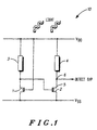
- An exemplary embodiment of the invention will now be described with reference to the single figure drawing which shows a preferred embodiment of a light detection device in accordance with the invention.
- Referring to the single figure drawing, there is shown a
light detection device 10, arranged to be integrated with an IC. - The
device 10 comprises a first transistor 1, having a gate terminal coupled to a supply voltage Vdd, a source terminal coupled to a ground terminal Vss and a drain terminal coupled to the supply voltage Vdd via a firsthigh impedance resistor 3. The first transistor 1 is thus arranged to provide a bias voltage to be further described below. - A
second transistor 2 of thedevice 10 has a gate terminal coupled to the drain terminal of the first transistor 1, a source terminal coupled to the ground terminal Vss and adrain terminal 5 coupled to the supply voltage Vdd via a second high impedance resistor 4, and further coupled to anoutput terminal 6. The high impedance resistor 4 is an undoped polysilicon resistor. - In operation, the gate terminal of the
second transistor 2 is arranged to receive the bias voltage from the drain terminal of the first transistor 1, the bias voltage being lower than the threshold voltage of the transistor. - When the
drain terminal 5 of the second transistor is subjected to incident visible light, a small reverse current is generated betweendrain 5 and the ground terminal Vss. This current flow lowers the voltage atdrain 5, and this voltage drop is detected by circuitry (not shown) coupled to theoutput terminal 6. - Since the second high impedance resistor is an undoped polysilicon resistor, extremely small currents can be detected, making the
device 10 very sensitive to incident light. - No parasitic reverse currents are generated, and during the manufacturing process of the
device 10, only one resistivity process is required to fabricate the first and the secondhigh impedance resistors 3 and 4, and this will not introduce variations which will significantly affect the performance of thedevice 10. - It will be appreciated that alternative embodiments to the one described above are possible. For example, the biasing arrangement may vary from the precise configuration described above. In addition, the first and second resistors could be fabricated from a material other than undoped polysilicon.
Claims (4)
- A light detection device (10) comprising:wherein incident visible light is detected by a voltage drop at the conducting electrode of the N channel transistor, characterized in that the resistor (4) is an undoped polysilicon resistor.a biasing circuit (1, 3) arranged to provide a bias voltage;a N channel transistor (2) having a control electrode arranged to receive the bias voltage which is lower than the threshold voltage of the transistor (2) and a conducting electrode (5); anda resistor (4) coupled between a supply voltage (VDD) and the conducting electrode of the transistor;
- The device of claim 1, wherein the biasing circuit comprises a biasing transistor (1) having a conducting electrode coupled to the supply voltage (VDD) via a biasing resistor (3).
- The device of claim 2 wherein the biasing resistor (3) is a high impedance resistor.
- The device of claim 3 wherein the biasing resistor (3) is an undoped polysilicon resistor.
Applications Claiming Priority (3)
| Application Number | Priority Date | Filing Date | Title |
|---|---|---|---|
| GB9624198A GB2319602B (en) | 1996-11-21 | 1996-11-21 | Light detection device |
| GB9624198 | 1996-11-21 | ||
| PCT/EP1997/006168 WO1998022905A1 (en) | 1996-11-21 | 1997-11-03 | Light detection device |
Publications (2)
| Publication Number | Publication Date |
|---|---|
| EP0939933A1 EP0939933A1 (en) | 1999-09-08 |
| EP0939933B1 true EP0939933B1 (en) | 2003-03-19 |
Family
ID=10803264
Family Applications (1)
| Application Number | Title | Priority Date | Filing Date |
|---|---|---|---|
| EP97948896A Expired - Lifetime EP0939933B1 (en) | 1996-11-21 | 1997-11-03 | Light detection device |
Country Status (7)
| Country | Link |
|---|---|
| US (1) | US6232591B1 (en) |
| EP (1) | EP0939933B1 (en) |
| JP (1) | JP2001504992A (en) |
| CN (1) | CN1146999C (en) |
| DE (1) | DE69720029T2 (en) |
| GB (1) | GB2319602B (en) |
| WO (1) | WO1998022905A1 (en) |
Families Citing this family (8)
| Publication number | Priority date | Publication date | Assignee | Title |
|---|---|---|---|---|
| KR100308216B1 (en) * | 1999-03-15 | 2001-09-26 | 윤종용 | Unauthorized unsealing detection apparatus for sealed electronic device |
| TW502286B (en) | 1999-12-09 | 2002-09-11 | Koninkl Philips Electronics Nv | Semiconductor device comprising a security coating and smartcard provided with such a device |
| DE10101995A1 (en) * | 2001-01-18 | 2002-07-25 | Philips Corp Intellectual Pty | Electrical or electronic switching arrangement comprises a detector unit and a comparator unit connected to the detector unit to compare the starting voltage with a reference voltage |
| DE10164419A1 (en) * | 2001-12-29 | 2003-07-17 | Philips Intellectual Property | Method and arrangement for protecting digital circuit parts |
| CN100347858C (en) * | 2002-10-31 | 2007-11-07 | 上海华虹集成电路有限责任公司 | Photo detection circuit |
| JP4613562B2 (en) * | 2004-09-27 | 2011-01-19 | ソニー株式会社 | Active matrix liquid crystal display device |
| CN114188363B (en) * | 2021-11-25 | 2025-07-25 | 京东方科技集团股份有限公司 | A flat panel detector, a driving method and a device thereof |
| CN121053920A (en) * | 2024-05-31 | 2025-12-02 | 京东方科技集团股份有限公司 | Display modules and display devices |
Family Cites Families (6)
| Publication number | Priority date | Publication date | Assignee | Title |
|---|---|---|---|---|
| JPS56150871A (en) * | 1980-04-24 | 1981-11-21 | Toshiba Corp | Semiconductor device |
| JPS6184054A (en) * | 1984-09-27 | 1986-04-28 | シーメンス、アクチエンゲゼルシヤフト | Intgrated mos circuit |
| JPS6290967A (en) * | 1985-10-17 | 1987-04-25 | Nissan Motor Co Ltd | Photodetecting semiconductor integrated circuit |
| FR2619959B1 (en) * | 1987-08-31 | 1991-06-14 | Thomson Semiconducteurs | LIGHT DETECTION CIRCUIT |
| JPH03101364A (en) * | 1989-09-13 | 1991-04-26 | Ricoh Co Ltd | Photoelectric converter |
| US5172211A (en) * | 1990-01-12 | 1992-12-15 | Paradigm Technology, Inc. | High resistance polysilicon load resistor |
-
1996
- 1996-11-21 GB GB9624198A patent/GB2319602B/en not_active Expired - Fee Related
-
1997
- 1997-11-03 WO PCT/EP1997/006168 patent/WO1998022905A1/en not_active Ceased
- 1997-11-03 JP JP52314998A patent/JP2001504992A/en not_active Ceased
- 1997-11-03 CN CNB971809569A patent/CN1146999C/en not_active Expired - Fee Related
- 1997-11-03 DE DE69720029T patent/DE69720029T2/en not_active Expired - Fee Related
- 1997-11-03 US US09/308,606 patent/US6232591B1/en not_active Expired - Lifetime
- 1997-11-03 EP EP97948896A patent/EP0939933B1/en not_active Expired - Lifetime
Also Published As
| Publication number | Publication date |
|---|---|
| WO1998022905A1 (en) | 1998-05-28 |
| JP2001504992A (en) | 2001-04-10 |
| GB2319602B (en) | 2000-10-04 |
| GB2319602A (en) | 1998-05-27 |
| CN1146999C (en) | 2004-04-21 |
| GB9624198D0 (en) | 1997-01-08 |
| US6232591B1 (en) | 2001-05-15 |
| CN1242093A (en) | 2000-01-19 |
| EP0939933A1 (en) | 1999-09-08 |
| DE69720029T2 (en) | 2003-11-27 |
| HK1024323A1 (en) | 2000-10-05 |
| DE69720029D1 (en) | 2003-04-24 |
Similar Documents
| Publication | Publication Date | Title |
|---|---|---|
| US5508548A (en) | General protection of an integrated circuit against permanent overloads and electrostatic discharges | |
| US8564364B2 (en) | Countermeasure method and device for protecting against a fault injection attack by detection of a well voltage crossing a threshold | |
| CN100433335C (en) | Electrically programmable antifuse and circuit formed therefrom | |
| US6016002A (en) | Stacked silicon-controlled rectifier having a low voltage trigger and adjustable holding voltage for ESD protection | |
| US4484244A (en) | Protection circuit for integrated circuit devices | |
| US6404269B1 (en) | Low power SOI ESD buffer driver networks having dynamic threshold MOSFETS | |
| US6844595B2 (en) | Electrostatic discharge protection circuit with high triggering voltage | |
| EP0343977A2 (en) | Mosfet having drain voltage detection function | |
| US6239958B1 (en) | Electrostatic damage protection circuit and dynamic random access memory | |
| JPH0729972A (en) | Semiconductor device | |
| US4952796A (en) | Light detection circuit having a junction reverse-biased by a current generator | |
| JPH06508958A (en) | monolithic integrated circuit device | |
| US6232591B1 (en) | Light detection device | |
| US6040733A (en) | Two-stage fusible electrostatic discharge protection circuit | |
| US4851894A (en) | Device for neutralizing the access to an integrated-circuit zone to be protected | |
| US5641981A (en) | Semiconductor apparatus and horizontal register for solid-state image pickup apparatus with protection circuit for bypassing an excess signal | |
| US6429491B1 (en) | Electrostatic discharge protection for MOSFETs | |
| US20030043517A1 (en) | Electro-static discharge protecting circuit | |
| EP0802604B1 (en) | Protection circuit | |
| EP0157389B1 (en) | Protection device for a mos transistor | |
| US7511355B2 (en) | Semiconductor device having fuse element | |
| US5969403A (en) | Physical fuse for semiconductor integrated circuit | |
| US4864454A (en) | Means for reducing damage to JFETs from electrostatic discharge events | |
| EP0218710A1 (en) | Cmos circuit. | |
| EP0211622B1 (en) | Mos integrated circuit having a protection circuit which includes divided protection resistors |
Legal Events
| Date | Code | Title | Description |
|---|---|---|---|
| PUAI | Public reference made under article 153(3) epc to a published international application that has entered the european phase |
Free format text: ORIGINAL CODE: 0009012 |
|
| 17P | Request for examination filed |
Effective date: 19990621 |
|
| AK | Designated contracting states |
Kind code of ref document: A1 Designated state(s): DE FR IT |
|
| RAP1 | Party data changed (applicant data changed or rights of an application transferred) |
Owner name: ATMEL RESEARCH |
|
| 17Q | First examination report despatched |
Effective date: 20010125 |
|
| GRAG | Despatch of communication of intention to grant |
Free format text: ORIGINAL CODE: EPIDOS AGRA |
|
| GRAG | Despatch of communication of intention to grant |
Free format text: ORIGINAL CODE: EPIDOS AGRA |
|
| GRAH | Despatch of communication of intention to grant a patent |
Free format text: ORIGINAL CODE: EPIDOS IGRA |
|
| GRAH | Despatch of communication of intention to grant a patent |
Free format text: ORIGINAL CODE: EPIDOS IGRA |
|
| GRAA | (expected) grant |
Free format text: ORIGINAL CODE: 0009210 |
|
| AK | Designated contracting states |
Designated state(s): DE FR IT |
|
| REF | Corresponds to: |
Ref document number: 69720029 Country of ref document: DE Date of ref document: 20030424 Kind code of ref document: P |
|
| ET | Fr: translation filed | ||
| PLBE | No opposition filed within time limit |
Free format text: ORIGINAL CODE: 0009261 |
|
| STAA | Information on the status of an ep patent application or granted ep patent |
Free format text: STATUS: NO OPPOSITION FILED WITHIN TIME LIMIT |
|
| 26N | No opposition filed |
Effective date: 20031222 |
|
| PGFP | Annual fee paid to national office [announced via postgrant information from national office to epo] |
Ref country code: DE Payment date: 20041129 Year of fee payment: 8 |
|
| PG25 | Lapsed in a contracting state [announced via postgrant information from national office to epo] |
Ref country code: IT Free format text: LAPSE BECAUSE OF NON-PAYMENT OF DUE FEES Effective date: 20051103 |
|
| PG25 | Lapsed in a contracting state [announced via postgrant information from national office to epo] |
Ref country code: DE Free format text: LAPSE BECAUSE OF NON-PAYMENT OF DUE FEES Effective date: 20060601 |
|
| REG | Reference to a national code |
Ref country code: FR Ref legal event code: TP |
|
| PGFP | Annual fee paid to national office [announced via postgrant information from national office to epo] |
Ref country code: FR Payment date: 20121206 Year of fee payment: 16 |
|
| REG | Reference to a national code |
Ref country code: FR Ref legal event code: ST Effective date: 20140731 |
|
| PG25 | Lapsed in a contracting state [announced via postgrant information from national office to epo] |
Ref country code: FR Free format text: LAPSE BECAUSE OF NON-PAYMENT OF DUE FEES Effective date: 20131202 |