EP0938211B1 - Flow control process using an out-of-band flow control channel - Google Patents
Flow control process using an out-of-band flow control channel Download PDFInfo
- Publication number
- EP0938211B1 EP0938211B1 EP98480072A EP98480072A EP0938211B1 EP 0938211 B1 EP0938211 B1 EP 0938211B1 EP 98480072 A EP98480072 A EP 98480072A EP 98480072 A EP98480072 A EP 98480072A EP 0938211 B1 EP0938211 B1 EP 0938211B1
- Authority
- EP
- European Patent Office
- Prior art keywords
- flow control
- cell
- process according
- empty
- information
- Prior art date
- Legal status (The legal status is an assumption and is not a legal conclusion. Google has not performed a legal analysis and makes no representation as to the accuracy of the status listed.)
- Expired - Lifetime
Links
- 238000000034 method Methods 0.000 title claims description 20
- 230000008569 process Effects 0.000 title claims description 18
- 230000022131 cell cycle Effects 0.000 claims description 7
- 238000004891 communication Methods 0.000 claims description 6
- 238000012544 monitoring process Methods 0.000 claims description 2
- 230000004044 response Effects 0.000 claims description 2
- 230000032258 transport Effects 0.000 description 11
- 230000005540 biological transmission Effects 0.000 description 7
- 230000008859 change Effects 0.000 description 6
- 230000007246 mechanism Effects 0.000 description 6
- 230000003068 static effect Effects 0.000 description 6
- 238000012545 processing Methods 0.000 description 5
- 101000687727 Homo sapiens Transcriptional regulator PINT87aa Proteins 0.000 description 2
- 102100024797 Transcriptional regulator PINT87aa Human genes 0.000 description 2
- 230000009467 reduction Effects 0.000 description 2
- 239000000872 buffer Substances 0.000 description 1
- 238000013461 design Methods 0.000 description 1
- 238000001514 detection method Methods 0.000 description 1
- 238000001914 filtration Methods 0.000 description 1
- 238000012423 maintenance Methods 0.000 description 1
- 230000003287 optical effect Effects 0.000 description 1
- 238000011084 recovery Methods 0.000 description 1
- 238000012827 research and development Methods 0.000 description 1
- 238000012546 transfer Methods 0.000 description 1
- 239000002699 waste material Substances 0.000 description 1
Images

Classifications
-
- H—ELECTRICITY
- H04—ELECTRIC COMMUNICATION TECHNIQUE
- H04L—TRANSMISSION OF DIGITAL INFORMATION, e.g. TELEGRAPHIC COMMUNICATION
- H04L47/00—Traffic control in data switching networks
- H04L47/10—Flow control; Congestion control
-
- H—ELECTRICITY
- H04—ELECTRIC COMMUNICATION TECHNIQUE
- H04L—TRANSMISSION OF DIGITAL INFORMATION, e.g. TELEGRAPHIC COMMUNICATION
- H04L12/00—Data switching networks
- H04L12/54—Store-and-forward switching systems
- H04L12/56—Packet switching systems
- H04L12/5601—Transfer mode dependent, e.g. ATM
- H04L12/5602—Bandwidth control in ATM Networks, e.g. leaky bucket
-
- H—ELECTRICITY
- H04—ELECTRIC COMMUNICATION TECHNIQUE
- H04L—TRANSMISSION OF DIGITAL INFORMATION, e.g. TELEGRAPHIC COMMUNICATION
- H04L47/00—Traffic control in data switching networks
- H04L47/10—Flow control; Congestion control
- H04L47/26—Flow control; Congestion control using explicit feedback to the source, e.g. choke packets
- H04L47/263—Rate modification at the source after receiving feedback
-
- H—ELECTRICITY
- H04—ELECTRIC COMMUNICATION TECHNIQUE
- H04L—TRANSMISSION OF DIGITAL INFORMATION, e.g. TELEGRAPHIC COMMUNICATION
- H04L49/00—Packet switching elements
- H04L49/25—Routing or path finding in a switch fabric
- H04L49/253—Routing or path finding in a switch fabric using establishment or release of connections between ports
- H04L49/255—Control mechanisms for ATM switching fabrics
-
- H—ELECTRICITY
- H04—ELECTRIC COMMUNICATION TECHNIQUE
- H04L—TRANSMISSION OF DIGITAL INFORMATION, e.g. TELEGRAPHIC COMMUNICATION
- H04L49/00—Packet switching elements
- H04L49/30—Peripheral units, e.g. input or output ports
- H04L49/3081—ATM peripheral units, e.g. policing, insertion or extraction
-
- H—ELECTRICITY
- H04—ELECTRIC COMMUNICATION TECHNIQUE
- H04L—TRANSMISSION OF DIGITAL INFORMATION, e.g. TELEGRAPHIC COMMUNICATION
- H04L12/00—Data switching networks
- H04L12/54—Store-and-forward switching systems
- H04L12/56—Packet switching systems
- H04L12/5601—Transfer mode dependent, e.g. ATM
- H04L2012/5614—User Network Interface
- H04L2012/5615—Network termination, e.g. NT1, NT2, PBX
-
- H—ELECTRICITY
- H04—ELECTRIC COMMUNICATION TECHNIQUE
- H04L—TRANSMISSION OF DIGITAL INFORMATION, e.g. TELEGRAPHIC COMMUNICATION
- H04L12/00—Data switching networks
- H04L12/54—Store-and-forward switching systems
- H04L12/56—Packet switching systems
- H04L12/5601—Transfer mode dependent, e.g. ATM
- H04L2012/5629—Admission control
- H04L2012/563—Signalling, e.g. protocols, reference model
-
- H—ELECTRICITY
- H04—ELECTRIC COMMUNICATION TECHNIQUE
- H04L—TRANSMISSION OF DIGITAL INFORMATION, e.g. TELEGRAPHIC COMMUNICATION
- H04L12/00—Data switching networks
- H04L12/54—Store-and-forward switching systems
- H04L12/56—Packet switching systems
- H04L12/5601—Transfer mode dependent, e.g. ATM
- H04L2012/5629—Admission control
- H04L2012/5631—Resource management and allocation
- H04L2012/5632—Bandwidth allocation
- H04L2012/5635—Backpressure, e.g. for ABR
-
- H—ELECTRICITY
- H04—ELECTRIC COMMUNICATION TECHNIQUE
- H04L—TRANSMISSION OF DIGITAL INFORMATION, e.g. TELEGRAPHIC COMMUNICATION
- H04L49/00—Packet switching elements
- H04L49/25—Routing or path finding in a switch fabric
-
- H—ELECTRICITY
- H04—ELECTRIC COMMUNICATION TECHNIQUE
- H04L—TRANSMISSION OF DIGITAL INFORMATION, e.g. TELEGRAPHIC COMMUNICATION
- H04L49/00—Packet switching elements
- H04L49/30—Peripheral units, e.g. input or output ports
Definitions
- the invention can be used in the telecommunication field and particularly in switching architectures which use serial telecommunication links transporting 8B/10B coding.
- Patent applications 96480126.0 (IBM Docket FR996040), 96480125.2 (IBM Docket FR996041), 96480117.9 (IBM Docket FR996042), 96480120.3 (IBM docket FR996045) are non published European applications illustrating a powerful self routing switch that provide high switch rate.
- Modem switching architectures requires powerful switching structures and distributed elements that provides with the attachment of the telecommunications lines.
- Such an architecture can be found the cop ending application filed at the priority date of the present application, and entitled " Flow control process for a switching system, and system for performing the same.”, and assigned to the assignee of the presents application, which is herein incorporated by simple reference.
- the central switching structure has some limited switching capacity it may obviously happen that, on one or more in ports, the switching structures requires to reduce the incoming flow of data that arrives in the port. Obviously this is achieved by means of a special channel that provides with the flow control information for that purpose.
- the problem to be solved by the present invention is to provide with a improved flow control channel for high speed switching architectures based on a centralized switching structure and distributed Switch Core Access Layers (S.C.A.L) entities that does not require additional physical media or use a minimum part of the available bandwith.
- S.C.A.L distributed Switch Core Access Layers
- the flow control channel of the present invention which uses two among the three available "comma characters" in order to create this specific flow control channel.
- the nature of the comma character that appears at the beginning of the cell provides with the appropriate flow control bit information.
- the receiving entity (either the switching structure or a distributed SCAL element) shall decode the latter as a positive flow control information, corresponding for instance to a request to reduce the incoming data flow.
- the receiving entity shall decode as an information according to which no reduction in the data flow is requested.
- the invention uses a predetermined bit within the data cell, generally that immediately follows the beginning of the cell, in order to carry the flow control information.
- the invention uses a second channel which is also based on the empty cells and which is used for transporting quasi static information that does not require immediate transport. This provides with an effective combination of two distinctive control channels, a first cell frequency channel such as defined above (providing a one-bit flow control channel at -the cell rate) and a second quasi static control channel for control information that does not need immediate transport or for which real time requirements are less importance.
- the invention can be improved by using an additionally specific mechanism that monitors, at the transmitting point, the change of one control information which is to be transport through the quasi static control channel. From the instant of the change, the mechanism initiates a counting process that automatically launches, if necessary, the creation of an empty cell so that the change of the considered control information can be transmitted and reported to the other side of the serial link within a maximum specified delay (also called edge distortion).
- a maximum specified delay also called edge distortion
- the invention also provides with a switching system having an effective flow control mechanism.
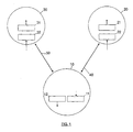
- FIG 1 With respect to figure 1 there is shown a switching structure 10 that is used for switching cells that come from different distributed Switch Core Access Layer entities.
- SCAL 20 that may be located within a first premise while a SCAL 30 can take place in another location.
- SCAL element is arranged in order to provide with the appropriate attachments to the particular telecommunication lines.
- a serial high speed communication link 40 is established between centralized switching structure 10 and SCAL 20 and a similar communication link 50 is established between structure 10 and SCAL 30.
- the communication links 40 and 50 between the centralized -switching structure and the corresponding SCAL entity is based on one or more individual serial electrical or optical link that transport cells with a 8B/10B appropriate encoding, such as described in prior art document "A DC-Balanced , partitionned-Block, 8B/10B Transmission Code " by A. X. Widmer et al, in IBM J. Res. Develop. , vol. 27, n 5, September 1983 and used as described "Single-chipx - Mbd CMOS Transceiver" in IEEE Journal of Solid-State Circuits, December 1996, Vol.31, number 12 by A.X. Widmer et al.
- a first control information is likely to change at the cell frequency, and is related to the most essential part of the switching mechanism, that is to say the flow control processing.
- Such an information which size appears to be very limited (even one bit per cell), must be transported at the cell rate in order to avoid any loss of information (in the case where the switching buffers be overloaded).
- this very limited information can be immediately transmitted by means of a specifically designed cell frequency channel. This is achieved by means of the use of two different comma characters among the three available ones in order to build this specific flow control channel.
- the receiving entity When the cells are idle or empty, the nature of the comma character that appears at the beginning of the cell provides with the appropriate flow control bit information. For instance, should the K.28.5 character be detected, the receiving entity (either the switching structure or a distributed SCAL element) shall decode the latter as a positive flow control information, corresponding for instance to a request to reduce the incoming data flow. Also, should the K.28.1 character be decoded, then the receiving entity shall decode it as an information according to which no reduction in the data flow is requested.
- the invention advantageously uses a predetermined bit within the data cell, generally one that is in the first byte of the data cell in order to carry the flow control information.
- the invention transports a second kind of control information that will be conveyed through a quasi static channel as hereinafter described.
- Such information include information that relates to maintenance and error recovery procedures and only requires a transport to the opposite side within a predetermined delay that correspond to a given edge distortion.
- this second kind of information is processed as follows.
- the invention uses a set of registers for storing the states of the control information to be conveyed.
- Switching structure 10 includes registers 11 and 12 .
- Register 11 stores the control bit information that is received from an internal (not shown) processor or specific hardware circuits and which to be transmitted through one of the two illustrated serial link.
- register 12 receives the control bit information from one of the two serial link, and provides with the latter to the internal processing unit or to the above mentioned hardware circuitry.
- SCAL 20 (resp. 30) includes two registers 21 and 22 (resp. 31 and 32).
- Register 21 (resp. register 31) stores the information that is received from serial link 40 (resp. 50) and which is to be provided to the internal electronic circuitry of SCAL 20 (resp. SCAL 30).
- Register 22 (resp. register 32) stores the information that is received from the internal hardware circuit inside SCAL 20 (resp. SCAL 30) and which has to be conveyed through the serial link 40 (resp. 50).
- register 11 In order to ensure optimal operating of the switch, it is absolutely necessary that the contents of register 11 must be reported and copied within register 21 (resp. 31) during the specified delay that complies with the desired edge distortion specifications. Conversely, the contents of the register 22 (resp. 32) must be conveyed through the corresponding link and reported to register 12 of switching structure 10. In the preferred embodiment of the invention, this is achieved by means of a second quasi static channel which is based on the empty cells. Considering for instance the transport of the control information that is stored within register 11 and which must be conveyed through link 40, and copied into register 22.
- the cell transmission system that is used within switching structure uses the contents of register 11 and transmits the latter at a predetermined position within the empty cell that begins with a comma character.
- comma character is one of the two comma characters mentioned above so that, concurrently, the two types of control information - the flow control and the control information - can be transported.
- the contents of register 11 is located in the first byte that immediately follows the comma character. This information can then be detected and reported into the corresponding register 21 (resp. 31 ) of SCAL 20 (resp. SCAL 30).
- the man skilled in the art will obviously design the circuit achieves the comma character -detection, and then provides with the transfer of the contents of a predetermined position of the cell into the appropriate register 21 (resp. 31).
- register 22 (resp. 32) is transmitted in empty cells at a predetermined location, which is, in the preferred embodiment, the first byte of the empty cell so that the contents can be copied into register 12 of centralized switching structure 10.
- the quasi static channel in accordance with the present invention is enhanced by an additional mechanism that ensures that the contents of the registers 11 (within centralized structure 10 ) be reported into its corresponding register 21 (resp. 31) within an maximum delay that corresponds to the desired edge distortion requirements.
- a monitoring circuit is used for detecting any change within the contents of register 11 and, in response to such a change, to initiates a counting process of k cell cycles.
- the mechanism uses that empty cell in order to transport the contents of register 11 and reset the counting process.
- the invention launches the creation of an empty cell that will ensure the transportation of the contents of register 11 to the corresponding register 21 (resp. 31) at the opposition side of SCAL 20 (resp. SCAL 30). Therefore, the maximal distortion will be limited to k cell cycles.
- the creation of the empty cell is advantageously performed by means the creation of a local flow control signal such as illustrated in figures 2 and 3.
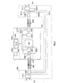
- Figures 2 and 3 show the particular structure of the centralized switching structure 10, and the SCAL entity 20 (resp. 30) and which is particularly described in the above mentioned cop ending application.
- FIG 2 there is shown how the local flow control signal is generated in order to create an empty cell so that the contents of register 11 can be transported through the serial link 40 (resp. 50).
- the centralized switching structure 1130 comprises a switch core element 450 providing with the switching of a set of n input and output ports, a set of n dedicated modules 1110, one module for one input and output port, that comprises a deserializer DES 1170, a serializer SER 1190, a set of two routing control circuits 1001-i and 1010-i whose function is described with many details in the above mentioned application, and a cell storage 1 which is used for providing some queuing resources for the data cells.
- the centralized switching structure 1130 further comprises processing resources under the form of a processor 1160 and a set of n storage 1120 that provides the space required for the storage of the routing bit map that is associated to the routing index.
- module 1110 uses a edge detector for detecting the changes brought to register 11 (not shown in the figure 2) and a hardware counter that is used for counter a predetermined number of cell cycles (for instance k).
- a hardware counter that is used for counter a predetermined number of cell cycles (for instance k).
- FCX flow control Transmit signal causes an empty cycle at the output port of 450 and, thus, provides serializer 1190 with an appropriate empty cell that is used for transport the state of the register 11.
- module 1115 uses a edge detector for detecting the changes brought to register 22 (not shown in the figure 3) and a hardware counter that is used for counter a predetermined number of cell cycles (for instance k).
- the SER serializer 1160 that is represented in the figure 3 transmits an empty cell through the serial link, the latter incorporates the contents of the register 22 into the cell, at the appropriate location so that it can be detected by the deserializer 1170 at the opposite side of the serial link 40 (represented by multiwires 1400) and finally copied into the register 12 (not shown in Figure 3).
Landscapes
- Engineering & Computer Science (AREA)
- Computer Networks & Wireless Communication (AREA)
- Signal Processing (AREA)
- Data Exchanges In Wide-Area Networks (AREA)
Description
- The invention can be used in the telecommunication field and particularly in switching architectures which use serial telecommunication links transporting 8B/10B coding.
- Patent applications 96480126.0 (IBM Docket FR996040), 96480125.2 (IBM Docket FR996041), 96480117.9 (IBM Docket FR996042), 96480120.3 (IBM docket FR996045) are non published European applications illustrating a powerful self routing switch that provide high switch rate.
- Modem switching architectures requires powerful switching structures and distributed elements that provides with the attachment of the telecommunications lines. Such an architecture can be found the cop ending application filed at the priority date of the present application, and entitled " Flow control process for a switching system, and system for performing the same.", and assigned to the assignee of the presents application, which is herein incorporated by simple reference.
- Since the central switching structure has some limited switching capacity it may obviously happen that, on one or more in ports, the switching structures requires to reduce the incoming flow of data that arrives in the port. Obviously this is achieved by means of a special channel that provides with the flow control information for that purpose.
- However since the distance between the switching structure and the different distributed entities (SCAL elements) that can be located in different premises within an industrial area tends to increase, even attaining some hundreds of meters, it is highly desirable that flow control channel does not use some additional physical media. Known techniques to provide such flow control channels may use cell overhead by dedicating some of the bits that are -conveyed to this particular flow control information. However, this results in the waste of the useful bandwith.
- This requirement is even more critical when the switching architecture is based on a port expansion mode, resulting in a great number of individual switches being connected.
- International Patent Application WO 95 30318 (Bews Steve et al.; Newbridge Networks Corp (CA)) entitled "ATM Switching System" discloses a communication system comprising a hub slot adapted to receive any one of a plurality of hub cards for receiving and transmitting data cells; a plurality of universal card slots; a plurality of interface cards insertable into any one of said plurality of universal card slots for receiving incoming ones of said data cells containing data and transmitting outgoing ones of said data cells containing data; an add bus having respective data links connected between individual ones of said universal card slots and said hub slot for receiving said outgoing ones of said data cells from said plurality of interface cards and transmitting said outgoing ones of said data cells to said hub slot; a drop bus having a single data link connected between all of said universal card slots and said hub slot for transmitting said incoming ones of said data cells from said hub slot to said plurality of interface cards; and means within each of said interface cards for filtering said incoming ones of said data cells from said drop bus and thereby routing said data cells to an appropriate one or more of said plurality of interface cards.
- Article in IBM Journal of Research and Development entitled "A DC-Balanced, Partitioned-Block, 8B/10B Transmission Code" (Widmer A X et al.), vol.27, no.5, 1 September 1983, pages 440-451, discloses a byte-oriented binary transmission code and its implementation. This code is directed to high-speed local area networks and similar data links, where the information format consists of packets, variable in length, from about a dozen up to several hundred 8-bit bytes. The proposed transmission code translates each source byte into a constrained 10-bit binary sequence which has performance parameters near the theoretical limits for 8B/10B codes. The maximum run length is 5 and the maximum digital sum variation is 6. A single error in the encoded bits can, at most, generate an error burst of length 5 in the decoded domain. The code is implemented by partioning the coder into 5B/6B and 3B/4B subordinate coders.
- The problem to be solved by the present invention is to provide with a improved flow control channel for high speed switching architectures based on a centralized switching structure and distributed Switch Core Access Layers (S.C.A.L) entities that does not require additional physical media or use a minimum part of the available bandwith.
- It is an object of the present invention to provide with a flow control channel for a switching architecture which can be used even when it is mounted on a port expansion.
- This problem is solved by the flow control channel of the present invention which uses two among the three available "comma characters" in order to create this specific flow control channel. When the cells are idle or empty, the nature of the comma character that appears at the beginning of the cell provides with the appropriate flow control bit information. For instance, should the K.28.5 character be detected, the receiving entity (either the switching structure or a distributed SCAL element) shall decode the latter as a positive flow control information, corresponding for instance to a request to reduce the incoming data flow. Also, should the K.28.1 character be decoded, then the receiving entity shall decode as an information according to which no reduction in the data flow is requested. When the incoming flow provides with data cells, the invention uses a predetermined bit within the data cell, generally that immediately follows the beginning of the cell, in order to carry the flow control information. Preferably, the invention uses a second channel which is also based on the empty cells and which is used for transporting quasi static information that does not require immediate transport. This provides with an effective combination of two distinctive control channels, a first cell frequency channel such as defined above (providing a one-bit flow control channel at -the cell rate) and a second quasi static control channel for control information that does not need immediate transport or for which real time requirements are less importance.
- Thirdly, the invention can be improved by using an additionally specific mechanism that monitors, at the transmitting point, the change of one control information which is to be transport through the quasi static control channel. From the instant of the change, the mechanism initiates a counting process that automatically launches, if necessary, the creation of an empty cell so that the change of the considered control information can be transmitted and reported to the other side of the serial link within a maximum specified delay (also called edge distortion).
- The invention also provides with a switching system having an effective flow control mechanism.
-
- Figure 1 illustrates a switching architecture based on a centralized switching structure and some distributed SCAL entities.
- Figures 2 and 3 illustrate a preferred embodiment of the invention.
-
- With respect to figure 1 there is shown a
switching structure 10 that is used for switching cells that come from different distributed Switch Core Access Layer entities. For clarity's purpose two distinctive SCAL entities are represented on the figure: SCAL 20 that may be located within a first premise while a SCAL 30 can take place in another location. Each SCAL element is arranged in order to provide with the appropriate attachments to the particular telecommunication lines. - A serial high
speed communication link 40 is established between centralizedswitching structure 10 and SCAL 20 and asimilar communication link 50 is established betweenstructure 10 and SCAL 30. The communication links 40 and 50 between the centralized -switching structure and the corresponding SCAL entity is based on one or more individual serial electrical or optical link that transport cells with a 8B/10B appropriate encoding, such as described in prior art document "A DC-Balanced , partitionned-Block, 8B/10B Transmission Code " by A. X. Widmer et al, in IBM J. Res. Develop. , vol. 27, n 5, September 1983 and used as described "Single-chipx - Mbd CMOS Transceiver" in IEEE Journal of Solid-State Circuits, December 1996, Vol.31,number 12 by A.X. Widmer et al. - However, it is necessary to be able to transport some control information between the switching structure and the SCAL. Two different control information coexist. A first control information is likely to change at the cell frequency, and is related to the most essential part of the switching mechanism, that is to say the flow control processing. Such an information, which size appears to be very limited (even one bit per cell), must be transported at the cell rate in order to avoid any loss of information (in the case where the switching buffers be overloaded). In the invention, this very limited information can be immediately transmitted by means of a specifically designed cell frequency channel. This is achieved by means of the use of two different comma characters among the three available ones in order to build this specific flow control channel. When the cells are idle or empty, the nature of the comma character that appears at the beginning of the cell provides with the appropriate flow control bit information. For instance, should the K.28.5 character be detected, the receiving entity (either the switching structure or a distributed SCAL element) shall decode the latter as a positive flow control information, corresponding for instance to a request to reduce the incoming data flow. Also, should the K.28.1 character be decoded, then the receiving entity shall decode it as an information according to which no reduction in the data flow is requested. When the incoming flow provides with data cells, no comma character appears in the data flow and, in this case, the invention advantageously uses a predetermined bit within the data cell, generally one that is in the first byte of the data cell in order to carry the flow control information.
- In addition to the flow control information that must be transported via the serial link at the cell rate, the invention transports a second kind of control information that will be conveyed through a quasi static channel as hereinafter described. Such information include information that relates to maintenance and error recovery procedures and only requires a transport to the opposite side within a predetermined delay that correspond to a given edge distortion. In the invention, this second kind of information is processed as follows. In the centralized switching structures, as well as the associated distributed SCAL elements, the invention uses a set of registers for storing the states of the control information to be conveyed. For instance,
Switching structure 10 includesregisters register 12 receives the control bit information from one of the two serial link, and provides with the latter to the internal processing unit or to the above mentioned hardware circuitry. Similarly, SCAL 20 (resp. 30) includes tworegisters 21 and 22 (resp. 31 and 32). Register 21 (resp. register 31) stores the information that is received from serial link 40 (resp. 50) and which is to be provided to the internal electronic circuitry of SCAL 20 (resp. SCAL 30). Register 22 (resp. register 32) stores the information that is received from the internal hardware circuit inside SCAL 20 (resp. SCAL 30) and which has to be conveyed through the serial link 40 (resp. 50). - In order to ensure optimal operating of the switch, it is absolutely necessary that the contents of
register 11 must be reported and copied within register 21 (resp. 31) during the specified delay that complies with the desired edge distortion specifications. Conversely, the contents of the register 22 (resp. 32) must be conveyed through the corresponding link and reported to register 12 of switchingstructure 10. In the preferred embodiment of the invention, this is achieved by means of a second quasi static channel which is based on the empty cells. Considering for instance the transport of the control information that is stored withinregister 11 and which must be conveyed throughlink 40, and copied intoregister 22. - When no data cell is to be transmitted, the cell transmission system that is used within switching structure uses the contents of
register 11 and transmits the latter at a predetermined position within the empty cell that begins with a comma character. It should be noticed that comma character is one of the two comma characters mentioned above so that, concurrently, the two types of control information - the flow control and the control information - can be transported. In the preferred embodiment of the invention, the contents ofregister 11 is located in the first byte that immediately follows the comma character. This information can then be detected and reported into the corresponding register 21 (resp. 31 ) of SCAL 20 (resp. SCAL 30). The man skilled in the art will obviously design the circuit achieves the comma character -detection, and then provides with the transfer of the contents of a predetermined position of the cell into the appropriate register 21 (resp. 31). - Similarly, the contents of register 22 (resp. 32) is transmitted in empty cells at a predetermined location, which is, in the preferred embodiment, the first byte of the empty cell so that the contents can be copied into
register 12 ofcentralized switching structure 10. - The quasi static channel in accordance with the present invention is enhanced by an additional mechanism that ensures that the contents of the registers 11 (within centralized structure 10 ) be reported into its corresponding register 21 (resp. 31) within an maximum delay that corresponds to the desired edge distortion requirements. To achieve this, a monitoring circuit is used for detecting any change within the contents of
register 11 and, in response to such a change, to initiates a counting process of k cell cycles. When an empty cell appears to be transmitted by centralized structure 10 - because of a instantaneous lack of data cell, the mechanism uses that empty cell in order to transport the contents ofregister 11 and reset the counting process. However, when the counting process completes without the occurrence of any empty cell, the invention launches the creation of an empty cell that will ensure the transportation of the contents ofregister 11 to the corresponding register 21 (resp. 31) at the opposition side of SCAL 20 (resp. SCAL 30). Therefore, the maximal distortion will be limited to k cell cycles. - In the invention, the creation of the empty cell is advantageously performed by means the creation of a local flow control signal such as illustrated in figures 2 and 3. Figures 2 and 3 show the particular structure of the
centralized switching structure 10, and the SCAL entity 20 (resp. 30) and which is particularly described in the above mentioned cop ending application. - In figure 2, there is shown how the local flow control signal is generated in order to create an empty cell so that the contents of
register 11 can be transported through the serial link 40 (resp. 50). - Basically, the
centralized switching structure 1130 comprises aswitch core element 450 providing with the switching of a set of n input and output ports, a set of n dedicatedmodules 1110, one module for one input and output port, that comprises adeserializer DES 1170, aserializer SER 1190, a set of two routing control circuits 1001-i and 1010-i whose function is described with many details in the above mentioned application, and acell storage 1 which is used for providing some queuing resources for the data cells. Thecentralized switching structure 1130 further comprises processing resources under the form of aprocessor 1160 and a set ofn storage 1120 that provides the space required for the storage of the routing bit map that is associated to the routing index. - In order to achieve the empty cell creation,
module 1110 uses a edge detector for detecting the changes brought to register 11 (not shown in the figure 2) and a hardware counter that is used for counter a predetermined number of cell cycles (for instance k). In the invention, whenever theSER serializer 1190 that is represented in the figure 2 transmits an empty cell through the serial link, the latter incorporates the contents of theregister 11 into the cell, at the appropriate location so that it can be detected by thedeserializer 1180 at the opposite side of the serial link 40 (represented by multiwires 4400) and finally copied into the register 21 (not shown in Figure 2). - When the counting process reaches the k value without occurrence of an empty cell, then a specific processing occurs within the boundaries of
module 1110, what causes deserializer 1170 to transmit a FCX flow control Transmit signal on lead 9500-i to theswitch core element 450 during one cell cycle. The transmission of this signal is particularly described in the above mentioned application, and is very simple to embody since themodule 1110 and theswitch core 450 are located at the same physical area. This FCX flow control transmit signal causes an empty cycle at the output port of 450 and, thus, providesserializer 1190 with an appropriate empty cell that is used for transport the state of theregister 11. - With respect to figure 3, there is shown the creation of an empty cell between
SCAL 20 and switchingstructure 10 so that the contents of register 22 (for instance) withinSCAL element 20 can be conveyed to switchingstructure 10. In order to achieve the empty cell creation,module 1115 uses a edge detector for detecting the changes brought to register 22 (not shown in the figure 3) and a hardware counter that is used for counter a predetermined number of cell cycles (for instance k). - In the invention, whenever the
SER serializer 1160 that is represented in the figure 3 transmits an empty cell through the serial link, the latter incorporates the contents of theregister 22 into the cell, at the appropriate location so that it can be detected by thedeserializer 1170 at the opposite side of the serial link 40 (represented by multiwires 1400) and finally copied into the register 12 (not shown in Figure 3). - When the counting process reaches the value k without occurrence of an empty cell, then a specific processing occurs within the boundaries of
module 1115, what causes deserializer 1180 to transmit a FCR flow control Receive signal on lead 9520-i to the PINT element 511-i during one cell cycle. The transmission of this signal is particularly described in the above mentioned application, and is very simple to embody since themodule 1115 and thePINT 511 are located at the same physical area. This FCR flow control receive signal causes an empty cycle at the output port of 511 and, thus, providesserializer 1160 with an appropriate empty cell that is used for the transport the state of theregister 22.
Claims (9)
- Process for controlling data flow of a switching architecture comprising a switching structure (10) and distributed Switch Core Access Layer elements (20, 30) connected through at least one communication links (40, 50) wherein the data flow is coded in accordance with the 8B/10B coding, characterized in that :two among three available Comma characters are inserted in empty cells and used for creating an additional flow control channel which is parallely conveyed with the normal data flow, wherein the nature of the Comma character that appears at the beginning of an idle or empty cell provides flow control information.
- The process according to claim 1 wherein, when the cell are idle or empty, the nature of the comma character appearing at the beginning of the cell provides with the appropriate flow control bit information to be transmitted on said communication link.
- The process according to claim 1 or 2 wherein a K.28.5 comma character is used and decoded by the receiving entity as a positive flow control information corresponding to a request to reduce the data flow.
- The process according to any one of claims 1 to 3 wherein when an incoming flow provides data cells, a predetermined bit is used within the data cells for carrying the flow control information.
- The process according to any one of claims 1 to 4, further comprising the step of using the empty cells as a second channel for transporting quasi-static information that does not require immediate transport.
- The process according to claim 5 wherein the quasi-static information is copied into the empty cell following the comma character for transport with the cell.
- The process according to claim 6 wherein the quasi-static information is to be transported within a maximum amount of time after a triggering event and wherein the process further comprises the steps of:monitoring for the trigering event;tracking the time passed following the trigering event;in response to the passage of the maximum time after the triggering event without transporting the quasi-static information, causing an empty cell to be transported through the switching structure.
- The process according to claim 7 wherein the triggering event is an updating of the quasi-static information and wherein the maximum time is counted in cell cycles.
- System comprising means adapted for carrying out the process according to any one of the preceding claims.
Priority Applications (1)
| Application Number | Priority Date | Filing Date | Title |
|---|---|---|---|
| EP98480072A EP0938211B1 (en) | 1998-02-19 | 1998-10-29 | Flow control process using an out-of-band flow control channel |
Applications Claiming Priority (3)
| Application Number | Priority Date | Filing Date | Title |
|---|---|---|---|
| EP98480006 | 1998-02-19 | ||
| EP98480006 | 1998-02-19 | ||
| EP98480072A EP0938211B1 (en) | 1998-02-19 | 1998-10-29 | Flow control process using an out-of-band flow control channel |
Publications (3)
| Publication Number | Publication Date |
|---|---|
| EP0938211A2 EP0938211A2 (en) | 1999-08-25 |
| EP0938211A3 EP0938211A3 (en) | 2001-01-10 |
| EP0938211B1 true EP0938211B1 (en) | 2003-10-22 |
Family
ID=26151814
Family Applications (1)
| Application Number | Title | Priority Date | Filing Date |
|---|---|---|---|
| EP98480072A Expired - Lifetime EP0938211B1 (en) | 1998-02-19 | 1998-10-29 | Flow control process using an out-of-band flow control channel |
Country Status (1)
| Country | Link |
|---|---|
| EP (1) | EP0938211B1 (en) |
Families Citing this family (1)
| Publication number | Priority date | Publication date | Assignee | Title |
|---|---|---|---|---|
| WO2011075492A1 (en) | 2009-12-18 | 2011-06-23 | Dow Global Technologies Llc | Films and articles prepared from the same |
Family Cites Families (3)
| Publication number | Priority date | Publication date | Assignee | Title |
|---|---|---|---|---|
| US4958341A (en) * | 1988-03-31 | 1990-09-18 | At&T Bell Laboratories | Integrated packetized voice and data switching system |
| GB9408574D0 (en) * | 1994-04-29 | 1994-06-22 | Newbridge Networks Corp | Atm switching system |
| US5638518A (en) * | 1994-10-24 | 1997-06-10 | Lsi Logic Corporation | Node loop core for implementing transmission protocol in fibre channel |
-
1998
- 1998-10-29 EP EP98480072A patent/EP0938211B1/en not_active Expired - Lifetime
Also Published As
| Publication number | Publication date |
|---|---|
| EP0938211A3 (en) | 2001-01-10 |
| EP0938211A2 (en) | 1999-08-25 |
Similar Documents
| Publication | Publication Date | Title |
|---|---|---|
| US6606300B1 (en) | Flow control process for a switching system and system for performing the same | |
| US5610745A (en) | Method and apparatus for tracking buffer availability | |
| EP1137225B1 (en) | A switch and a switching method | |
| US6092108A (en) | Dynamic threshold packet filtering of application processor frames | |
| US6798744B1 (en) | Method and apparatus for interconnection of flow-controlled communication | |
| CA2489973C (en) | Redundant communication network of the switched full-duplex ethernet type and a management method of the redundancy of such a network, notably in the avionic domain | |
| CA2270094C (en) | Parallel backplane physical layer interface with scalable data bandwidth | |
| US6343081B1 (en) | Method and apparatus for managing contention in a self-routing switching architecture in a port expansion mode | |
| US6934301B2 (en) | Method and apparatus for converting data packets between a higher bandwidth network and a lower bandwidth network | |
| US20060083185A1 (en) | Method and apparatus for generic interface, packet cut-through, overbooking, queue concatenation, and logical identification priority for a system packet interface device | |
| JPH0799830B2 (en) | Communication protocol for a statistical data multiplexer incorporated in a wide area network. | |
| JP2007517334A (en) | Buffer management via non-data code handling point-to-point links | |
| FI85319B (en) | The coupling element. | |
| US7415031B2 (en) | Data link/physical layer packet diversion and insertion | |
| US4160877A (en) | Multiplexing of bytes of non-uniform length with end of time slot indicator | |
| US7199732B1 (en) | Data converter with reduced component count for padded-protocol interface | |
| KR100339463B1 (en) | Parallel on-the-fly processing of fixed length cells | |
| US7088680B1 (en) | System and method for digital communication via a time division multiplexed serial data stream | |
| US6690670B1 (en) | System and method for transmission between ATM layer devices and PHY layer devices over a serial bus | |
| US6452900B1 (en) | Flow control process for a switching architecture using an out-of-band flow control channel and apparatus for performing the same | |
| US7411969B2 (en) | Method, system, and apparatus for a credit based flow control in a computer system | |
| US7688839B2 (en) | Data link/physical layer packet buffering and flushing | |
| EP0938211A2 (en) | Flow control process using an out-of-band flow control channel | |
| EP0976230A2 (en) | Device for and method of transmission of digital signals, in particular in dect-type systems | |
| CN111722940B (en) | Message transmission method, terminal equipment and transmission system based on asynchronous serial port |
Legal Events
| Date | Code | Title | Description |
|---|---|---|---|
| PUAI | Public reference made under article 153(3) epc to a published international application that has entered the european phase |
Free format text: ORIGINAL CODE: 0009012 |
|
| AK | Designated contracting states |
Kind code of ref document: A2 Designated state(s): DE FR GB |
|
| AX | Request for extension of the european patent |
Free format text: AL;LT;LV;MK;RO;SI |
|
| PUAL | Search report despatched |
Free format text: ORIGINAL CODE: 0009013 |
|
| AK | Designated contracting states |
Kind code of ref document: A3 Designated state(s): AT BE CH CY DE DK ES FI FR GB GR IE IT LI LU MC NL PT SE |
|
| AX | Request for extension of the european patent |
Free format text: AL;LT;LV;MK;RO;SI |
|
| 17P | Request for examination filed |
Effective date: 20010427 |
|
| AKX | Designation fees paid |
Free format text: DE FR GB |
|
| 17Q | First examination report despatched |
Effective date: 20020207 |
|
| GRAH | Despatch of communication of intention to grant a patent |
Free format text: ORIGINAL CODE: EPIDOS IGRA |
|
| GRAS | Grant fee paid |
Free format text: ORIGINAL CODE: EPIDOSNIGR3 |
|
| GRAA | (expected) grant |
Free format text: ORIGINAL CODE: 0009210 |
|
| AK | Designated contracting states |
Kind code of ref document: B1 Designated state(s): DE FR GB |
|
| REG | Reference to a national code |
Ref country code: GB Ref legal event code: FG4D |
|
| REF | Corresponds to: |
Ref document number: 69819129 Country of ref document: DE Date of ref document: 20031127 Kind code of ref document: P |
|
| ET | Fr: translation filed | ||
| PLBE | No opposition filed within time limit |
Free format text: ORIGINAL CODE: 0009261 |
|
| STAA | Information on the status of an ep patent application or granted ep patent |
Free format text: STATUS: NO OPPOSITION FILED WITHIN TIME LIMIT |
|
| 26N | No opposition filed |
Effective date: 20040723 |
|
| REG | Reference to a national code |
Ref country code: GB Ref legal event code: 746 Effective date: 20080925 |
|
| PGFP | Annual fee paid to national office [announced via postgrant information from national office to epo] |
Ref country code: FR Payment date: 20101018 Year of fee payment: 13 |
|
| REG | Reference to a national code |
Ref country code: FR Ref legal event code: ST Effective date: 20120629 |
|
| PG25 | Lapsed in a contracting state [announced via postgrant information from national office to epo] |
Ref country code: FR Free format text: LAPSE BECAUSE OF NON-PAYMENT OF DUE FEES Effective date: 20111102 |
|
| PGFP | Annual fee paid to national office [announced via postgrant information from national office to epo] |
Ref country code: DE Payment date: 20171024 Year of fee payment: 20 |
|
| PGFP | Annual fee paid to national office [announced via postgrant information from national office to epo] |
Ref country code: GB Payment date: 20171030 Year of fee payment: 20 |
|
| REG | Reference to a national code |
Ref country code: DE Ref legal event code: R071 Ref document number: 69819129 Country of ref document: DE |
|
| REG | Reference to a national code |
Ref country code: GB Ref legal event code: PE20 Expiry date: 20181028 |
|
| PG25 | Lapsed in a contracting state [announced via postgrant information from national office to epo] |
Ref country code: GB Free format text: LAPSE BECAUSE OF EXPIRATION OF PROTECTION Effective date: 20181028 |