EP0936452B1 - Method and apparatus for calibration of a multi-channel fiber optic interferometric sensor system in a signal processing system - Google Patents
Method and apparatus for calibration of a multi-channel fiber optic interferometric sensor system in a signal processing system Download PDFInfo
- Publication number
- EP0936452B1 EP0936452B1 EP99300974A EP99300974A EP0936452B1 EP 0936452 B1 EP0936452 B1 EP 0936452B1 EP 99300974 A EP99300974 A EP 99300974A EP 99300974 A EP99300974 A EP 99300974A EP 0936452 B1 EP0936452 B1 EP 0936452B1
- Authority
- EP
- European Patent Office
- Prior art keywords
- phase
- laser module
- phase modulation
- average
- component
- Prior art date
- Legal status (The legal status is an assumption and is not a legal conclusion. Google has not performed a legal analysis and makes no representation as to the accuracy of the status listed.)
- Expired - Lifetime
Links
- 238000000034 method Methods 0.000 title claims description 31
- 238000012545 processing Methods 0.000 title claims description 22
- 239000000835 fiber Substances 0.000 title description 21
- 230000003287 optical effect Effects 0.000 claims description 8
- 230000001419 dependent effect Effects 0.000 claims description 5
- 238000004836 empirical method Methods 0.000 claims 1
- 230000010363 phase shift Effects 0.000 description 11
- 238000003491 array Methods 0.000 description 10
- 238000010586 diagram Methods 0.000 description 7
- 230000008859 change Effects 0.000 description 4
- 239000013307 optical fiber Substances 0.000 description 4
- 230000010287 polarization Effects 0.000 description 4
- 230000008569 process Effects 0.000 description 4
- 239000000872 buffer Substances 0.000 description 3
- 239000013078 crystal Substances 0.000 description 3
- 230000008901 benefit Effects 0.000 description 2
- 238000004364 calculation method Methods 0.000 description 2
- 238000005562 fading Methods 0.000 description 2
- 238000001914 filtration Methods 0.000 description 2
- 238000012986 modification Methods 0.000 description 2
- 230000004048 modification Effects 0.000 description 2
- COCLLEMEIJQBAG-UHFFFAOYSA-N 8-methylnonyl 2-methylprop-2-enoate Chemical compound CC(C)CCCCCCCOC(=O)C(C)=C COCLLEMEIJQBAG-UHFFFAOYSA-N 0.000 description 1
- 101000798707 Homo sapiens Transmembrane protease serine 13 Proteins 0.000 description 1
- 230000018199 S phase Effects 0.000 description 1
- 102100032467 Transmembrane protease serine 13 Human genes 0.000 description 1
- 230000006978 adaptation Effects 0.000 description 1
- 239000000969 carrier Substances 0.000 description 1
- 239000003086 colorant Substances 0.000 description 1
- 239000002131 composite material Substances 0.000 description 1
- 230000003750 conditioning effect Effects 0.000 description 1
- 238000001514 detection method Methods 0.000 description 1
- 238000011161 development Methods 0.000 description 1
- 230000018109 developmental process Effects 0.000 description 1
- 229920005994 diacetyl cellulose Polymers 0.000 description 1
- 238000005553 drilling Methods 0.000 description 1
- 238000005516 engineering process Methods 0.000 description 1
- 230000006870 function Effects 0.000 description 1
- 230000010354 integration Effects 0.000 description 1
- GQYHUHYESMUTHG-UHFFFAOYSA-N lithium niobate Chemical compound [Li+].[O-][Nb](=O)=O GQYHUHYESMUTHG-UHFFFAOYSA-N 0.000 description 1
- 230000003278 mimic effect Effects 0.000 description 1
- 239000000203 mixture Substances 0.000 description 1
- 230000005405 multipole Effects 0.000 description 1
- 230000004044 response Effects 0.000 description 1
- 238000010187 selection method Methods 0.000 description 1
- 238000012360 testing method Methods 0.000 description 1
- 239000013598 vector Substances 0.000 description 1
- 238000012795 verification Methods 0.000 description 1
- 230000000007 visual effect Effects 0.000 description 1
- 239000013585 weight reducing agent Substances 0.000 description 1
Images



Classifications
-
- G—PHYSICS
- G01—MEASURING; TESTING
- G01D—MEASURING NOT SPECIALLY ADAPTED FOR A SPECIFIC VARIABLE; ARRANGEMENTS FOR MEASURING TWO OR MORE VARIABLES NOT COVERED IN A SINGLE OTHER SUBCLASS; TARIFF METERING APPARATUS; MEASURING OR TESTING NOT OTHERWISE PROVIDED FOR
- G01D5/00—Mechanical means for transferring the output of a sensing member; Means for converting the output of a sensing member to another variable where the form or nature of the sensing member does not constrain the means for converting; Transducers not specially adapted for a specific variable
- G01D5/26—Mechanical means for transferring the output of a sensing member; Means for converting the output of a sensing member to another variable where the form or nature of the sensing member does not constrain the means for converting; Transducers not specially adapted for a specific variable characterised by optical transfer means, i.e. using infrared, visible, or ultraviolet light
- G01D5/32—Mechanical means for transferring the output of a sensing member; Means for converting the output of a sensing member to another variable where the form or nature of the sensing member does not constrain the means for converting; Transducers not specially adapted for a specific variable characterised by optical transfer means, i.e. using infrared, visible, or ultraviolet light with attenuation or whole or partial obturation of beams of light
- G01D5/34—Mechanical means for transferring the output of a sensing member; Means for converting the output of a sensing member to another variable where the form or nature of the sensing member does not constrain the means for converting; Transducers not specially adapted for a specific variable characterised by optical transfer means, i.e. using infrared, visible, or ultraviolet light with attenuation or whole or partial obturation of beams of light the beams of light being detected by photocells
- G01D5/353—Mechanical means for transferring the output of a sensing member; Means for converting the output of a sensing member to another variable where the form or nature of the sensing member does not constrain the means for converting; Transducers not specially adapted for a specific variable characterised by optical transfer means, i.e. using infrared, visible, or ultraviolet light with attenuation or whole or partial obturation of beams of light the beams of light being detected by photocells influencing the transmission properties of an optical fibre
- G01D5/35303—Mechanical means for transferring the output of a sensing member; Means for converting the output of a sensing member to another variable where the form or nature of the sensing member does not constrain the means for converting; Transducers not specially adapted for a specific variable characterised by optical transfer means, i.e. using infrared, visible, or ultraviolet light with attenuation or whole or partial obturation of beams of light the beams of light being detected by photocells influencing the transmission properties of an optical fibre using a reference fibre, e.g. interferometric devices
-
- G—PHYSICS
- G01—MEASURING; TESTING
- G01H—MEASUREMENT OF MECHANICAL VIBRATIONS OR ULTRASONIC, SONIC OR INFRASONIC WAVES
- G01H9/00—Measuring mechanical vibrations or ultrasonic, sonic or infrasonic waves by using radiation-sensitive means, e.g. optical means
- G01H9/004—Measuring mechanical vibrations or ultrasonic, sonic or infrasonic waves by using radiation-sensitive means, e.g. optical means using fibre optic sensors
-
- G—PHYSICS
- G01—MEASURING; TESTING
- G01N—INVESTIGATING OR ANALYSING MATERIALS BY DETERMINING THEIR CHEMICAL OR PHYSICAL PROPERTIES
- G01N21/00—Investigating or analysing materials by the use of optical means, i.e. using sub-millimetre waves, infrared, visible or ultraviolet light
- G01N21/17—Systems in which incident light is modified in accordance with the properties of the material investigated
- G01N21/41—Refractivity; Phase-affecting properties, e.g. optical path length
- G01N21/45—Refractivity; Phase-affecting properties, e.g. optical path length using interferometric methods; using Schlieren methods
-
- G—PHYSICS
- G01—MEASURING; TESTING
- G01N—INVESTIGATING OR ANALYSING MATERIALS BY DETERMINING THEIR CHEMICAL OR PHYSICAL PROPERTIES
- G01N21/00—Investigating or analysing materials by the use of optical means, i.e. using sub-millimetre waves, infrared, visible or ultraviolet light
- G01N21/17—Systems in which incident light is modified in accordance with the properties of the material investigated
- G01N21/41—Refractivity; Phase-affecting properties, e.g. optical path length
- G01N21/45—Refractivity; Phase-affecting properties, e.g. optical path length using interferometric methods; using Schlieren methods
- G01N2021/458—Refractivity; Phase-affecting properties, e.g. optical path length using interferometric methods; using Schlieren methods using interferential sensor, e.g. sensor fibre, possibly on optical waveguide
Definitions
- the present invention relates generally to the field of signal processing, and more specifically to a method and apparatus for calibration of a multi-channel fiber optic interferometric sensor system in a signal processing system.
- Acoustic listening systems for underwater applications are well known in the art. They are typically equipped with arrays of acoustic sensors which provide sensitive underwater listening capabilities and may provide relative position information. Each sensor reacts to an incoming pressure wave by modulating an input signal and the outputs of all the sensors are processed to determine the sound and position information.
- These sensor arrays are generally either attached to the submarine hull or are towed behind the submarine. Ideally, the sensors would be attached to the submarine hull, but prior art acoustic sensors were too heavy for many submarine applications. Recent advances in acoustic sensor array technology, however, have produced arrays which are light enough to be mounted on a submarine hull and which still provide very sensitive signal response. This weight reduction has also allowed the number of sensors to be increased.
- Vast arrays of sensors may be placed on the ocean bottom in the vicinity of known oil reserves.
- a surface ship initiates an acoustic pressure wave with a large air burst.
- the acoustic pressure wave and its reflection off the ocean floor are detected by the sensor arrays.
- the data from the sensors is then processed and analyzed to determine optimum drilling locations or to monitor the status of known reservoirs.
- the above-mentioned related patent applications describe techniques for interrogation of fiber optic interferometric sensors in multi-channel applications and for fine tuning of a receiver card 122 by calibration of digital down converters of the signal processing system 100 of Figure 1.
- the signal processing system 100 is comprised of a source end with lasers, sensors and control electronics, and a receive end.
- the sensors are located in-between the source end and receive end as part of the outboard telemetry.
- the sensors are fiber optic sensors which get the information from the environment sensed by the fiber optic interferometers.
- the optical fiber interferometer has a reference fiber and a signal fiber. A relative optical phase shift between these two fibers is the information returned by the telemetry and extracted by the receive end.
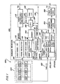
- FIG. 1 is a high-level block diagram of the signal processing system 100.
- An inboard receiver module 102 containing the requisite electronic control and processing circuitry is located inside the submarine.
- a lightweight array of fiber optic interferometric sensors 104 is located on the outside hull of the submarine. Each sensor in the array reacts to an incoming acoustic pressure wave by phase modulating a light signal 118 sent from a laser module 116 of the inboard receiver module 102. Modulated signals from different sensors, each operating at a different carrier frequency, are passively multiplexed onto a single fiber optic cable return signal 120 and sent back to the receiver 102. The channel signals are then demultiplexed and demodulated by the receiver 102.
- the inboard receiver 102 is connected to the submarine's power system (not shown) via a power connection 106.
- the inboard receiver 102 has a power distribution and conditioning block 112 to provide the necessary power requirements for the receiver components.
- Each input light signal 118 is generated by the corresponding laser module 116.
- Each laser module includes a laser 117, a phase modulator 119, a laser driver card 97 and a laser controller card 98.
- the laser 117 used in the preferred embodiment is a Model 125 200 mW Nd:YAG laser, available from Lightwave Electronics of Palo Alto, California.
- the phase modulator 119 is preferably a lithium niobate phase modulator.
- each laser 117 powers 56 sensors (channels), typically 28 channels on each side of the submarine.
- the laser 117 crystal is heated with the temperature level provided from a frequency synthesizer 142 ( Figure 1).
- the frequency synthesizer 142 controls the temperature of each laser 117 crystal separately, as is well known in the art, to produce laser outputs with eight different "colors" i.e., different wavelength nominally at 1319 nanometers, which are provided to the corresponding phase modulator 119a - 119h.
- each sensor array 104 On their way back to the receive end of the inboard receiver 102, all first channel outputs from each sensor array 104 are multiplexed together via a signal multiplexer 121. This is repeated for all the other 55 channels. Therefore, 56 fiber optic cable return signals 120 return from the sensor array 104, with each fiber carrying eight multiplexed signals. The multiplexed signal is then processed by a receiver card 122 ( Figure 1). Depending upon the number of sensors used, several receiver cards 122 may be needed.
- the frequency synthesizer 142 contains the master system clock and controls the operation of the laser module 116 by defining laser parameters, such as laser color, power, and temperature, provided to the laser module 116 on an amp/freq control line 146.
- the timing information is provided to the receiver card 122 via a signal timing line 144.
- a CPU 130 and an associated memory 140 provide system level control and status information to the component of receiver 102 via data lines 132, 138, 141.
- the CPU 130 has a VME interface 139, attached to a VME bus 138, which exists between the CPU 130 and the receiver card 122.
- the CPU 130 is connected to the frequency synthesizer 142 via a data line 141.
- the receiver card 122 demultiplexes and demodulates the retum signal 120 and outputs a signal to a beamformer card 124 which provides additional signal processing.
- a fiber channel card 126 provides the signal information to an external fiber bus 110.
- Each receiver card 122 processes the signals from 7 fiber return signals 120, wherein each fiber has eight laser channels, or a total of 56 channels from eight different sensor arrays 104.
- FIG 3 is a detailed block diagram of the receiver card 122 shown in Figure 1.
- the return signal ⁇ ( ⁇ (t)) 120, containing 8 channels, output by the acoustic sensor array 104 is input into a polarization diversity detector (PDD) 200.
- PDD polarization diversity detector
- An example of a PDD which has three outputs is described in U.S Patent No. 5,448,058, entitled "OPTICAL SIGNAL DETECTION APPARATUS AND METHOD FOR PREVENTING POLARIZATION SIGNAL FADING IN OPTICAL FIBER INTERFEROMETRIC SENSOR SYSTEMS.”
- a bi-cell or a two-output PDD is used.
- the PDD 200 and some other elements of the receiver card 122 prevent polarization signal fading in the return signal 120.
- the PDD 200 converts the photonic energy of the optical fiber return signal 120 into two separate electrical currents 200a, 200b via two photodiodes.
- each opto-receiver 202a, 202b a transimpedance amplifier converts the input current to a voltage, and a variable gain amplifier sets the voltage level in order to maximize the signal-to-noise level and to ensure that the voltage level is below the saturation level of ADCs 204a, 204b.
- the ADC used in the preferred embodiment has the part number 9042, and is manufactured by Analog Devices, Inc.
- the number of ADCs used is directly dependent upon the number of outputs from the PDD 200. Typically, there are two outputs, but three are possible.
- the digitized output contains a complex signal comprised of all channels on the return optical fiber return signal 120, which are the frequency division multiplexed phase generated carriers with the information-carrying sidebands.
- Each ADC 204a, 204b output is buffered and passed through to a multi-throw, multi-pole bus switch 206 which taps into each ADC 204a, 204b signal path.
- One output of the bus switch 206 goes to a digital down converter (DDC) 228, via signal path 238, which is employed as part of a calibration channel, as described below.
- the outputs of the bus switch 206 go to the signal channel DDCs 208a, 208b, 208n.
- the purpose of the bus switch 206 is to allow each of the DDCs 208 to be able to connect to any ADC output. This is required by the PDD 200 selection algorithm, discussed below with reference to Figure 7.
- Each DDC 208a, 208b, 208n acts as a digital demultiplexer by performing mix down and filtering of the digital information, separating one channel out of the composite signal.
- the DDC chip employed in the presently preferred embodiment is the GC4014 chip manufactured by Graychip, Inc. This particular device has 2-channel capability. In other embodiments, each chip may only have 1/2 or 1-channel capability. The number of DDCs needed depends upon the number of channels used in a given application. For example, if the return signal 120 has 8 multiplexed channels, then 4 2-channel DDC chips are needed. In the present embodiment, 28 2-channel DDCs (56 channels) are used per receiver card 122, but only one calibration DDC 228 and receiver card controller 226 are required, as described below. Thus, seven channel groups are needed to process all 56 multiplexed signals, with 8 channels per multiplexed array output signal.
- Each DDC 208a, 208b, 208n outputs both in-phase (I) and quadrature phase (Q) data words that represent the rectangular components of the phase signal from the bus switch 206.
- I and Q components from the DDCs 208a, 208b, 208n are time division multiplexed (TDM) onto separate I and Q buses.
- TDM time division multiplexed
- the I and Q components which define the same phase angle do not have the same frequency in the present invention. They are harmonics of the same frequency and one of these components is usually on the fundamental frequency and the other is on the first harmonic frequency.
- the output signal paths 210, 212 (which may be serial, unidirectional data paths or bi-directional data paths) output the I and Q 8-bit data words to a buffer 214 which buffers the words and also converts the 8 bit words into 16 bit words.
- the I and Q words from all of the DDCs 208 in a time sequence are then demodulated.
- the I and Q words are converted from Cartesian to polar form by the coordinate transformer 216 to obtain the magnitude and the phase angle in polar coordinates.
- the coordinate transformer 216 of the preferred embodiment is a TMC2330A chip manufactured by Raytheon Corp., but may be any similar device.
- the output of the coordinate transformer 216 is the instantaneous phase angle, whose change is directly related to the change in acoustic pressure of the acoustic signal from the environment, and whose rate of change is directly related to the frequency of the acoustic signal from the environment for a given fiber optic sensor.
- the channel-by-channel instantaneous phase angles are further processed in an acoustic signal processor 218, with integration and filtering algorithms, which is also attached to the VME bus 138.
- the output of the acoustic signal processor 218 may then be provided to a visual display, an oscilloscope, or to some other signal processing blocks, as desired.
- Two DACs 222, 224 provide I and Q signals which can be used for testing or viewing the output signal.
- the calibration procedure described in the above-mentioned US-A-6 134 281 uses the receiver card 122 fine tuning loop for calibration of the receiver card 122 components.
- the output 238 of the bus switch 206 is used to feed the calibration channel DDC 228. If there is more than one PDD 200, there will be more than one bus switch 206 feeding the calibration channel DDC 228, in a TDM manner.
- the calibration channel DDC 228 is set to mimic each signal channel in tum.
- the calibration channel provides a way to check PDD output selection, phase shift adjustment and I/Q balance on a per signal channel basis in a non-obtrusive way.
- the data is processed by the DDC 228 into I and Q words similar to the output of the signal channel DDCs 208a, 208b, 208n.
- the I and Q words are then processed by the receiver card controller 226 (a digital signal processor with its own RAM and ROM 232 memory) to extract the information necessary to determine channel performance.
- the receiver card controller 226 of the preferred embodiment is a ADSP 2181 manufactured by Analog Devices, Inc.
- the operation of the receiver card controller 226 is described with reference to the flowchart of Figure 4.
- the following steps are performed by software which is either stored in the system controller's ROM 232 or is downloaded by the system CPU 130 to the signal processor 226 DSP RAM upon system initialization.
- All interrupts are disabled at step 302.
- the receiver card controller 226 digital signal processing unit (DSP) is initialized at step 304, along with any associated RAM memory and the DDCs 208.
- the interrupts are then enabled at step 306.
- a signal channel and a calibration channel are selected at step 308.
- the best PDD signal is selected at step 310 by making the ADC selection for each signal channel. This PDD selection step is further described below with reference to Figure 7.
- a phase shift algorithm for the in-phase I component is performed at step 312, which is shown in detail in Figure 5.
- a phase shift algorithm for the Q component is performed at step 314, as shown in Figure 6.
- An I/Q balance algorithm is executed at step 316, which is shown in detail in Figure 8. Steps 308 - 316 are repeated for each channel, until all the channels have been calibrated. In one embodiment, calibration is performed only at system start-up. In the preferred embodiment, however, the calibration procedure continues for each DDC for as long as the system is operating. This results in a dynamic calibration system which unobtrusively calibrates the system while signal processing functions are unaffected.
- step 310) The procedure for selecting the best PDD signal (step 310) is illustrated by the flowchart of Figure 7.
- the first ADC 204a is selected, and I and Q data samples are obtained at step 604.
- a maximum I peak-to-peak value is calculated at step 606, when Q value is near zero.
- These 32 maximum I peak-to-peak values are averaged to determine the average maximum I peak-to-peak value. Similar process may be performed to determine the average maximum Q peak-to- peak value, when needed.
- the average maximum I peak-to-peak value determined at step 606 is then stored at step 608. Then the second ADC 204b is selected at step 610. and Q data samples are then obtained for the second ADC 204b at step 612. Again, an average maximum I peak-to-peak value is calculated at step 614, and this value is stored at step 616. The two stored average maximum I peak-to-peak values are then compared at step 618. The ADC 204 which produces the larger I peak- to-peak value is then selected (steps 620, 622). Since selecting different ADCs 204 will affect the I and Q signal levels symmetrically, only one signal (I or Q) needs to be examined in this procedure. The PDD 200 selection step is performed for each channel separately. Thus, different channels within DDC 208 may actually be using different ADC 204 inputs, which is why each DDC 208 needs to be connected to both ADCs 204.
- phase shift algorithms for the I component (step 312) and the Q component (step 314) are shown in Figures 5 and 6, respectively.
- the purpose of these algorithms is to compensate for the misalignment of the return signal 120 from the laser modules 116, and the internal receiver card 122 local oscillator signal in the DDC 208.
- the misalignment occurs due to the fact that the laser modules 116 and the receiver card 122 are all run by the same master clock from the frequency synthesizer 142.
- the adjustment is performed in the DDC 208.
- the algorithm determines the phase offset values that result in a maximum phase signal (I data) and quadrature phase signal (Q data) for each channel.
- phase shift algorithm is performed on the I and Q data.
- the outputs of the phase shift algorithms are an I-phase offset and a Q-phase offset, which are the offsets that result in maximum-amplitude I and Q signals.
- a selected phase increment is stored in the calibration DDC 228, and the I and Q data values are obtained.
- an average maximum peak-to-peak value for I component is calculated. In the present embodiment 32 samples are used, but, depending upon the application, either more or less samples may be used. If the I value calculated at step 406 is greater to or equal to a previously obtained average maximum peak-to-peak value, then a MAX I(n) peak-to-peak variable is set equal to the current I value, and the corresponding phase value is also saved at step 410. Otherwise, at step 412, the MAX I(n) variable is set equal to the previously obtained average maximum peak-to-peak value of I, and the corresponding phase value is saved.
- FIG 8 is a flowchart illustrating the I/Q balance algorithm (step 316 of Figure 4). This procedure is necessary in order to normalize the maximum and Q vectors and thus to minimize the errors in phase angle calculations.
- the current I and Q gain settings for the current signal channel are read and the I and Q data samples are obtained for the current channel.
- the I and Q values are compared. If I is greater than Q, then a new I gain is calcuiated at step 706. The new I gain value is made equal to the current I gain value multiplied by the quotient [Q/I]. If, however, I is not greater than Q, then a new Q gain value is calculated at step 708. The new Q gain value is made equal to the current Q gain value multiplied by the quotient [I/Q]. The determined gain values are then re-written to the DDC 208 of the current signal channel.
- control signal bus and the data bus for the DDCs 208 are separate.
- the control signal path between the DDCs 208 and the receiver card controller 226 is a separate bi-directional parallel bus.
- the data signals are output onto a separate serial bus.
- the background calibration operations are processed in parallel to the high speed signal data process flow.
- both high speed signal processing and background calibration processing can occur at the same time.
- both signal and control information share the same parallel bus, and, due to throughput limitations on the bus, the calibration routines are run only during startup or when there is a break in normal system operations.
- the described calibration technique only performs the fine tuning of the receiver card 122 components because its benefits are dependent on the parameters provided to the laser modules 116 during the initialization time.
- an improved calibration method usable with an inboard receiver with digital demodulation circuit and fiber optic interferometric sensor arrays.
- an algorithm for coarse calibration of laser systems which can be performed during the system initialization time.
- This and other objects of the present invention may be met by a coarse calibration technique for laser modules of a data acquisition module in a signal processing system.
- This coarse calibration technique is based on phase modulation of each laser module output signal, controlled by a CPU.
- phase modulation coefficient is calculated for each laser and used as the amplitude of a cosine wave signal for the laser module carrier frequency for phase modulation of the laser output signal.
- the phase modulation coefficient is determined from a global average I/Q ratio, calculated for all channels of the selected laser module, as an average of all I/Q ratios of in-phase and quadrature phase angle components of the signals returned from the sensors.
- the phase modulation coefficient for the selected laser module is determined empirically or by dividing the previously determined phase modulation coefficient by the previously determined global average I/Q ratio.
- the coarse calibration algorithm of the present invention is performed on the laser modules 116 of the inboard receiver 102 system with digital demodulation circuit and fiber optic interferometric sensor arrays 104, as shown in Figure 1, Figure 2 and Figure 3.
- the coarse calibration of the laser modules 116 is controlled by the CPU 130 and is performed only at the system initialization time, in cooperation with the fine tuning calibration method.
- some software code of the coarse calibration algorithm of the present invention is downloaded from the flash memory 140 of the CPU 130 to other cards of the inboard receiver 102, such as the receiver card 122 and the frequency synthesizer 142.
- the Frequency Synthesizer 142 includes a processor with the Laser Module Supervisor which sets the laser modules 116 to proper operating optical frequencies and laser module carrier frequencies.
- the CPU 130 has the rest of the software code with the coarse calibration algorithm.
- the CPU 130 is interfaced with a system control panel which is operated by a human operator. One of the commands entered by the operator is the inboard receiver commence initialization command. The operator receives the system status report from the CPU 130.
- the download of the calibration code to the frequency synthesizer 142 is accomplished via an RS-232 serial line 141.
- the CPU 130 VME backplane interface 139 is attached via a VME bus 138 to the receiver card VME interface 143, using an IDMA port on the receiver card controller ADSP-2181 card.
- the VME bus 138 is used for download from the CPU 130 to the receiver card 122 over the VME backplane interface 139.
- the initialization of the laser modules 116 is accomplished when the Turn on Laser command is sent from the CPU 130 to the frequency synthesizer 142.
- the set of laser coefficients is read from the laser module 116 EEPROM and sent to the frequency synthesizer 142.
- the laser coefficients contain data about the allowed and preferred frequency and temperature range for each laser 117.
- Each laser 117 powers 56 sensor channels of the array panel 104.
- the laser 117 crystal is heated to the designated temperature level, provided by a signal from the frequency synthesizer 142, in order to produce a laser optical output sine wave signal with the required "color".
- the carrier frequency w 0 also has to be provided by the frequency synthesizer 142 to the corresponding phase modulator 119a - 119h, in the form of a modulating cosine wave signal 99, to modulate the phase of the laser optical output signal 118.
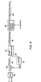
- FIG 9 is a block diagram illustrating a preferred configuration for the coarse calibration of a single laser module 117, according to the present invention.
- the frequency synthesizer 142 controls the operation of each laser 117 by providing, on the amp/freq control line 146 of Figure 1, the input cosine wave control signal 99 with the laser frequency w 0 (cos w 0 t) to the corresponding phase modulator 119, to modulate the phase of the laser optical output signal 118'.
- the frequency synthesizer 142 provides each laser controller card 98, and thus the corresponding phase modulator 119, with the appropriate phase modulation amplitude value "C", to control the phase of each laser optical output signal 118 in the coarse calibration loop of the inboard receiver 102.
- the I and Q components of the phase angle ⁇ (t) and their ratio I/Q are determined and optimized for each sensor channel at the appropriate receiver card 122 and receiver card controller 226, as described in the prior art. They are used both in the fine tuning algorithm of the prior art, performed on the receiver card 122, and in the coarse tuning algorithm of the present invention performed in the whole inboard receiver 102.
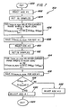
- FIG 10 is a flowchart illustrating the steps of the coarse calibration algorithm of the present invention, performed under control of the CPU 130 at the system initialization time.
- the next uncalibrated laser is selected.
- the steps of the coarse calibration algorithm are repeated iteratively for each laser, as long as is needed to obtain the I/Q ratio for each channel as close as possible to 1.0, at which time it is proclaimed at step 912 that all lasers controlled by that CPU are calibrated.
- the optimum values of the phase modulation coefficients for all laser modules controlled by that CPU are stored in the CPU 130 for the next initialization time.
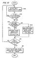
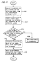
- FIG 11 is a flowchart illustrating the steps of the phase modulation coefficient determination module of the coarse calibration algorithm, performed for the selected laser according to the present invention.
- a command is sent to the appropriate receiver card(s) 122 receiver card controller 226 to collect the I/Q ratio value for each channel assigned to the selected laser, calculated from the average maximum I peak-to-peak and average maximum Q peak-to-peak values, and obtained according to the algorithm of Figure 3.
- the I/Q ratio is calculated for each channel as a ratio of an average maximum I value (i.e., when Q is near 0) divided by the average maximum Q value (i.e., when I is near 0), where the average I and Q values are taken from a predetermined number of samples for that channel. Therefore, the I/Q values calculated during the fine tuning calibration at the system initialization time, at the appropriate receiver card 122, are sent to the CPU 130 via its VME backplane interface 139.
- the collected values of I/Q ratio for all channels controlled by the selected laser are added, in order to determine a global average I/Q ratio for all the channels controlled by the selected laser.
- the sensor values which are out of tolerance are discarded.
- the new optimum value of the phase modulation coefficient for the selected laser may be determined empirically or by calculation. In the preferred embodiment of the present invention this value may be obtained by an appropriate mathematical algorithm performed in the CPU 130.
- the new value of the phase modulation coefficient for example, may be calculated by dividing the old value of the phase modulation coefficient by the old value of the global average I/Q ratio.
- the CPU 130 determines the optimum value of the phase modulation coefficient for each laser module 116.
- This coefficient is actually the optimum value of the phase modulation amplitude C of the cosine wave signal 99 supplied to the phase modulator 119 by the frequency synthesizer 142, as shown in Figure 8. It is possible that each sensor in the array panel 104 receives a slightly different signal from the assigned laser 117, so it is impossible to provide a perfect value for the phase modulation amplitude C which would be ideal for all sensors, but only a value optimal for most sensors. Therefore, each receiver card 122 channel has to be fine tuned, as described in the above mentioned prior art patent applications.
- each CPU 130 has a memory map from which it is determined which receiver cards 122, controlled by that CPU, are associated with the selected laser module 116.
- Each CPU 130 preferably controls eight lasers. Ideally, each CPU 130 assists all 56 channels of the laser module 116 when they are all received on the same receiver card 122. However, for practical reasons, in the implementation of the present invention each receiver card 122 assists only 28 channels of each laser module 116. Therefore, each array panel 104 sensor channels are divided between two CPUs and the memory map in this embodiment defines which CPU coarse calibration module would be used to perform the calibration of the whole array panel 104, based on data from the 28 channels assigned to that CPU. It is conceivable, however, that in another embodiment each CPU would calculate its own global average I/Q ratio and that the value closer to 1.0, or the average of the two values, would be chosen to determine the phase modulation amplitude C for that laser.
Landscapes
- Physics & Mathematics (AREA)
- General Physics & Mathematics (AREA)
- Biochemistry (AREA)
- Life Sciences & Earth Sciences (AREA)
- Chemical & Material Sciences (AREA)
- Analytical Chemistry (AREA)
- Health & Medical Sciences (AREA)
- General Health & Medical Sciences (AREA)
- Immunology (AREA)
- Pathology (AREA)
- Optical Communication System (AREA)
- Measurement Of Velocity Or Position Using Acoustic Or Ultrasonic Waves (AREA)
- Arrangements For Transmission Of Measured Signals (AREA)
- Testing Of Optical Devices Or Fibers (AREA)
- Lasers (AREA)
Description
- The present invention relates generally to the field of signal processing, and more specifically to a method and apparatus for calibration of a multi-channel fiber optic interferometric sensor system in a signal processing system.
- Acoustic listening systems for underwater applications are well known in the art. They are typically equipped with arrays of acoustic sensors which provide sensitive underwater listening capabilities and may provide relative position information. Each sensor reacts to an incoming pressure wave by modulating an input signal and the outputs of all the sensors are processed to determine the sound and position information. These sensor arrays are generally either attached to the submarine hull or are towed behind the submarine. Ideally, the sensors would be attached to the submarine hull, but prior art acoustic sensors were too heavy for many submarine applications. Recent advances in acoustic sensor array technology, however, have produced arrays which are light enough to be mounted on a submarine hull and which still provide very sensitive signal response. This weight reduction has also allowed the number of sensors to be increased.
- Another application for underwater acoustic sensors is in the geological survey industry, specifically, for underwater oil exploration. Vast arrays of sensors may be placed on the ocean bottom in the vicinity of known oil reserves. A surface ship initiates an acoustic pressure wave with a large air burst. The acoustic pressure wave and its reflection off the ocean floor are detected by the sensor arrays. The data from the sensors is then processed and analyzed to determine optimum drilling locations or to monitor the status of known reservoirs.
- As the number and complexity of the acoustic sensors in these and related applications have increased, the associated signal processing electronics modules have likewise increased. Typical conventional systems use analog circuitry to interrogate the sensors, but these analog systems are subject to drift and it is very difficult to accurately calibrate them. Recent developments have provided fiber optic interferometric sensors, as described in the article "Homodyne Demodulation Scheme for Fiber Optic Sensors Using Phase Generated Carrier" by Anthony Dandridge, Alan B. Tveten, and Thomas G. Giallorenzi, IEEE Journal of Quantum Electronics, Vol. QE-18, No. 10, October 1982. This reference teaches a modulation/demodulation technique in which the frequencies of I and Q components are different, which is employed in the present invention.
- The above-mentioned related patent applications describe techniques for interrogation of fiber optic interferometric sensors in multi-channel applications and for fine tuning of a
receiver card 122 by calibration of digital down converters of thesignal processing system 100 of Figure 1. Thesignal processing system 100 is comprised of a source end with lasers, sensors and control electronics, and a receive end. The sensors are located in-between the source end and receive end as part of the outboard telemetry. The sensors are fiber optic sensors which get the information from the environment sensed by the fiber optic interferometers. The optical fiber interferometer has a reference fiber and a signal fiber. A relative optical phase shift between these two fibers is the information returned by the telemetry and extracted by the receive end. - Figure 1 is a high-level block diagram of the
signal processing system 100. An inboard receiver module 102 containing the requisite electronic control and processing circuitry is located inside the submarine. A lightweight array of fiber opticinterferometric sensors 104 is located on the outside hull of the submarine. Each sensor in the array reacts to an incoming acoustic pressure wave by phase modulating alight signal 118 sent from alaser module 116 of the inboard receiver module 102. Modulated signals from different sensors, each operating at a different carrier frequency, are passively multiplexed onto a single fiber opticcable return signal 120 and sent back to the receiver 102. The channel signals are then demultiplexed and demodulated by the receiver 102. - The inboard receiver 102 is connected to the submarine's power system (not shown) via a
power connection 106. The inboard receiver 102 has a power distribution andconditioning block 112 to provide the necessary power requirements for the receiver components. Eachinput light signal 118 is generated by thecorresponding laser module 116. Each laser module includes alaser 117, aphase modulator 119, alaser driver card 97 and alaser controller card 98. Thelaser 117 used in the preferred embodiment is aModel 125 200 mW Nd:YAG laser, available from Lightwave Electronics of Palo Alto, California. Thephase modulator 119 is preferably a lithium niobate phase modulator. - As shown in Figure 2, eight laser modules with eight lasers 117a-117h drive eight corresponding sensor arrays 104a - 104h. Each
laser 117powers 56 sensors (channels), typically 28 channels on each side of the submarine. Thelaser 117 crystal is heated with the temperature level provided from a frequency synthesizer 142 (Figure 1). Thefrequency synthesizer 142 controls the temperature of eachlaser 117 crystal separately, as is well known in the art, to produce laser outputs with eight different "colors" i.e., different wavelength nominally at 1319 nanometers, which are provided to thecorresponding phase modulator 119a - 119h. - On their way back to the receive end of the inboard receiver 102, all first channel outputs from each
sensor array 104 are multiplexed together via a signal multiplexer 121. This is repeated for all the other 55 channels. Therefore, 56 fiber opticcable return signals 120 return from thesensor array 104, with each fiber carrying eight multiplexed signals. The multiplexed signal is then processed by a receiver card 122 (Figure 1). Depending upon the number of sensors used,several receiver cards 122 may be needed. - The
frequency synthesizer 142 contains the master system clock and controls the operation of thelaser module 116 by defining laser parameters, such as laser color, power, and temperature, provided to thelaser module 116 on an amp/freq control line 146. The timing information is provided to thereceiver card 122 via asignal timing line 144. ACPU 130 and an associatedmemory 140 provide system level control and status information to the component of receiver 102 viadata lines CPU 130 has aVME interface 139, attached to aVME bus 138, which exists between theCPU 130 and thereceiver card 122. TheCPU 130 is connected to thefrequency synthesizer 142 via adata line 141. - The
receiver card 122 demultiplexes and demodulates theretum signal 120 and outputs a signal to abeamformer card 124 which provides additional signal processing. Afiber channel card 126 provides the signal information to anexternal fiber bus 110. Eachreceiver card 122, processes the signals from 7fiber return signals 120, wherein each fiber has eight laser channels, or a total of 56 channels from eightdifferent sensor arrays 104. - Figure 3 is a detailed block diagram of the
receiver card 122 shown in Figure 1. The return signal λ((t)) 120, containing 8 channels, output by theacoustic sensor array 104 is input into a polarization diversity detector (PDD) 200. An example of a PDD which has three outputs is described in U.S Patent No. 5,448,058, entitled "OPTICAL SIGNAL DETECTION APPARATUS AND METHOD FOR PREVENTING POLARIZATION SIGNAL FADING IN OPTICAL FIBER INTERFEROMETRIC SENSOR SYSTEMS." In the preferred embodiment, a bi-cell or a two-output PDD is used. ThePDD 200 and some other elements of thereceiver card 122 prevent polarization signal fading in thereturn signal 120. The PDD 200 converts the photonic energy of the opticalfiber return signal 120 into two separateelectrical currents - In each opto-
receiver ADCs receivers ADCs receivers - The number of ADCs used is directly dependent upon the number of outputs from the
PDD 200. Typically, there are two outputs, but three are possible. At this point, the digitized output contains a complex signal comprised of all channels on the return opticalfiber return signal 120, which are the frequency division multiplexed phase generated carriers with the information-carrying sidebands. - Each
ADC multi-pole bus switch 206 which taps into eachADC bus switch 206 goes to a digital down converter (DDC) 228, viasignal path 238, which is employed as part of a calibration channel, as described below. The outputs of thebus switch 206 go to thesignal channel DDCs bus switch 206 is to allow each of the DDCs 208 to be able to connect to any ADC output. This is required by thePDD 200 selection algorithm, discussed below with reference to Figure 7. - Each
DDC return signal 120 has 8 multiplexed channels, then 4 2-channel DDC chips are needed. In the present embodiment, 28 2-channel DDCs (56 channels) are used perreceiver card 122, but only onecalibration DDC 228 andreceiver card controller 226 are required, as described below. Thus, seven channel groups are needed to process all 56 multiplexed signals, with 8 channels per multiplexed array output signal. - Each
DDC bus switch 206. These I and Q components from theDDCs output signal paths 210, 212 (which may be serial, unidirectional data paths or bi-directional data paths) output the I and Q 8-bit data words to abuffer 214 which buffers the words and also converts the 8 bit words into 16 bit words. - The I and Q words from all of the DDCs 208 in a time sequence are then demodulated. The I and Q words are converted from Cartesian to polar form by the coordinate
transformer 216 to obtain the magnitude and the phase angle in polar coordinates. The coordinatetransformer 216 of the preferred embodiment is a TMC2330A chip manufactured by Raytheon Corp., but may be any similar device. - The output of the coordinate
transformer 216 is the instantaneous phase angle, whose change is directly related to the change in acoustic pressure of the acoustic signal from the environment, and whose rate of change is directly related to the frequency of the acoustic signal from the environment for a given fiber optic sensor. The channel-by-channel instantaneous phase angles are further processed in anacoustic signal processor 218, with integration and filtering algorithms, which is also attached to theVME bus 138. The output of theacoustic signal processor 218 may then be provided to a visual display, an oscilloscope, or to some other signal processing blocks, as desired. TwoDACs - The calibration procedure described in the above-mentioned US-
A-6 134 281 uses thereceiver card 122 fine tuning loop for calibration of thereceiver card 122 components. For that purpose theoutput 238 of thebus switch 206 is used to feed thecalibration channel DDC 228. If there is more than onePDD 200, there will be more than onebus switch 206 feeding thecalibration channel DDC 228, in a TDM manner. Thecalibration channel DDC 228 is set to mimic each signal channel in tum. The calibration channel provides a way to check PDD output selection, phase shift adjustment and I/Q balance on a per signal channel basis in a non-obtrusive way. For that purpose, the data is processed by theDDC 228 into I and Q words similar to the output of thesignal channel DDCs ROM 232 memory) to extract the information necessary to determine channel performance. Thereceiver card controller 226 of the preferred embodiment is aADSP 2181 manufactured by Analog Devices, Inc. - The operation of the
receiver card controller 226 is described with reference to the flowchart of Figure 4. The following steps are performed by software which is either stored in the system controller'sROM 232 or is downloaded by thesystem CPU 130 to thesignal processor 226 DSP RAM upon system initialization. Upon power initialization or asystem reinitialization 300, all interrupts are disabled atstep 302. Thereceiver card controller 226 digital signal processing unit (DSP) is initialized atstep 304, along with any associated RAM memory and the DDCs 208. The interrupts are then enabled atstep 306. A signal channel and a calibration channel are selected atstep 308. Then, the best PDD signal is selected atstep 310 by making the ADC selection for each signal channel. This PDD selection step is further described below with reference to Figure 7. - A phase shift algorithm for the in-phase I component is performed at
step 312, which is shown in detail in Figure 5. Similarly, a phase shift algorithm for the Q component is performed atstep 314, as shown in Figure 6. An I/Q balance algorithm is executed atstep 316, which is shown in detail in Figure 8. Steps 308 - 316 are repeated for each channel, until all the channels have been calibrated. In one embodiment, calibration is performed only at system start-up. In the preferred embodiment, however, the calibration procedure continues for each DDC for as long as the system is operating. This results in a dynamic calibration system which unobtrusively calibrates the system while signal processing functions are unaffected. - The procedure for selecting the best PDD signal (step 310) is illustrated by the flowchart of Figure 7. At
step 602, thefirst ADC 204a is selected, and I and Q data samples are obtained atstep 604. A maximum Ipeak-to-peak value is calculated atstep 606, when Q value is near zero. When Q=0, the Ipeak-to-peak has maximum value but it is difficult to catch that moment. Therefore, a set of I values is collected of points within an interval around the time when Q=0. There are preferably 32 collected I values when the Ipeak-to-peak values are at their maximum Ipeak-to-peak value. These 32 maximum Ipeak-to-peak values are averaged to determine the average maximum Ipeak-to-peak value. Similar process may be performed to determine the average maximum Qpeak-to- peak value, when needed. - The average maximum Ipeak-to-peak value determined at
step 606 is then stored atstep 608. Then thesecond ADC 204b is selected at step 610. and Q data samples are then obtained for thesecond ADC 204b atstep 612. Again, an average maximum Ipeak-to-peak value is calculated atstep 614, and this value is stored atstep 616. The two stored average maximum Ipeak-to-peak values are then compared atstep 618. The ADC 204 which produces the larger Ipeak- to-peak value is then selected (steps 620, 622). Since selecting different ADCs 204 will affect the I and Q signal levels symmetrically, only one signal (I or Q) needs to be examined in this procedure. ThePDD 200 selection step is performed for each channel separately. Thus, different channels within DDC 208 may actually be using different ADC 204 inputs, which is why each DDC 208 needs to be connected to both ADCs 204. - The phase shift algorithms for the I component (step 312) and the Q component (step 314) are shown in Figures 5 and 6, respectively. The purpose of these algorithms is to compensate for the misalignment of the return signal 120 from the
laser modules 116, and theinternal receiver card 122 local oscillator signal in the DDC 208. The misalignment occurs due to the fact that thelaser modules 116 and thereceiver card 122 are all run by the same master clock from thefrequency synthesizer 142. The adjustment is performed in the DDC 208. The algorithm determines the phase offset values that result in a maximum phase signal (I data) and quadrature phase signal (Q data) for each channel. This is accomplished by successively programming the calibration DDC's phase offset control registers with equal phase increments and reading the corresponding I and Q data from the channel output registers. The I and Q data generated by thecalibration DDC 228 are read by thereceiver card controller 226 and stored into two separate buffers. Once a sufficient number of data samples has been accumulated, the phase shift algorithm is performed on the I and Q data. The outputs of the phase shift algorithms are an I-phase offset and a Q-phase offset, which are the offsets that result in maximum-amplitude I and Q signals. These optimal offset values are then stored in the associated signal channel DDC. - At step 404 a selected phase increment is stored in the
calibration DDC 228, and the I and Q data values are obtained. Atstep 406 an average maximum peak-to-peak value for I component is calculated. In thepresent embodiment 32 samples are used, but, depending upon the application, either more or less samples may be used. If the I value calculated atstep 406 is greater to or equal to a previously obtained average maximum peak-to-peak value, then a MAX I(n)peak-to-peak variable is set equal to the current I value, and the corresponding phase value is also saved atstep 410. Otherwise, atstep 412, the MAX I(n) variable is set equal to the previously obtained average maximum peak-to-peak value of I, and the corresponding phase value is saved. - This procedure is repeated at
step 402 until all I phase increments have been tested. The resulting MAX I(n) value is then stored into the corresponding DDC chip associated with the current channel. The procedure for determining the Q phase shift value, shown in Figure 6, is exactly the same as the procedure for determining the I phase shift value, as shown in Figure 5. These algorithms which provide the calculated phase offsets are utilized to move the starting point of the DDC 208 oscillator signal until it is aligned with the received carrier signal, as it enters the DDC 208, to keep the signals in phase. - Figure 8 is a flowchart illustrating the I/Q balance algorithm (step 316 of Figure 4). This procedure is necessary in order to normalize the maximum and Q vectors and thus to minimize the errors in phase angle calculations. At
step 700, the current I and Q gain settings for the current signal channel are read and the I and Q data samples are obtained for the current channel. Atstep 704, the I and Q values are compared. If I is greater than Q, then a new I gain is calcuiated atstep 706. The new I gain value is made equal to the current I gain value multiplied by the quotient [Q/I]. If, however, I is not greater than Q, then a new Q gain value is calculated atstep 708. The new Q gain value is made equal to the current Q gain value multiplied by the quotient [I/Q]. The determined gain values are then re-written to the DDC 208 of the current signal channel. - In the preferred embodiment, the control signal bus and the data bus for the DDCs 208 are separate. The control signal path between the DDCs 208 and the
receiver card controller 226 is a separate bi-directional parallel bus. The data signals are output onto a separate serial bus. By using different buses to move data into and out of the DDCs 208, the background calibration operations are processed in parallel to the high speed signal data process flow. As a result, both high speed signal processing and background calibration processing can occur at the same time. In another embodiment, both signal and control information share the same parallel bus, and, due to throughput limitations on the bus, the calibration routines are run only during startup or when there is a break in normal system operations. - However, the described calibration technique only performs the fine tuning of the
receiver card 122 components because its benefits are dependent on the parameters provided to thelaser modules 116 during the initialization time. Thus, there is a need for an improved calibration method usable with an inboard receiver with digital demodulation circuit and fiber optic interferometric sensor arrays. Specifically, there is a need for an algorithm for coarse calibration of laser systems, which can be performed during the system initialization time. - It is thus an object of the present invention to provide an apparatus and method for comprehensive calibration of laser modules in a signal processing system.
- This and other objects of the present invention may be met by a coarse calibration technique for laser modules of a data acquisition module in a signal processing system. This coarse calibration technique is based on phase modulation of each laser module output signal, controlled by a CPU.
- An optimal value of a phase modulation coefficient is calculated for each laser and used as the amplitude of a cosine wave signal for the laser module carrier frequency for phase modulation of the laser output signal. The phase modulation coefficient is determined from a global average I/Q ratio, calculated for all channels of the selected laser module, as an average of all I/Q ratios of in-phase and quadrature phase angle components of the signals returned from the sensors. The phase modulation coefficient for the selected laser module is determined empirically or by dividing the previously determined phase modulation coefficient by the previously determined global average I/Q ratio.
- The exact nature of this invention, as well as its objects and advantages, will become readily apparent from consideration of the following specification as illustrated in the accompanying drawings, in which like reference numerals designate like parts throughout the figures thereof, and wherein:
- Figure 1 is a high-level block diagram of a signal processing system with digital demodulation circuit used with the present invention;
- Figure 2 is a block diagram illustrating a preferred configuration for an inboard receiver with laser modules driving sensor arrays;
- Figure 3 is a detailed hardware block diagram of the receiver of Figure 1;
- Figure 4 is a flowchart illustrating the operation of the system controller;
- Figure 5 is flowchart illustrating the phase shift algorithm for the in-phase signal (I data);
- Figure 6 is a flowchart illustrating the phase shift algorithm for the quadrature phase signal (Q data);
- Figure 7 is a flowchart illustrating the functional flow of the polarization diversity detector (PDD) selection procedure;
- Figure 8 is a flowchart illustrating the I/Q balance algorithm;
- Figure 9 is a block diagram illustrating a preferred configuration for obtaining coarse calibration of a single laser module, according to the present invention;
- Figure 10 is a flowchart illustrating the steps of the coarse calibration algorithm, according to the present invention; and
- Figure 11 is a flowchart illustrating the steps of the phase modulation coefficient determination module of the coarse calibration algorithm, according to the present invention.
-
- The following description is provided to enable any person skilled in the art to make and use the invention and sets forth the best modes contemplated by the inventor for carrying out the invention. Various modifications, however, will remain readily apparent to those skilled in the art, since the basic principles of the present invention have been defined herein specifically to provide a method and apparatus for coarse calibration of laser modules in a data acquisition and signal processing system, based on phase modulation.
- The coarse calibration algorithm of the present invention is performed on the
laser modules 116 of the inboard receiver 102 system with digital demodulation circuit and fiber opticinterferometric sensor arrays 104, as shown in Figure 1, Figure 2 and Figure 3. Preferably, the coarse calibration of thelaser modules 116 is controlled by theCPU 130 and is performed only at the system initialization time, in cooperation with the fine tuning calibration method. - At the initialization time, some software code of the coarse calibration algorithm of the present invention, including the data input/output protocol routines, is downloaded from the
flash memory 140 of theCPU 130 to other cards of the inboard receiver 102, such as thereceiver card 122 and thefrequency synthesizer 142. TheFrequency Synthesizer 142 includes a processor with the Laser Module Supervisor which sets thelaser modules 116 to proper operating optical frequencies and laser module carrier frequencies. TheCPU 130 has the rest of the software code with the coarse calibration algorithm. TheCPU 130 is interfaced with a system control panel which is operated by a human operator. One of the commands entered by the operator is the inboard receiver commence initialization command. The operator receives the system status report from theCPU 130. - The download of the calibration code to the
frequency synthesizer 142 is accomplished via an RS-232serial line 141. TheCPU 130VME backplane interface 139 is attached via aVME bus 138 to the receiver card VME interface 143, using an IDMA port on the receiver card controller ADSP-2181 card. TheVME bus 138 is used for download from theCPU 130 to thereceiver card 122 over theVME backplane interface 139. - The initialization of the
laser modules 116 is accomplished when the Turn on Laser command is sent from theCPU 130 to thefrequency synthesizer 142. For eachlaser module 116, the set of laser coefficients is read from thelaser module 116 EEPROM and sent to thefrequency synthesizer 142. The laser coefficients contain data about the allowed and preferred frequency and temperature range for eachlaser 117. After the verification of thelaser modules 116 status, which should have proper voltages and currents, is received in theCPU 130 from thefrequency synthesizer 142, the startup of theinternal CPU 130 timer is used for the warm-up of thelasers 117. - Each
laser 117powers 56 sensor channels of thearray panel 104. Thelaser 117 crystal is heated to the designated temperature level, provided by a signal from thefrequency synthesizer 142, in order to produce a laser optical output sine wave signal with the required "color". The carrier frequency w0 also has to be provided by thefrequency synthesizer 142 to thecorresponding phase modulator 119a - 119h, in the form of a modulatingcosine wave signal 99, to modulate the phase of the laseroptical output signal 118. - Figure 9 is a block diagram illustrating a preferred configuration for the coarse calibration of a
single laser module 117, according to the present invention. Thefrequency synthesizer 142 controls the operation of eachlaser 117 by providing, on the amp/freq control line 146 of Figure 1, the input cosinewave control signal 99 with the laser frequency w0 (cos w0t) to thecorresponding phase modulator 119, to modulate the phase of the laser optical output signal 118'. In addition, thefrequency synthesizer 142 provides eachlaser controller card 98, and thus thecorresponding phase modulator 119, with the appropriate phase modulation amplitude value "C", to control the phase of each laseroptical output signal 118 in the coarse calibration loop of the inboard receiver 102. - The phase modulation amplitude value "C" is calculated in the
CPU 130, according to the algorithm described below and shown in Figures 10 and 11. Therefore, the signal provided to the phase modulator 119 (C.cos w0t) is used to modulate the phase of the correspondinglaser output signal 118 to provide theoutput light signal 118 with the intensity I = A + B'.cos(C.cos w0t). The phase of this signal is further phase modulated in eachinterferometric sensor 95 of thearray panel 104, as described in the above-mentioned article by Dandridge et al., to obtain thereturn signal 120 with the intensity I = A + B.cos(C.cos w0t + (t)). Eachinterferometric sensor 95 introduces the change in intensity from B' to B, dependent on the mixing efficiency of theinterferometric sensor 95, and the phase angle (t) = wt + ψ (t). - The I and Q components of the phase angle (t) and their ratio I/Q are determined and optimized for each sensor channel at the
appropriate receiver card 122 andreceiver card controller 226, as described in the prior art. They are used both in the fine tuning algorithm of the prior art, performed on thereceiver card 122, and in the coarse tuning algorithm of the present invention performed in the whole inboard receiver 102. - Figure 10 is a flowchart illustrating the steps of the coarse calibration algorithm of the present invention, performed under control of the
CPU 130 at the system initialization time. Atstep 902 the next uncalibrated laser is selected. After it is determined instep 904 that the selected laser is properly started, atstep 906 it is verified whether this is the first calibration attempt for the selectedlaser 117. If it is so, the stored optimum phase modulation coefficient value is sent to the selected laser, via thefrequency synthesizer 142, atstep 908. Otherwise, the phase modulation coefficient determination routine of Figure 10 is invoked atstep 910. The steps of the coarse calibration algorithm are repeated iteratively for each laser, as long as is needed to obtain the I/Q ratio for each channel as close as possible to 1.0, at which time it is proclaimed atstep 912 that all lasers controlled by that CPU are calibrated. Atstep 914 the optimum values of the phase modulation coefficients for all laser modules controlled by that CPU are stored in theCPU 130 for the next initialization time. - Figure 11 is a flowchart illustrating the steps of the phase modulation coefficient determination module of the coarse calibration algorithm, performed for the selected laser according to the present invention. At step 1002 a command is sent to the appropriate receiver card(s) 122
receiver card controller 226 to collect the I/Q ratio value for each channel assigned to the selected laser, calculated from the average maximum Ipeak-to-peak and average maximum Qpeak-to-peak values, and obtained according to the algorithm of Figure 3. The I/Q ratio is calculated for each channel as a ratio of an average maximum I value (i.e., when Q is near 0) divided by the average maximum Q value (i.e., when I is near 0), where the average I and Q values are taken from a predetermined number of samples for that channel. Therefore, the I/Q values calculated during the fine tuning calibration at the system initialization time, at theappropriate receiver card 122, are sent to theCPU 130 via itsVME backplane interface 139. - At
step 1004, performed in theCPU 130, the collected values of I/Q ratio for all channels controlled by the selected laser are added, in order to determine a global average I/Q ratio for all the channels controlled by the selected laser. The sensor values which are out of tolerance are discarded. Atstep 1006 it is verified whether the new global average I/Q ratio is better than the previous global average I/Q ratio. If it is determined that it is better and that the obtained value is close enough to 1.0 (within appropriate tolerance level presently set to 0.01), the laser status is set to the calibrated flag atstep 1008 and the routine exits. If it is not better, a new optimum value of the phase modulation coefficient for the selected laser is determined atstep 1010 and it is sent to the selected laser atstep 1012. - At
step 1010, the new optimum value of the phase modulation coefficient for the selected laser may be determined empirically or by calculation. In the preferred embodiment of the present invention this value may be obtained by an appropriate mathematical algorithm performed in theCPU 130. The new value of the phase modulation coefficient, for example, may be calculated by dividing the old value of the phase modulation coefficient by the old value of the global average I/Q ratio. - Therefore, according to the steps of the coarse calibration algorithm of the present invention the
CPU 130 determines the optimum value of the phase modulation coefficient for eachlaser module 116. This coefficient is actually the optimum value of the phase modulation amplitude C of thecosine wave signal 99 supplied to thephase modulator 119 by thefrequency synthesizer 142, as shown in Figure 8. It is possible that each sensor in thearray panel 104 receives a slightly different signal from the assignedlaser 117, so it is impossible to provide a perfect value for the phase modulation amplitude C which would be ideal for all sensors, but only a value optimal for most sensors. Therefore, eachreceiver card 122 channel has to be fine tuned, as described in the above mentioned prior art patent applications. - In one embodiment of the present invention each
CPU 130 has a memory map from which it is determined whichreceiver cards 122, controlled by that CPU, are associated with the selectedlaser module 116. EachCPU 130 preferably controls eight lasers. Ideally, eachCPU 130 assists all 56 channels of thelaser module 116 when they are all received on thesame receiver card 122. However, for practical reasons, in the implementation of the present invention eachreceiver card 122 assists only 28 channels of eachlaser module 116. Therefore, eacharray panel 104 sensor channels are divided between two CPUs and the memory map in this embodiment defines which CPU coarse calibration module would be used to perform the calibration of thewhole array panel 104, based on data from the 28 channels assigned to that CPU. It is conceivable, however, that in another embodiment each CPU would calculate its own global average I/Q ratio and that the value closer to 1.0, or the average of the two values, would be chosen to determine the phase modulation amplitude C for that laser. - Those skilled in the art will appreciate that various adaptations and modifications of the just-described preferred embodiments can be configured without departing from the scope of the invention. Therefore, it is to be understood that within the scope of the appended claims, the invention may be practiced other than as specifically described herein. For example, in addition to the above mentioned underwater applications the present invention is also applicable to commercial and military seismic applications.
Claims (13)
- A calibration method for laser modules in a signal processing system, comprising the steps of:selecting a laser module to be calibrated;determining if the selected laser module has been calibrated before;if not calibrated before, sending a saved phase modulation amplitude value to the selected laser module to be used for phase modulation of the laser module output signal;if calibrated before, determining a new phase modulation amplitude value from a determined in-phase and quadrature phase (I/Q) ratio of the channel assigned to the laser module, for phase modulation of the laser module output signal;repeating the above steps for each laser module in the signal processing system until all laser modules are calibrated; andsaving the new phase modulation amplitude values for all laser modules.
- The method of claim 1, wherein the, step of determining the new phase modulation amplitude value further comprises the steps of:obtaining ratios of in-phase and quadrature phase angle components (I/Q) ratios for all channels of the selected laser module;calculating a new global average I/Q ratio for all channels of the selected laser module as an average of all said I/Q ratios;comparing the new global average I/Q ratio with the previously determined global average I/Q ratio; andif the new global average I/Q ratio is closer to 1 than the previously determined global average I/Q ratio and within a predetermined tolerance, giving the selected laser module a calibrated status, orif the new global average I/Q ratio is not closer to 1 than the previously determined global average I/Q ratio or not within the predetermined tolerance, determining a new phase modulation amplitude value for the selected laser module; andsending the new phase modulation amplitude value to the selected laser module to be used for phase modulation of the laser module output signal as the amplitude of a cosine wave signal with the laser module carrier frequency.
- The method of claim 1 or claim 2, wherein the step of determining the new phase modulation amplitude value for the selected laser module performs determination by an empirical method.
- The method of claim 1 or claim 2, wherein the step of determining the new phase modulation amplitude value for the selected laser module further comprises the step of:obtaining the new phase modulation amplitude value by dividing the previously determined phase modulation amplitude value by a previously determined global average I/Q ratio.
- The method of any of claims 2 to 4 when dependent upon claim 2, wherein the step of obtaining ratios of in-phase and quadrature phase angle components (I/Q ratios) for all channels of the selected laser module further comprises the steps of:calculating an average maximum value for an in-phase component of a phase angle received for the channel;calculating an average maximum value for a quadrature component of the phase angle received for the channel;dividing the calculated average maximum value for the in-phase component of the phase angle with the calculated average maximum value for the quadrature component of the phase angle; andrepeating the above steps for each channel of the selected laser module.
- The method of claim 5, wherein the step of calculating the average maximum value for the in-phase component of the phase angle further comprises the steps of:obtaining a plurality of maximum peak-to-peak values of the in-phase component, taken when the quadrature component is near or at zero; andcalculating the average maximum value for said in-phase component from the plurality of maximum peak-to-peak values of the in-phase component.
- The method of claim 5 or claim 6, wherein the step of calculating the average maximum value for the quadrature component of the phase angle further comprises the steps of:obtaining a plurality of maximum peak-to-peak values of the quadrature component, taken when the in-phase component is near or at zero; andcalculating the average maximum value for said quadrature component from the plurality of maximum peak-to-peak values of the quadrature component.
- An apparatus for calibrating a laser module in a signal processing system, the apparatus comprising:at the carrier frequency and at the amplitude of the phase modulation amplitude value, the cosine wave signal being used for phase modulation of the laser module optical output signal.at least one laser module (117) for sending an output light signal to an associated array of sensor channels; andat least one receiver (122) for receiving return signals from each of the sensor channels, the return signals having an in-phase component and a quadrature component of a phase angle, the apparatus comprising:a system processor (130) adapted to receive the return signals from the sensor channels and perform the steps of:selecting a laser module to be calibrated;determining if the selected laser module has been calibrated before;if not calibrated before, sending a saved phase modulation amplitude value to the selected laser module to be used for phase modulation of the laser module output signal;if calibrated before, determining a new phase modulation amplitude value from a determined in-phase and quadrature phase (I/Q) ratio of the channel assigned to the laser module, for phase modulation of the laser module output signal;repeating the above steps for each laser module in the signal processing system until all laser modules are calibrated; andsaving the new phase modulation amplitude values for all laser modules; anda phase modulator for receiving a cosine wave signal
- The apparatus of claim 8 wherein said phase modulation amplitude value is dependent on a global average I/Q ratio, calculated for all the sensor channels of the laser module, wherein said global average I/Q ratio is calculated as an average of the ratios of the in-phase and quadrature phase angle component (I/Q) received for all sensor channels of the laser module.
- The apparatus of claim 8 or claim 9, wherein said phase modulation amplitude value is determined empirically.
- The apparatus of claim 8 or claim 9, wherein said phase modulation amplitude value is calculated by dividing the previously determined phase modulation amplitude value by the previously determined global average I/Q ratio.
- The apparatus of any of claims 8 to 11, wherein each said ratio of in-phase and quadrature phase angle component (I/Q ratio) is determined in the appropriate receiver, which calculates an average maximum value for an in-phase component of a phase angle and divides it with an average maximum value for a quadrature component of the phase angle.
- The apparatus of claim 12, wherein the average maximum value for the in-phase component of the phase angle is calculated as an average of a plurality of maximum peak-to-peak values of the in-phase component, taken when the quadrature component is near or at zero, and
the average maximum value for the quadrature component of the phase angle is calculated as an average of a plurality of maximum peak-to-peak values of the quadrature component, taken when the in-phase component is near or at zero.
Applications Claiming Priority (4)
| Application Number | Priority Date | Filing Date | Title |
|---|---|---|---|
| US74781 | 1993-06-10 | ||
| US7427398P | 1998-02-10 | 1998-02-10 | |
| US74273P | 1998-02-10 | ||
| US09/074,781 US6008900A (en) | 1998-02-10 | 1998-05-08 | Method and apparatus for calibration of a multi-channel fiber optic interferometric sensor system in a signal processing system |
Publications (3)
| Publication Number | Publication Date |
|---|---|
| EP0936452A2 EP0936452A2 (en) | 1999-08-18 |
| EP0936452A3 EP0936452A3 (en) | 2000-07-12 |
| EP0936452B1 true EP0936452B1 (en) | 2004-12-08 |
Family
ID=26755456
Family Applications (1)
| Application Number | Title | Priority Date | Filing Date |
|---|---|---|---|
| EP99300974A Expired - Lifetime EP0936452B1 (en) | 1998-02-10 | 1999-02-10 | Method and apparatus for calibration of a multi-channel fiber optic interferometric sensor system in a signal processing system |
Country Status (8)
| Country | Link |
|---|---|
| US (1) | US6008900A (en) |
| EP (1) | EP0936452B1 (en) |
| KR (1) | KR19990072555A (en) |
| AU (1) | AU740040B2 (en) |
| CA (1) | CA2259527A1 (en) |
| DE (1) | DE69922426T2 (en) |
| IL (1) | IL128451A (en) |
| NO (1) | NO322356B1 (en) |
Families Citing this family (14)
| Publication number | Priority date | Publication date | Assignee | Title |
|---|---|---|---|---|
| CA2313469C (en) * | 1997-12-17 | 2004-11-02 | James C. O'meara | Laser lighting system |
| US6600586B1 (en) * | 1999-05-10 | 2003-07-29 | Northrop Grumman Corporation | Normalization method for acquiring interferometer phase shift from frequency division multiplexed fiber optic sensor arrays |
| JP3903105B2 (en) * | 2000-05-23 | 2007-04-11 | 富士フイルム株式会社 | Dynamic change detection method, dynamic change detection apparatus, and ultrasonic diagnostic apparatus |
| EP1405444B1 (en) * | 2001-07-09 | 2013-01-23 | TQ Gamma, LLC | Fiber optic telecommunications card with security detection |
| US7346313B2 (en) | 2002-03-04 | 2008-03-18 | Cafarella John H | Calibration of I-Q balance in transceivers |
| US7038785B2 (en) | 2003-07-09 | 2006-05-02 | Northrop Grumman Corporation | Filtered calculation of sensor array induced phase angle independent from demodulation phase offset of phase generated carrier |
| JP5228744B2 (en) * | 2008-09-25 | 2013-07-03 | 富士通株式会社 | Audio signal processing apparatus and audio signal processing method |
| FR3049132B1 (en) * | 2016-03-18 | 2018-03-23 | Continental Automotive France | METHOD FOR LIMITING RADIO NOISE, IN PARTICULAR IN THE FM BAND, BY POLYNOMIAL INTERPOLATION |
| CN110031811B (en) * | 2019-05-13 | 2022-11-18 | 成都天奥技术发展有限公司 | Multichannel broadband signal coherent characteristic rapid calibration system |
| CN110849466B (en) * | 2019-11-27 | 2021-08-06 | 中国航空工业集团公司北京长城计量测试技术研究所 | Optical frequency modulation device and method for arbitrary waveform |
| CN110849465B (en) * | 2019-11-27 | 2021-05-28 | 中国航空工业集团公司北京长城计量测试技术研究所 | Arbitrary waveform optical frequency modulation and tracing device |
| CN111412974B (en) * | 2020-05-07 | 2021-11-09 | 中国船舶重工集团公司第七一五研究所 | System and method for calibrating co-vibration vector sensor |
| CN113093157B (en) * | 2021-04-02 | 2023-10-03 | 中国电子科技集团公司第三十八研究所 | Distributed receiving array channel error calibration method and system based on microwave photon phase-stable transmission link |
| CN113285755A (en) * | 2021-05-24 | 2021-08-20 | 西安格威石油仪器有限公司 | Logging instrument bus system |
Family Cites Families (3)
| Publication number | Priority date | Publication date | Assignee | Title |
|---|---|---|---|---|
| US4789240A (en) * | 1985-05-28 | 1988-12-06 | Litton Systems, Inc. | Wavelength switched passive interferometric sensor system |
| US5283625A (en) * | 1991-08-19 | 1994-02-01 | Litton Systems, Inc. | Interferometer phase modulation controller apparatus using ratios of two pairs of harmonic signals |
| GB9605144D0 (en) * | 1996-03-11 | 1996-05-08 | Sensor Dynamics Ltd | Apparatus for sensing one or more parameters |
-
1998
- 1998-05-08 US US09/074,781 patent/US6008900A/en not_active Expired - Lifetime
-
1999
- 1999-02-09 AU AU16367/99A patent/AU740040B2/en not_active Ceased
- 1999-02-09 IL IL12845199A patent/IL128451A/en not_active IP Right Cessation
- 1999-02-09 CA CA002259527A patent/CA2259527A1/en not_active Abandoned
- 1999-02-09 NO NO19990611A patent/NO322356B1/en unknown
- 1999-02-10 EP EP99300974A patent/EP0936452B1/en not_active Expired - Lifetime
- 1999-02-10 KR KR1019990004627A patent/KR19990072555A/en not_active Ceased
- 1999-02-10 DE DE69922426T patent/DE69922426T2/en not_active Expired - Fee Related
Also Published As
| Publication number | Publication date |
|---|---|
| NO990611D0 (en) | 1999-02-09 |
| NO990611L (en) | 1999-08-11 |
| DE69922426T2 (en) | 2005-12-08 |
| JPH11328568A (en) | 1999-11-30 |
| CA2259527A1 (en) | 1999-08-10 |
| KR19990072555A (en) | 1999-09-27 |
| IL128451A (en) | 2001-10-31 |
| AU740040B2 (en) | 2001-10-25 |
| EP0936452A2 (en) | 1999-08-18 |
| JP4401464B2 (en) | 2010-01-20 |
| DE69922426D1 (en) | 2005-01-13 |
| EP0936452A3 (en) | 2000-07-12 |
| IL128451A0 (en) | 2000-01-31 |
| US6008900A (en) | 1999-12-28 |
| AU1636799A (en) | 1999-08-26 |
| NO322356B1 (en) | 2006-09-18 |
Similar Documents
| Publication | Publication Date | Title |
|---|---|---|
| EP0936453B1 (en) | Method and apparatus for interrogation of fiber optic interferometric sensors in multichannel applications | |
| US6008900A (en) | Method and apparatus for calibration of a multi-channel fiber optic interferometric sensor system in a signal processing system | |
| EP0936764B1 (en) | Method and apparatus for calibration of digital down converters in a signal processing system | |
| US6515276B2 (en) | Heterodyne optical spectrum analyzer with provisions for intensity noise subtraction | |
| US6825714B2 (en) | Multichannel interferometer with phase generated carrier demodulation and quadrature error correction | |
| US6600586B1 (en) | Normalization method for acquiring interferometer phase shift from frequency division multiplexed fiber optic sensor arrays | |
| EP1307983B1 (en) | Multi-channel optical receiver for processing tri-cell polarization diversity detector outputs | |
| EP1009108A2 (en) | Method and apparatus for on-board testing of a communication satellite | |
| JP4401464B6 (en) | Apparatus and method for calibrating a multi-channel fiber optic interference sensor system in a signal processing system | |
| EP1303931B1 (en) | Polarization diversity detector mask selection algorithm |
Legal Events
| Date | Code | Title | Description |
|---|---|---|---|
| PUAI | Public reference made under article 153(3) epc to a published international application that has entered the european phase |
Free format text: ORIGINAL CODE: 0009012 |
|
| AK | Designated contracting states |
Kind code of ref document: A2 Designated state(s): DE FR GB IT NL |
|
| AX | Request for extension of the european patent |
Free format text: AL;LT;LV;MK;RO;SI |
|
| PUAL | Search report despatched |
Free format text: ORIGINAL CODE: 0009013 |
|
| AK | Designated contracting states |
Kind code of ref document: A3 Designated state(s): AT BE CH CY DE DK ES FI FR GB GR IE IT LI LU MC NL PT SE |
|
| AX | Request for extension of the european patent |
Free format text: AL;LT;LV;MK;RO;SI |
|
| RIC1 | Information provided on ipc code assigned before grant |
Free format text: 7G 01H 9/00 A, 7G 01D 5/353 B, 7H 04B 10/155 B |
|
| 17P | Request for examination filed |
Effective date: 20001227 |
|
| AKX | Designation fees paid |
Free format text: DE FR GB IT NL |
|
| 17Q | First examination report despatched |
Effective date: 20030715 |
|
| GRAP | Despatch of communication of intention to grant a patent |
Free format text: ORIGINAL CODE: EPIDOSNIGR1 |
|
| GRAS | Grant fee paid |
Free format text: ORIGINAL CODE: EPIDOSNIGR3 |
|
| GRAA | (expected) grant |
Free format text: ORIGINAL CODE: 0009210 |
|
| AK | Designated contracting states |
Kind code of ref document: B1 Designated state(s): DE FR GB IT NL |
|
| REG | Reference to a national code |
Ref country code: GB Ref legal event code: FG4D |
|
| REF | Corresponds to: |
Ref document number: 69922426 Country of ref document: DE Date of ref document: 20050113 Kind code of ref document: P |
|
| ET | Fr: translation filed | ||
| PLBE | No opposition filed within time limit |
Free format text: ORIGINAL CODE: 0009261 |
|
| STAA | Information on the status of an ep patent application or granted ep patent |
Free format text: STATUS: NO OPPOSITION FILED WITHIN TIME LIMIT |
|
| 26N | No opposition filed |
Effective date: 20050909 |
|
| PGFP | Annual fee paid to national office [announced via postgrant information from national office to epo] |
Ref country code: NL Payment date: 20070222 Year of fee payment: 9 |
|
| PGFP | Annual fee paid to national office [announced via postgrant information from national office to epo] |
Ref country code: DE Payment date: 20070330 Year of fee payment: 9 |
|
| PGFP | Annual fee paid to national office [announced via postgrant information from national office to epo] |
Ref country code: IT Payment date: 20070518 Year of fee payment: 9 |
|
| NLV4 | Nl: lapsed or anulled due to non-payment of the annual fee |
Effective date: 20080901 |
|
| PG25 | Lapsed in a contracting state [announced via postgrant information from national office to epo] |
Ref country code: NL Free format text: LAPSE BECAUSE OF NON-PAYMENT OF DUE FEES Effective date: 20080901 |
|
| PG25 | Lapsed in a contracting state [announced via postgrant information from national office to epo] |
Ref country code: DE Free format text: LAPSE BECAUSE OF NON-PAYMENT OF DUE FEES Effective date: 20080902 |
|
| PG25 | Lapsed in a contracting state [announced via postgrant information from national office to epo] |
Ref country code: IT Free format text: LAPSE BECAUSE OF NON-PAYMENT OF DUE FEES Effective date: 20080210 |
|
| REG | Reference to a national code |
Ref country code: FR Ref legal event code: PLFP Year of fee payment: 18 |
|
| REG | Reference to a national code |
Ref country code: FR Ref legal event code: PLFP Year of fee payment: 19 |
|
| REG | Reference to a national code |
Ref country code: FR Ref legal event code: PLFP Year of fee payment: 20 |
|
| PGFP | Annual fee paid to national office [announced via postgrant information from national office to epo] |
Ref country code: GB Payment date: 20180216 Year of fee payment: 20 |
|
| PGFP | Annual fee paid to national office [announced via postgrant information from national office to epo] |
Ref country code: FR Payment date: 20180222 Year of fee payment: 20 |
|
| REG | Reference to a national code |
Ref country code: GB Ref legal event code: PE20 Expiry date: 20190209 |
|
| PG25 | Lapsed in a contracting state [announced via postgrant information from national office to epo] |
Ref country code: GB Free format text: LAPSE BECAUSE OF EXPIRATION OF PROTECTION Effective date: 20190209 |