EP0928685A2 - Printing and PCB members and methods for producing same - Google Patents
Printing and PCB members and methods for producing same Download PDFInfo
- Publication number
- EP0928685A2 EP0928685A2 EP99300262A EP99300262A EP0928685A2 EP 0928685 A2 EP0928685 A2 EP 0928685A2 EP 99300262 A EP99300262 A EP 99300262A EP 99300262 A EP99300262 A EP 99300262A EP 0928685 A2 EP0928685 A2 EP 0928685A2
- Authority
- EP
- European Patent Office
- Prior art keywords
- layer
- wash
- thickness
- substrate
- generally
- Prior art date
- Legal status (The legal status is an assumption and is not a legal conclusion. Google has not performed a legal analysis and makes no representation as to the accuracy of the status listed.)
- Granted
Links
Images


Classifications
-
- H—ELECTRICITY
- H05—ELECTRIC TECHNIQUES NOT OTHERWISE PROVIDED FOR
- H05K—PRINTED CIRCUITS; CASINGS OR CONSTRUCTIONAL DETAILS OF ELECTRIC APPARATUS; MANUFACTURE OF ASSEMBLAGES OF ELECTRICAL COMPONENTS
- H05K3/00—Apparatus or processes for manufacturing printed circuits
- H05K3/02—Apparatus or processes for manufacturing printed circuits in which the conductive material is applied to the surface of the insulating support and is thereafter removed from such areas of the surface which are not intended for current conducting or shielding
- H05K3/06—Apparatus or processes for manufacturing printed circuits in which the conductive material is applied to the surface of the insulating support and is thereafter removed from such areas of the surface which are not intended for current conducting or shielding the conductive material being removed chemically or electrolytically, e.g. by photo-etch process
- H05K3/061—Etching masks
-
- G—PHYSICS
- G03—PHOTOGRAPHY; CINEMATOGRAPHY; ANALOGOUS TECHNIQUES USING WAVES OTHER THAN OPTICAL WAVES; ELECTROGRAPHY; HOLOGRAPHY
- G03F—PHOTOMECHANICAL PRODUCTION OF TEXTURED OR PATTERNED SURFACES, e.g. FOR PRINTING, FOR PROCESSING OF SEMICONDUCTOR DEVICES; MATERIALS THEREFOR; ORIGINALS THEREFOR; APPARATUS SPECIALLY ADAPTED THEREFOR
- G03F7/00—Photomechanical, e.g. photolithographic, production of textured or patterned surfaces, e.g. printing surfaces; Materials therefor, e.g. comprising photoresists; Apparatus specially adapted therefor
- G03F7/20—Exposure; Apparatus therefor
- G03F7/2002—Exposure; Apparatus therefor with visible light or UV light, through an original having an opaque pattern on a transparent support, e.g. film printing, projection printing; by reflection of visible or UV light from an original such as a printed image
- G03F7/2014—Contact or film exposure of light sensitive plates such as lithographic plates or circuit boards, e.g. in a vacuum frame
- G03F7/2016—Contact mask being integral part of the photosensitive element and subject to destructive removal during post-exposure processing
- G03F7/202—Masking pattern being obtained by thermal means, e.g. laser ablation
-
- H—ELECTRICITY
- H05—ELECTRIC TECHNIQUES NOT OTHERWISE PROVIDED FOR
- H05K—PRINTED CIRCUITS; CASINGS OR CONSTRUCTIONAL DETAILS OF ELECTRIC APPARATUS; MANUFACTURE OF ASSEMBLAGES OF ELECTRICAL COMPONENTS
- H05K3/00—Apparatus or processes for manufacturing printed circuits
- H05K3/0073—Masks not provided for in groups H05K3/02 - H05K3/46, e.g. for photomechanical production of patterned surfaces
- H05K3/0082—Masks not provided for in groups H05K3/02 - H05K3/46, e.g. for photomechanical production of patterned surfaces characterised by the exposure method of radiation-sensitive masks
-
- H—ELECTRICITY
- H05—ELECTRIC TECHNIQUES NOT OTHERWISE PROVIDED FOR
- H05K—PRINTED CIRCUITS; CASINGS OR CONSTRUCTIONAL DETAILS OF ELECTRIC APPARATUS; MANUFACTURE OF ASSEMBLAGES OF ELECTRICAL COMPONENTS
- H05K2203/00—Indexing scheme relating to apparatus or processes for manufacturing printed circuits covered by H05K3/00
- H05K2203/05—Patterning and lithography; Masks; Details of resist
- H05K2203/0562—Details of resist
- H05K2203/0585—Second resist used as mask for selective stripping of first resist
-
- H—ELECTRICITY
- H05—ELECTRIC TECHNIQUES NOT OTHERWISE PROVIDED FOR
- H05K—PRINTED CIRCUITS; CASINGS OR CONSTRUCTIONAL DETAILS OF ELECTRIC APPARATUS; MANUFACTURE OF ASSEMBLAGES OF ELECTRICAL COMPONENTS
- H05K3/00—Apparatus or processes for manufacturing printed circuits
- H05K3/0011—Working of insulating substrates or insulating layers
- H05K3/0017—Etching of the substrate by chemical or physical means
- H05K3/0026—Etching of the substrate by chemical or physical means by laser ablation
- H05K3/0032—Etching of the substrate by chemical or physical means by laser ablation of organic insulating material
Definitions
- the present invention relates to printing members useable in a variety of printing presses, such as, gravure, offset, silk screen, flexo and others and to methods for producing same.
- printing members refers throughout the specification and claims to printing members used in printing presses operating with an inking fluid.
- the invention also applies to printed circuit board (PCB) members.
- PCB printed circuit board
- the printing member of Fig. 1A comprises a base layer 2 and a Ultra Violet (UV) curable layer 4.
- the member 10 is being recorded by applying a mask 6, as also indicated by step 12 (Fig. 1B).
- the member is being flood exposed to UV light, the mask blocks the UV light from certain parts of the member, the exposed parts 8 are polymerized (step 14 of Fig. 1B), the mask is then being removed (step 16 in Fig. 1B) and the member 10 is being cleaned so that non exposed areas 7 are removed by washing (step 18 in Fig. 1B).
- the mask forms part of the printing member 20.
- the member 20 comprises a base layer 22 and a UV curable layer 24 which may be similar to layers 2 and 4 (Fig. 1A).
- the layer 24 is being coated with an Intro Red (IR) absorbable UV blocking material 26 (see also 32 in Fig. 2B which represents the member 20 ready for recording), the image is being ablated in a digital pixel by pixel fashion (step 34 of Fig. 2B) and subsequently the entire member is flood exposed to UV light (step 36 of Fig. 28) which hardens (polymerizes) the areas 28 from which the coating 26 has been removed.
- the unexposed areas 23 are removed by cleaning thus providing the printing member 20.
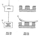
- step 31 of Fig. 3B During printing with both printing members 10 and 20 ink is first applied to the printing member (step 31 of Fig. 3B) and then transferred to the substrate 35 (Fig. 3A) as also indicated in step 33.
- PCB Printed Circuit Boards
- the present invention provides a printing or PCB member.
- the member includes a topmost protective layer, an IR ablatable layer disposed above the topmost protective layer, a substrate and a wash-off layer intermediate the topmost protective layer and the substrate.
- the wash-off layer is washed with a solvent after imagewise ablation of the topmost protective layer so as to expose the substrate, so that a printing member is produced.
- the IR ablatable layer is disposed below the topmost protective layer.
- the topmost protective layer and the IR ablatable layer are combined in one layer.
- the IR ablatable layer includes a resinous binder combined with an Infra Red absorbing dye or pigment or resins such as acrylics or polyurethanes with carbon black dispersed in resin or nigrosine dissolved in the resinous solution before deposition.
- the thickness of the IR ablatable layer is generally between 0.01 and 5 microns.
- the protective layer includes a binder resin which is insoluble in the solvent used for wash out either by its nature or by reason of the cross-linking of the resin during the deposition of the layer or a sheet of polymer or the protective layer has been derived from a cross-linkable water soluble melamine derivative plus a suitable cross-linking material such as toluene sulphonic acid, or an aqueous dispersion of polyurethane, cross-linked with a suitable cross-linking material.
- a binder resin which is insoluble in the solvent used for wash out either by its nature or by reason of the cross-linking of the resin during the deposition of the layer or a sheet of polymer or the protective layer has been derived from a cross-linkable water soluble melamine derivative plus a suitable cross-linking material such as toluene sulphonic acid, or an aqueous dispersion of polyurethane, cross-linked with a suitable cross-linking material.
- the thickness of the protective layer is generally between 0.2 and 5 microns.
- the combined layer includes a polysiloxane resin loaded with an Infra Red absorbing dye or pigment.
- the wash-off layer comprises UV curable materials and includes an alkali soluble rosin maleic resin esterified with pentaerythritol, an acrylate oligomer, a monomer-acrylate or methacrylate and a photoinitiator such as hydroxymethyl phenylpropane.
- the thickness of the wash-off layer is generally between 0.2 microns and 5 mm.
- the substrate is selected from the group of polyester, aluminum, anodized aluminum or copper cladded glass/epoxy resin.
- a printing member wherein the member is a gravure printing member and wherein the thickness of the IR ablatable layer is generally between 0.01 to 5 microns, the thickness of the protective layer is generally between 0.2 to 5 microns, the thickness of the wash-off layer is generally between 30 - 200 microns, and the thickness of the substrate is between 100 - 3,000 microns.
- Them is also provided in accordance with a preferred embodiment of the present invention a printing member wherein the member is an offset printing member and wherein the thickness of the IR ablatable layer is generally between 0.1 to 5 microns, the thickness of the protective layer is generally between 0.2 to 5 micron, the thickness of the wash-off layer is generally between 0.1 to 1 micron, and the thickness of the substrate is between 150 - 800 microns.
- a printing member wherein the member is a screen printing member, the substrate being a screen of woven polyester, cellulose fiber, nylon or stainless steel.
- a screen printing member wherein the thickness of the IR ablatable layer is generally between 0.1 to 5 microns, the thickness of the protective layer is generally between 0.2 to 5 micron, the thickness of the wash-off layer is generally between 0.1 to 5 micron, and the thickness of the substrate is between 50 - 300 micron , and wherein the wash off layer is within the material of screen or a screen printing wherein the thickness of the IR ablatable layer is generally between 0.01 to 5 microns, the thickness of the protective layer is generally between 0.2 to 5 micron and the thickness of the wash-off layer is generally between 0.1 to 5 microns.
- a printing member wherein the member is a printed circuit board member or a flexo printing member.
- the method includes the step of providing the member of the present invention, exposing it to imagwise IR radiation so as to ablate the IR absorbing layer and the protective layer and washing off the washoff layer so as to expose the substrate whereby the member ready to be used as a PCB or a printing member is ready for use.
- the step of washing further including the step of mechanically removing the wash-off layer.
- the method also includes the step of UV curing the member after said step of washing.
- the member also includes a conductive layer and the method further includes the step of etching the electrically conductive layer after the step of washing.
- the method further comprising the step of a second washing after the step of etching.
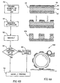
- the printing member of Fig. 4A generally referenced 40, comprises a topmost protective layer which includes an IR ablatable material, a substrate and a wash-off layer intermediate the topmost protective layer and the substrate.
- the wash-off layer is washed with a solvent after imagewise ablation of the topmost protective layer so as to expose the substrate, so that the printing member is produced ready for printing.
- printing member 40 comprises a base layer 42, a washable layer 44, a protective layer 46 and an IR ablatable layer 48.
- the base layer 42 may be any suitable substrate, such as polyester, polymide, aluminum, anodized aluminum, screen, such as a woven polyester, stainless steel or cellulose screens, or copper cladded glass/epoxy resin.
- the base layer 42 is similar to the base layer of printing members 10 and 20 (Figs. 1A and 1B) as prepared for printing.
- the washable layer 44 may be similar to the UV curable layers 4 and 24 of the prior art printing members 10 and 20, or for the PCB application it may be a washable non UV curable layer.
- the wash-off layer comprises UV curable materials and includes an alkali soluble rosin maleic resin esterified with pentaerythritol, an acrylate oligomer, a monomer-acrylate or methacrylate and a photoinitiator such as hydroxymethyl phenylpropane.
- the thickness of said wash-off layer is generally between 0.2 microns and 5 mm.
- printing member 40 also includes a protective layer 46 which protects the layer 44 during washing as described in detail hereinbelow with reference to Fig. 48.
- the protective layer 46 preferably comprises a binder resin which is insoluble in the solvent used for wash out either by its nature or by reason of the cross-linking of the resin during the deposition of the layer or a sheet of polymer.
- the protective layer may be derived from a cross-linkable water soluble melamine derivative and a suitable cross-linking material such as toluene sulphonic acid, or an aqueous dispersion of polyurethane, cross-linked with a suitable cross-linking material.
- the thickness of the protective layer is generally between 0.2 and 5 microns.
- Printing member 40 also includes an IR ablatable layer 48 which may be similar to IR ablatable layer 26 (Fig.2A).
- the protective layer 46 and the IR ablatable layer 48 may be reversed so that the protective layer 46 is uppermost and on top of the IR ablatable layer 48, or may be combined as one layer performing both functions.
- the combined layer may include a polysiloxane resin which is loaded with an Infra Red absorbing dye or pigment.
- a polysiloxane resin which is loaded with an Infra Red absorbing dye or pigment.
- the plate may be kept clean with a plastic blade covered with an absorbent material held on the surface with light pressure.
- the IR ablatable layer preferably comprises a resinous binder combined with an Infra-red absorbing dye or pigment.
- the resin may be an acrylic or a polyurethane with carbon black dispersed in the resin or nigrosine dissolved in the resinous solution before deposition.
- the thickness of the IR ablatable layer 48 is generally between 0.01 and 5 microns.
- Fig. 4B describes the method of the present invention for recording a latent image on printing member 40.
- Block 52 represents the member 40 ready for recording.
- step 54 printing member 40 is being exposed to imagewise IR laser radiation, for example to pixel by pixel digital information, which ablates both the IR ablatable layer 48 and the protective layer 46.
- a Lotem plate setter commercially available from Scitex Corporation Ltd. of Herzlia, Israel, has been used.
- step 56 the washable UV curable layer 44 is being washed by any suitable washing method, such as with water or dilute alkaline or dilute acid or solvent mixtures as known in the art.
- any suitable washing method such as with water or dilute alkaline or dilute acid or solvent mixtures as known in the art.
- dilute alkali has been used (Sodium hydroxide dissolved in water).
- mechanical cleaning can be used to assist the chemical washing or to replace it.
- the washing step of the method of the present invention precedes the UV curing step.
- the IR ablatable layer of the present invention does not have to be a UV blocking layer as in the case of the prior art recording member 20.
- member 40 may be subjected to UV curing or to printing, depending on the application for which member 40 is used.
- Printing member 40 may or may not require UV curing after washing as indicated by step 58.
- the printing member 40 may be UV cured as indicated by step 60.
- the printing member 40, now shown as printing member 40A (with or without UV curing) may be used for printing by printing apparatus 100 as indicated by step 62.
- mixture 1 represents the layer 44
- mixture 2 represent the protective layer 46
- mixture 3 represent the IR absorbing layer 48.
- the mixture was stirred until everything was dissolved to give a clear solution.
- the mixture was coated onto 175 micron polyester with a bar coater and dried in an oven for 2 minutes at 120°C. The resulting dry film was measured as 50 microns thick.
- the mixture was then bar coated on top of the previous coating to a dry coating weight of 1 gram per square meter measured after drying at 140°C for 4 minutes.
- the finished plate was then mounted on a machine as described and imaged with an Infra Red laser array as described.
- the surface of the plate was rubbed with a solution of 0.2 parts of sodium hydroxide dissolved in 31 parts of deionised water. Where there were ablated image areas, the pink first coat was removed, leaving colorless polyester film. The etch solution also removed the black surface layer but left the barrier second layer.
- the plate was then exposed to UV radiation to produce a hard gravure plate with holes corresponding to image areas.
- the plate was printed by applying gravure ink and wiping with a blade and then impressing paper onto the plate.
- the mixture was stirred until everything was dissolved to give a clear solution.
- the mixture was filtered to remove any extraneous matter and then coated onto 175 micron polyester with a Mayer rod. The coating was left to air dry for half a minute, followed by oven drying for 2 minutes at 120°C. The resulting film was measured as 40 microns thick.
- the finished plate was then mounted on a machine as described previously, and imaged with an Infra Red laser array as described.
- the surface was washed, dried and exposed to UV radiation to produce a gravure plate.
- the plate was printed by applying gravure ink and wiping it gently with a plastic blade and then impressing paper onto the plate.
- Mixture 1 was wire - rod coated onto 200 micron anodized aluminum to a dry-weight thickness of 1 gram per square centimeter and dried at 120°C for 1 minute.
- Mixtures 2 and 3 were then coated onto the surface of the coated plate exactly as described above and the resulting plate imaged and processed as previously described. After processing, the areas where the laser had affected the coating and where the coating had been subsequently cleaned off as described are left with exposed anodized aluminum which is hydrophilic and provide the back-ground of the printing plate. The Mixture 2 surface that remains is oleophilic and provides the image areas of the printing plate.
- Mixture 1 was coated onto a polythene - coated release paper to a dry weight of 30 grams per square meter. The coating was left to air dry for 1 minute and then a polyester mesh screen was laid on top of it and smoothed down with a rubber roller. The composite was then dried in the oven for 2 minutes at 120° C and then treated and imaged as described previously. The resulting product was a screen resistant to a large range of solvents after UV curing, and therefore able to be used with a large variety of inks.
- the printing member 40 is a gravure printing member
- the thickness of its IR ablatable layer is generally between 0.01 to 5 microns
- the thickness of its protective layer is generally between 0.2 to 5 microns
- the thickness of the wash-off layer is generally between 30 - 200 microns
- the thickness of the substrate is between 100 - 3,000 microns.
- the printing member 40 is an offset printing member
- the thickness of the IR ablatable layer is generally between 0.1 to 5 microns
- the thickness of said protective layer is generally between 0.2 to 5 micron
- the thickness of the wash-off layer is generally between 0.1 to 1 micron
- the thickness of said substrate is between 150 - 800 microns.
- the printing member 40 is a screen printing member, the substrate being a screen of woven polyester, cellulose fiber, nylon or stainless steel.
- the thickness of the IR ablatable layer is generally between 0.1 to 5 microns
- the thickness of the protective layer is generally between 0.2 to 5 micron
- the thickness of said wash-off layer is generally between 0.1 to 5 micron
- the thickness of the substrate is between 50 - 300 micron
- the wash off layer is within the material of screen.
- the printing member 40 is a flexo printing member.
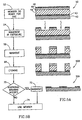
- Figs. 5A and 5B are schematic cross sectional illustration and block diagram, respectively, of a member, generally referenced 50, and a method for producing a member suitable for use as a printed circuit board according to the present invention.
- Member 50 is similar to printing member 40 except that it also includes an electrically conductive metal layer 43, an intermediate substrate 42 and a washable layer 44.
- layer 42 is laminated or coated usually with copper.
- steps 52 - 56 are similar for producing printing members 40 and 50.
- Member 50 is then etched by any etching method known in the art as indicated by step 68.
- member 50 may require additional washing (step 70) to remove the portions of washable layer 44 and the protective layer 46 which may remain on top of the copper layer. If such washing is required then these layers are being so washed (step 72).
- step 74 The resulting member 50A is now ready for use (step 74), for example as a circuit board.
- the etched member 50 is not being washed again (step 72 is omitted) and is used as is, as shown by reference numeral 50B.
- a non limiting example for producing member 50 is provided below.
- Example 2 All coating and treatment are as in Example 1 but with no UV curing, Instead, the material is soaked in a 30% Ferric Chloride.
- the above mixture was stirred and then bar coated onto an epoxy copper laminate (18 microns thick copper on 100 microns epoxy).
- the coating was dried in an oven at 140°C for 4 minute to a dried coating weight of 2 gram per square meter.
- the mixture was stirred and bar coated onto the previous mixture coating and dried in the oven at 140°C for 4 minute to a dried coating weight of 1.5 gram per square meter.
- the resulting plate was imaged and processed as described in Example 1, but with no UV curing. Instead, the material was soaked in 30% Ferric chloride at 50°C until the copper in the imaged areas was entirely etched away. The remaining coatings that had been used to protect the copper during etching were then removed by rubbing with methyl ethyl ketone.
- the finished plate was then mounted on a machine as described and imaged with an Infra Red laser array as described.
- the finished plate was then mounted on a machine as described and imaged with an Infra Red laser array as described.
- the surface of the plate was rubbed with a solution of 0.2 parts of sodium hydroxide dissolved in 31 parts of deionised water. Where there were ablated image areas, the pink first coat was removed, leaving colorless polyester film. The etch solution also removed the black surface layer but left the barrier second layer.
Landscapes
- Engineering & Computer Science (AREA)
- Manufacturing & Machinery (AREA)
- Microelectronics & Electronic Packaging (AREA)
- Physics & Mathematics (AREA)
- Optics & Photonics (AREA)
- General Physics & Mathematics (AREA)
- Printing Plates And Materials Therefor (AREA)
- Non-Metallic Protective Coatings For Printed Circuits (AREA)
Abstract

Description
| MIXTURE 1 | |
| | 15.6 parts |
| Ebecryl 1259 | 8.2 |
| Irgacure 184 | 0.48 |
| Ethyl Acetate | 15 |
| Butyl Acetate | 3 |
| Ethyl Alcohol | 15 |
| Rose Bengal | 0,09 |
| | |
| Cymel 373 | 24 |
| Deionised water | |
| 46 | |
| Cycat 4040 | 1 part |
| MIXTURE 3 | |
| Microlith Black C- | 100 |
| Isoprapanol | |
| 100 parts |
| | Rosin-maleic resin, esterified with pentaerythritol DSM Resins , 3150 AA Hoek van Holland |
| Ebecryl 1259 | Aliphatic trifunctional urethane acrylate/methacrylate diluted with 35% HPMA (Hydroxypropyl methacrylate ) UCB Chemicals, Anderlecht St. 33 - B-1620 Drogenbos - Belgium |
| Irgacure 184 | 1-hydroxy-cyclohexyl-phenyl-ketone, CIBA-Geigy, Corp., CH-4002, Basle, Switzerland. |
| Cymel 373 | methoxymethyl methylol melamine in water (85% solution) - Dyno-Cytec, Botleweg 175, 3197 KA Rotterdam, The Netherlands. |
| Cycat 4040 | Toluene sulphonic add cross-linking solution Dyno-Cytec, Botleweg 175, 3197 KA Rotterdam, The Netherlands. |
| Microlith Black C-WA | Aqueous dispersion of carbon black with acrylic resin. ClBA-Geigy, Corp., CH-4002, Basie, Switzerland. |
| MIXTURE 1 | |
| Ethyl Alcohol | 200 parts |
| Rose Bengal | 0.36 parts |
| Isopropanol | 380 parts |
| Ebecryl 1259 | 200 parts |
| Irgacure 184 | 1.7 parts |
| BYK 307 | 1 part |
| Poly Methyl vinyl ether-alt-maleic | 2 parts |
| | |
| Dehesive 410E | 135 parts |
| CAB-O-JET 200 | 45 |
| Q2-5211 | 6 |
| Cymel 373 | 21 |
| Cycat 4045 | 5.7 |
| Crosslinker V72 | 30 |
| MIXTURE 3 | |
| Deionised water | 99 parts |
| Sodium carbonate | 0.2 |
| Benzyl alcohol | 0.4 |
| Sodium dodecyl laurate | 0.2 |
| BYK 307 Poly Methyl vinyl ether-alt-maleic acid monoisopropyl ester | BYK Chemie, Wesel, Germany Aldrich Chemical Co., Milwaukee, Wisconsin, U.S.A. |
| Dehesive 410E | Wacker chemle GmbH, Munich, Germany |
| CAB-O-JET 200 | Cabot Corporation, Billerca, Massachuetts, US |
| Q2-5211 Super Wetting Agent | Dow Corporation, Midland, Ml, USA. |
| Cymel 373 | Dyno-Cytec |
| Cycat 4045 | Amine blocked P-toluene sulphonic acid, (Dyno-cytec) |
| Crosslinker V72 | Wacker |
| MIXTURE 1 | |
| Cymel 385 | 26.4 parts |
| Deionised water | 98.2 |
| Tegowet KL245 | 2.8 |
| Cycat 4040 | 1.2 |
| | |
| Cabojet 200 | 15.9 parts |
| Neorez 972 | 9.9 |
| Tegowet KL245 | 2.0 |
| Water | 9.6 |
| Isopropanol | 9.9 |
| CX-100 Crosslinker | 2.0 |
| Cymel 385 | Methoxymethyl methylol melamine-Dyno-Cytec |
| Tegowet KL245 | Tego Chemi Service GmbH, Essen, Germany |
| Neorez 972 | Zeneca Corporation, Wilmington, Massachussetts, USA |
| CX-100 Crosslinker | Zeneca |
Claims (10)
- A member comprisinga topmost protective layer;an IR ablatable layer;a substrate; anda wash-off layer for being washed with a solvent after imagewise ablation of said topmost protective layer so as to expose said substrate, so that a printing member is produced,wherein either said IR ablatable layer is disposed above topmost protective layer and said wash-off layer is intermediate said topmost protective layer and said substrate, orwherein said IR ablatable layer is disposed below said topmost protective layer and said wash-off layer is intermediate said IR ablatable layer and said substrate, orwherein said topmost protective layer and said IR ablatable layer are combined in one layer and said wash-off layer is intermediate said combined layer and said substrate.
- A member according to claim 1,wherein said IR ablatable layer comprises a resinous binder combined with an Infra Red absorbing dye or pigment; and/orwherein said IR ablatable layer comprises resins such as acrylics or polyurethanes with carbon black dispersed in resin or nigrosine dissolved in the resinous solution before deposition; and/orwherein the thickness of said IR ablatable layer is generally between 0.01 and 5 microns.
- A member according to claim 1,wherein said protective layer comprises a binder resin which is insoluble in the solvent used for wash out either by its nature or by reason of the cross-linking of the resin during the deposition of the layer or a sheet of polymer; and/or.wherein said protective layer has been derived from a cross-linkable water soluble melamine derivative plus a suitable cross-linking material such as toluene sulphonic acid, or an aqueous dispersion of polyurethane, cross-linked with a suitable cross-linking material; and/orwherein the thickness of said protective layer is generally between 0.2 and 5 microns.
- A member according to claim 1 wherein said combined layer comprises a polysiloxane resin loaded with an Infra Red absorbing dye or pigment.
- A member according to claim 1,wherein said wash-off layer comprises UV curable materials; and/orwherein said wash-off layer comprises an alkali soluble rosin maleic resin esterified with pentaerythritol, an acrylate oligomer, a monomer-acrylate or methacrylate and a photoinitiator such as hydroxymethyl phenylpropane; and/orwherein the thickness of said wash-off layer is generally between 0.2 microns and 5 mm.
- A member according to claim 1 wherein said substrate is selected from the group of polyester, aluminum, anodized aluminum, screen or copper cladded glass/epoxy resin.
- A member according to claim 1, wherein said member is any one of a group,of members including a gravure printing member, an offset printing member, a screen printing member, a printed circuit board member or a flexo printing member.
- A member according to claim 7,wherein for said gravure printing member, the thickness of said IR ablatable layer is generally between 0.01 to 5 microns, the thickness of said protective layer is generally between 0.2 to 5 microns, the thickness of said wash-off layer is generally between 30 - 200 microns, and the thickness of said substrate is between 100 - 3,000 microns, orwherein for said offset printing member, the thickness of said IR ablatable layer is generally between 0.1 to 5 microns, the thickness of said protective layer is generally between 0.2 to 5 micron, the thickness of said wash-off layer is generally between 0.1 to 1 micron, and the thickness of said substrate is between 150 - 800 microns; orwherein for screen printing member, said substrate is a screen of woven polyester, cellulose fiber, nylon or stainless steel; and/orthe thickness of said IR ablatable layer is generally between 0.1 to 5 microns, the thickness of said protective layer is generally between 0.2 to 5 micron, the thickness of said wash-off layer is generally between 0.1 to 5 micron, and the thickness of said substrate is between 50 - 300 micron , and wherein said wash off layer is within the material of screen; and/or
- , A method for producing a printing member from a provided member, said member comprising a topmost protective layer, a substrate and a wash-off layer, the method comprising the steps of:ablating said topmost protective layer by imagewise Infra Red radiation representing an image;washing off said wash-off layer so as to expose said substrate, whereby said printing member is produced.
- A method according to claim 9,wherein said step of washing further comprises the step of mechanically removing said wash-off layer; and oralso comprising the step of UV curing said member after said step of washing; and/orwherein said member also comprise a conductive layer and wherein said method further comprises the step of etching said conductive layer after said step of washing; and/orwherein said method further comprises the step of a second washing after said step of etching.
Applications Claiming Priority (2)
| Application Number | Priority Date | Filing Date | Title |
|---|---|---|---|
| IL12293098A IL122930A (en) | 1998-01-13 | 1998-01-13 | Printing and printed circuit board members and methods for producing same |
| IL12293098 | 1998-01-13 |
Publications (3)
| Publication Number | Publication Date |
|---|---|
| EP0928685A2 true EP0928685A2 (en) | 1999-07-14 |
| EP0928685A3 EP0928685A3 (en) | 1999-12-29 |
| EP0928685B1 EP0928685B1 (en) | 2004-05-12 |
Family
ID=11071085
Family Applications (1)
| Application Number | Title | Priority Date | Filing Date |
|---|---|---|---|
| EP99300262A Expired - Lifetime EP0928685B1 (en) | 1998-01-13 | 1999-01-13 | Printing and PCB members and methods for producing same |
Country Status (5)
| Country | Link |
|---|---|
| US (1) | US6352816B1 (en) |
| EP (1) | EP0928685B1 (en) |
| DE (1) | DE69917083T2 (en) |
| DK (1) | DK0928685T3 (en) |
| IL (1) | IL122930A (en) |
Cited By (6)
| Publication number | Priority date | Publication date | Assignee | Title |
|---|---|---|---|---|
| WO2001025360A1 (en) * | 1999-10-07 | 2001-04-12 | Karat Digital Press L.P. | Novel release coating |
| US6450092B2 (en) | 2000-02-01 | 2002-09-17 | Creoscitex Corporation Ltd. | Method of applying double-sided adhesive tape and gravure printing plates to gravure printing drums |
| EP1178889A4 (en) * | 1999-03-21 | 2005-10-12 | Creo Il Ltd | Gravure short run printing plate |
| WO2005103823A1 (en) * | 2004-04-23 | 2005-11-03 | Showa Denko K.K. | Photosensitive composition for black matrix |
| EP1961789A1 (en) | 2000-07-06 | 2008-08-27 | Cabot Corporation | Modified pigment products, dispersions thereof, and compositions comprising the same |
| CN116096578A (en) * | 2020-08-28 | 2023-05-09 | 柯尼卡美能达株式会社 | Ink jet head |
Families Citing this family (3)
| Publication number | Priority date | Publication date | Assignee | Title |
|---|---|---|---|---|
| RU2240922C2 (en) * | 1999-11-19 | 2004-11-27 | Кба-Жиори С.А. | Paint application plate for a rotary printing press |
| US20040241573A1 (en) * | 2003-06-02 | 2004-12-02 | Ray Kevin Barry | Thermally sensitive, white light safe mask for use in flexography |
| CN102618168A (en) * | 2012-03-14 | 2012-08-01 | 曾宪雄 | Quick-dry gravure retouching coating for gravure making and preparation method thereof |
Family Cites Families (17)
| Publication number | Priority date | Publication date | Assignee | Title |
|---|---|---|---|---|
| US5130290A (en) * | 1989-03-27 | 1992-07-14 | Kanzaki Paper Manufacturing Co., Ltd. | Water-sensitive coloring sheet |
| US5719009A (en) * | 1992-08-07 | 1998-02-17 | E. I. Du Pont De Nemours And Company | Laser ablatable photosensitive elements utilized to make flexographic printing plates |
| US5262275A (en) * | 1992-08-07 | 1993-11-16 | E. I. Du Pont De Nemours And Company | Flexographic printing element having an IR ablatable layer and process for making a flexographic printing plate |
| DE4339010C2 (en) * | 1993-06-25 | 2000-05-18 | Pt Sub Inc | Photohardenable product for printing plates |
| US5493971A (en) | 1994-04-13 | 1996-02-27 | Presstek, Inc. | Laser-imageable printing members and methods for wet lithographic printing |
| US6238837B1 (en) | 1995-05-01 | 2001-05-29 | E.I. Du Pont De Nemours And Company | Flexographic element having an infrared ablatable layer |
| US6143470A (en) | 1995-06-23 | 2000-11-07 | Nguyen; My T. | Digital laser imagable lithographic printing plates |
| DE19536805A1 (en) * | 1995-10-02 | 1997-04-03 | Basf Lacke & Farben | Multi-layer recording element suitable for the production of flexographic printing plates by digital information transmission |
| DE19536808A1 (en) * | 1995-10-02 | 1997-04-03 | Basf Lacke & Farben | Process for the production of photopolymer high pressure plates |
| DE19536806A1 (en) | 1995-10-02 | 1997-04-03 | Basf Lacke & Farben | Process for the production of photopolymer gravure plates |
| EP0864420B2 (en) * | 1997-03-11 | 2005-11-16 | Agfa-Gevaert | Heat-sensitive imaging element for making positive working printing plates |
| US5919600A (en) * | 1997-09-03 | 1999-07-06 | Kodak Polychrome Graphics, Llc | Thermal waterless lithographic printing plate |
| US6248503B1 (en) * | 1997-11-07 | 2001-06-19 | Agfa-Gevaert | Method for making positive working printing plates from a heat mode sensitive imaging element |
| AU744513B2 (en) * | 1998-01-23 | 2002-02-28 | Presstek, Inc. | Laser-imageable printing members for wet lithographic printing |
| US6120948A (en) * | 1998-03-30 | 2000-09-19 | Fuji Photo Film Co., Ltd. | Laser ablative recording material |
| US6152036A (en) * | 1998-05-28 | 2000-11-28 | Agfa-Gevaert, N.V. | Heat mode sensitive imaging element for making positive working printing plates |
| CN1205053C (en) * | 1998-09-21 | 2005-06-08 | 压缩技术公司 | Lithographic printing plates for laser imaging devices |
-
1998
- 1998-01-13 IL IL12293098A patent/IL122930A/en not_active IP Right Cessation
-
1999
- 1999-01-13 DK DK99300262T patent/DK0928685T3/en active
- 1999-01-13 DE DE69917083T patent/DE69917083T2/en not_active Expired - Fee Related
- 1999-01-13 US US09/229,706 patent/US6352816B1/en not_active Expired - Fee Related
- 1999-01-13 EP EP99300262A patent/EP0928685B1/en not_active Expired - Lifetime
Cited By (6)
| Publication number | Priority date | Publication date | Assignee | Title |
|---|---|---|---|---|
| EP1178889A4 (en) * | 1999-03-21 | 2005-10-12 | Creo Il Ltd | Gravure short run printing plate |
| WO2001025360A1 (en) * | 1999-10-07 | 2001-04-12 | Karat Digital Press L.P. | Novel release coating |
| US6450092B2 (en) | 2000-02-01 | 2002-09-17 | Creoscitex Corporation Ltd. | Method of applying double-sided adhesive tape and gravure printing plates to gravure printing drums |
| EP1961789A1 (en) | 2000-07-06 | 2008-08-27 | Cabot Corporation | Modified pigment products, dispersions thereof, and compositions comprising the same |
| WO2005103823A1 (en) * | 2004-04-23 | 2005-11-03 | Showa Denko K.K. | Photosensitive composition for black matrix |
| CN116096578A (en) * | 2020-08-28 | 2023-05-09 | 柯尼卡美能达株式会社 | Ink jet head |
Also Published As
| Publication number | Publication date |
|---|---|
| EP0928685B1 (en) | 2004-05-12 |
| IL122930A0 (en) | 1998-08-16 |
| DE69917083D1 (en) | 2004-06-17 |
| HK1019573A1 (en) | 2000-02-18 |
| IL122930A (en) | 2000-12-06 |
| EP0928685A3 (en) | 1999-12-29 |
| DE69917083T2 (en) | 2005-05-12 |
| DK0928685T3 (en) | 2004-06-28 |
| US6352816B1 (en) | 2002-03-05 |
Similar Documents
| Publication | Publication Date | Title |
|---|---|---|
| US6020108A (en) | Preparation of photopolymeric letterpress printing plates | |
| US6037102A (en) | Multilayer recording element suitable for the production of flexographic printing plates by digital information transfer | |
| US6880461B2 (en) | Method for producing flexo printing forms by means of laser-direct engraving | |
| US6245486B1 (en) | Method for imaging a printing plate having a laser ablatable mask layer | |
| US6609459B1 (en) | Gravure short run printing plate | |
| US6143470A (en) | Digital laser imagable lithographic printing plates | |
| WO2009141930A1 (en) | Flexographic printing original plate | |
| US7290487B2 (en) | Method for producing flexo printing forms by means of laser direct engraving | |
| CA2409725A1 (en) | Photosensitive resin laminate | |
| EP1417538A2 (en) | Photosensitive, flexo printing element and method for the production of newspaper flexo printing plates | |
| US6352816B1 (en) | Printing and PCB members and methods for producing same | |
| EP1194816B1 (en) | Method for producing a digitally imaged screen for use in a screen printing process | |
| WO2004051377A1 (en) | Device and method for producing flexographic plates using digital imaging, for newspaper printing | |
| EP0883835B9 (en) | Protective overcoat useful for enhancing the resistance of a printing plate precursor to ambient humidity | |
| WO1997025206A1 (en) | Methods and apparatus for preparing relief image printing plates | |
| WO2000023851A1 (en) | A printing stencil and a method for preparation thereof | |
| US6579660B1 (en) | Process for direct digital printing of circuit boards | |
| HK1019573B (en) | Printing and pcb members and methods for producing same | |
| JP4480112B2 (en) | Method for producing printing plate and screen printing plate and gravure printing plate produced using the same | |
| JP3321952B2 (en) | Offset printing method | |
| JP2007090541A (en) | Laser engraving materials and printing plate precursors for laser engraving | |
| JP2003302767A (en) | Original plate for photosensitive printing |
Legal Events
| Date | Code | Title | Description |
|---|---|---|---|
| PUAI | Public reference made under article 153(3) epc to a published international application that has entered the european phase |
Free format text: ORIGINAL CODE: 0009012 |
|
| AK | Designated contracting states |
Kind code of ref document: A2 Designated state(s): BE DE DK FR GB |
|
| AX | Request for extension of the european patent |
Free format text: AL;LT;LV;MK;RO;SI |
|
| PUAL | Search report despatched |
Free format text: ORIGINAL CODE: 0009013 |
|
| AK | Designated contracting states |
Kind code of ref document: A3 Designated state(s): AT BE CH CY DE DK ES FI FR GB GR IE IT LI LU MC NL PT SE |
|
| AX | Request for extension of the european patent |
Free format text: AL;LT;LV;MK;RO;SI |
|
| RIC1 | Information provided on ipc code assigned before grant |
Free format text: 6B 41C 1/05 A, 6H 05K 3/12 B, 6B 41C 1/10 B |
|
| 17P | Request for examination filed |
Effective date: 20000329 |
|
| AKX | Designation fees paid |
Free format text: BE DE DK FR GB |
|
| RAP1 | Party data changed (applicant data changed or rights of an application transferred) |
Owner name: CREOSCITEX CORPORATION LTD. |
|
| RAP1 | Party data changed (applicant data changed or rights of an application transferred) |
Owner name: CREO IL. LTD. |
|
| 17Q | First examination report despatched |
Effective date: 20020910 |
|
| GRAP | Despatch of communication of intention to grant a patent |
Free format text: ORIGINAL CODE: EPIDOSNIGR1 |
|
| GRAS | Grant fee paid |
Free format text: ORIGINAL CODE: EPIDOSNIGR3 |
|
| GRAA | (expected) grant |
Free format text: ORIGINAL CODE: 0009210 |
|
| AK | Designated contracting states |
Kind code of ref document: B1 Designated state(s): BE DE DK FR GB |
|
| REG | Reference to a national code |
Ref country code: GB Ref legal event code: FG4D |
|
| REF | Corresponds to: |
Ref document number: 69917083 Country of ref document: DE Date of ref document: 20040617 Kind code of ref document: P |
|
| REG | Reference to a national code |
Ref country code: DK Ref legal event code: T3 |
|
| REG | Reference to a national code |
Ref country code: HK Ref legal event code: GR Ref document number: 1019573 Country of ref document: HK |
|
| ET | Fr: translation filed | ||
| PLBE | No opposition filed within time limit |
Free format text: ORIGINAL CODE: 0009261 |
|
| STAA | Information on the status of an ep patent application or granted ep patent |
Free format text: STATUS: NO OPPOSITION FILED WITHIN TIME LIMIT |
|
| 26N | No opposition filed |
Effective date: 20050215 |
|
| PGFP | Annual fee paid to national office [announced via postgrant information from national office to epo] |
Ref country code: DE Payment date: 20060112 Year of fee payment: 8 |
|
| PGFP | Annual fee paid to national office [announced via postgrant information from national office to epo] |
Ref country code: FR Payment date: 20060113 Year of fee payment: 8 Ref country code: DK Payment date: 20060113 Year of fee payment: 8 |
|
| PGFP | Annual fee paid to national office [announced via postgrant information from national office to epo] |
Ref country code: BE Payment date: 20060207 Year of fee payment: 8 |
|
| PG25 | Lapsed in a contracting state [announced via postgrant information from national office to epo] |
Ref country code: DE Free format text: LAPSE BECAUSE OF NON-PAYMENT OF DUE FEES Effective date: 20070801 |
|
| GBPC | Gb: european patent ceased through non-payment of renewal fee |
Effective date: 20070113 |
|
| REG | Reference to a national code |
Ref country code: DK Ref legal event code: EBP |
|
| REG | Reference to a national code |
Ref country code: FR Ref legal event code: ST Effective date: 20070930 |
|
| PG25 | Lapsed in a contracting state [announced via postgrant information from national office to epo] |
Ref country code: GB Free format text: LAPSE BECAUSE OF NON-PAYMENT OF DUE FEES Effective date: 20070113 |
|
| BERE | Be: lapsed |
Owner name: *CREO IL. LTD Effective date: 20070131 |
|
| PG25 | Lapsed in a contracting state [announced via postgrant information from national office to epo] |
Ref country code: BE Free format text: LAPSE BECAUSE OF NON-PAYMENT OF DUE FEES Effective date: 20070131 |
|
| PG25 | Lapsed in a contracting state [announced via postgrant information from national office to epo] |
Ref country code: DK Free format text: LAPSE BECAUSE OF NON-PAYMENT OF DUE FEES Effective date: 20070131 |
|
| PG25 | Lapsed in a contracting state [announced via postgrant information from national office to epo] |
Ref country code: FR Free format text: LAPSE BECAUSE OF NON-PAYMENT OF DUE FEES Effective date: 20070131 |
|
| PGFP | Annual fee paid to national office [announced via postgrant information from national office to epo] |
Ref country code: GB Payment date: 20060120 Year of fee payment: 8 |