EP0928049A2 - Stacked lan connector - Google Patents
Stacked lan connector Download PDFInfo
- Publication number
- EP0928049A2 EP0928049A2 EP98310795A EP98310795A EP0928049A2 EP 0928049 A2 EP0928049 A2 EP 0928049A2 EP 98310795 A EP98310795 A EP 98310795A EP 98310795 A EP98310795 A EP 98310795A EP 0928049 A2 EP0928049 A2 EP 0928049A2
- Authority
- EP
- European Patent Office
- Prior art keywords
- connector
- board
- serial bus
- cavity
- contacts
- Prior art date
- Legal status (The legal status is an assumption and is not a legal conclusion. Google has not performed a legal analysis and makes no representation as to the accuracy of the status listed.)
- Granted
Links
Images


Classifications
-
- H—ELECTRICITY
- H01—ELECTRIC ELEMENTS
- H01R—ELECTRICALLY-CONDUCTIVE CONNECTIONS; STRUCTURAL ASSOCIATIONS OF A PLURALITY OF MUTUALLY-INSULATED ELECTRICAL CONNECTING ELEMENTS; COUPLING DEVICES; CURRENT COLLECTORS
- H01R27/00—Coupling parts adapted for co-operation with two or more dissimilar counterparts
- H01R27/02—Coupling parts adapted for co-operation with two or more dissimilar counterparts for simultaneous co-operation with two or more dissimilar counterparts
-
- H—ELECTRICITY
- H01—ELECTRIC ELEMENTS
- H01R—ELECTRICALLY-CONDUCTIVE CONNECTIONS; STRUCTURAL ASSOCIATIONS OF A PLURALITY OF MUTUALLY-INSULATED ELECTRICAL CONNECTING ELEMENTS; COUPLING DEVICES; CURRENT COLLECTORS
- H01R12/00—Structural associations of a plurality of mutually-insulated electrical connecting elements, specially adapted for printed circuits, e.g. printed circuit boards [PCB], flat or ribbon cables, or like generally planar structures, e.g. terminal strips, terminal blocks; Coupling devices specially adapted for printed circuits, flat or ribbon cables, or like generally planar structures; Terminals specially adapted for contact with, or insertion into, printed circuits, flat or ribbon cables, or like generally planar structures
- H01R12/70—Coupling devices
- H01R12/71—Coupling devices for rigid printing circuits or like structures
- H01R12/712—Coupling devices for rigid printing circuits or like structures co-operating with the surface of the printed circuit or with a coupling device exclusively provided on the surface of the printed circuit
- H01R12/716—Coupling device provided on the PCB
-
- H—ELECTRICITY
- H01—ELECTRIC ELEMENTS
- H01R—ELECTRICALLY-CONDUCTIVE CONNECTIONS; STRUCTURAL ASSOCIATIONS OF A PLURALITY OF MUTUALLY-INSULATED ELECTRICAL CONNECTING ELEMENTS; COUPLING DEVICES; CURRENT COLLECTORS
- H01R13/00—Details of coupling devices of the kinds covered by groups H01R12/70 or H01R24/00 - H01R33/00
- H01R13/64—Means for preventing incorrect coupling
- H01R13/641—Means for preventing incorrect coupling by indicating incorrect coupling; by indicating correct or full engagement
-
- H—ELECTRICITY
- H01—ELECTRIC ELEMENTS
- H01R—ELECTRICALLY-CONDUCTIVE CONNECTIONS; STRUCTURAL ASSOCIATIONS OF A PLURALITY OF MUTUALLY-INSULATED ELECTRICAL CONNECTING ELEMENTS; COUPLING DEVICES; CURRENT COLLECTORS
- H01R13/00—Details of coupling devices of the kinds covered by groups H01R12/70 or H01R24/00 - H01R33/00
- H01R13/648—Protective earth or shield arrangements on coupling devices, e.g. anti-static shielding
- H01R13/658—High frequency shielding arrangements, e.g. against EMI [Electro-Magnetic Interference] or EMP [Electro-Magnetic Pulse]
- H01R13/6581—Shield structure
- H01R13/659—Shield structure with plural ports for distinct connectors
-
- H—ELECTRICITY
- H01—ELECTRIC ELEMENTS
- H01R—ELECTRICALLY-CONDUCTIVE CONNECTIONS; STRUCTURAL ASSOCIATIONS OF A PLURALITY OF MUTUALLY-INSULATED ELECTRICAL CONNECTING ELEMENTS; COUPLING DEVICES; CURRENT COLLECTORS
- H01R13/00—Details of coupling devices of the kinds covered by groups H01R12/70 or H01R24/00 - H01R33/00
- H01R13/648—Protective earth or shield arrangements on coupling devices, e.g. anti-static shielding
- H01R13/658—High frequency shielding arrangements, e.g. against EMI [Electro-Magnetic Interference] or EMP [Electro-Magnetic Pulse]
- H01R13/6591—Specific features or arrangements of connection of shield to conductive members
- H01R13/6594—Specific features or arrangements of connection of shield to conductive members the shield being mounted on a PCB and connected to conductive members
-
- H—ELECTRICITY
- H01—ELECTRIC ELEMENTS
- H01R—ELECTRICALLY-CONDUCTIVE CONNECTIONS; STRUCTURAL ASSOCIATIONS OF A PLURALITY OF MUTUALLY-INSULATED ELECTRICAL CONNECTING ELEMENTS; COUPLING DEVICES; CURRENT COLLECTORS
- H01R13/00—Details of coupling devices of the kinds covered by groups H01R12/70 or H01R24/00 - H01R33/00
- H01R13/66—Structural association with built-in electrical component
- H01R13/717—Structural association with built-in electrical component with built-in light source
- H01R13/7175—Light emitting diodes (LEDs)
-
- H—ELECTRICITY
- H01—ELECTRIC ELEMENTS
- H01R—ELECTRICALLY-CONDUCTIVE CONNECTIONS; STRUCTURAL ASSOCIATIONS OF A PLURALITY OF MUTUALLY-INSULATED ELECTRICAL CONNECTING ELEMENTS; COUPLING DEVICES; CURRENT COLLECTORS
- H01R2201/00—Connectors or connections adapted for particular applications
- H01R2201/04—Connectors or connections adapted for particular applications for network, e.g. LAN connectors
-
- H—ELECTRICITY
- H01—ELECTRIC ELEMENTS
- H01R—ELECTRICALLY-CONDUCTIVE CONNECTIONS; STRUCTURAL ASSOCIATIONS OF A PLURALITY OF MUTUALLY-INSULATED ELECTRICAL CONNECTING ELEMENTS; COUPLING DEVICES; CURRENT COLLECTORS
- H01R24/00—Two-part coupling devices, or either of their cooperating parts, characterised by their overall structure
- H01R24/60—Contacts spaced along planar side wall transverse to longitudinal axis of engagement
- H01R24/62—Sliding engagements with one side only, e.g. modular jack coupling devices
-
- H—ELECTRICITY
- H01—ELECTRIC ELEMENTS
- H01R—ELECTRICALLY-CONDUCTIVE CONNECTIONS; STRUCTURAL ASSOCIATIONS OF A PLURALITY OF MUTUALLY-INSULATED ELECTRICAL CONNECTING ELEMENTS; COUPLING DEVICES; CURRENT COLLECTORS
- H01R25/00—Coupling parts adapted for simultaneous co-operation with two or more identical counterparts, e.g. for distributing energy to two or more circuits
- H01R25/006—Coupling parts adapted for simultaneous co-operation with two or more identical counterparts, e.g. for distributing energy to two or more circuits the coupling part being secured to apparatus or structure, e.g. duplex wall receptacle
-
- Y—GENERAL TAGGING OF NEW TECHNOLOGICAL DEVELOPMENTS; GENERAL TAGGING OF CROSS-SECTIONAL TECHNOLOGIES SPANNING OVER SEVERAL SECTIONS OF THE IPC; TECHNICAL SUBJECTS COVERED BY FORMER USPC CROSS-REFERENCE ART COLLECTIONS [XRACs] AND DIGESTS
- Y10—TECHNICAL SUBJECTS COVERED BY FORMER USPC
- Y10T—TECHNICAL SUBJECTS COVERED BY FORMER US CLASSIFICATION
- Y10T29/00—Metal working
- Y10T29/49—Method of mechanical manufacture
- Y10T29/49002—Electrical device making
- Y10T29/49117—Conductor or circuit manufacturing
- Y10T29/49124—On flat or curved insulated base, e.g., printed circuit, etc.
- Y10T29/4913—Assembling to base an electrical component, e.g., capacitor, etc.
- Y10T29/49133—Assembling to base an electrical component, e.g., capacitor, etc. with component orienting
- Y10T29/49137—Different components
-
- Y—GENERAL TAGGING OF NEW TECHNOLOGICAL DEVELOPMENTS; GENERAL TAGGING OF CROSS-SECTIONAL TECHNOLOGIES SPANNING OVER SEVERAL SECTIONS OF THE IPC; TECHNICAL SUBJECTS COVERED BY FORMER USPC CROSS-REFERENCE ART COLLECTIONS [XRACs] AND DIGESTS
- Y10—TECHNICAL SUBJECTS COVERED BY FORMER USPC
- Y10T—TECHNICAL SUBJECTS COVERED BY FORMER US CLASSIFICATION
- Y10T29/00—Metal working
- Y10T29/49—Method of mechanical manufacture
- Y10T29/49002—Electrical device making
- Y10T29/49117—Conductor or circuit manufacturing
- Y10T29/49124—On flat or curved insulated base, e.g., printed circuit, etc.
- Y10T29/49147—Assembling terminal to base
Definitions
- This invention relates to the field of electrical connectors and, more particularly, to connectors mountable onto circuit boards.
- Electronic apparatus such as a computer, is required to provide connectors at input/output ports that accommodate mating with a plurality of external cables, with the internal connectors conventionally mounted onto a circuit board.
- One such connector is disclosed in PCT Patent Publication No WO97/10628 to be a shielded serial bus receptacle connector providing a pair of plug-receiving cavities for mating with two serial bus plug connectors simultaneously, for a Local Area Network (LAN).
- LAN Local Area Network
- the computer provides at the I/O port a modular jack connector matable with modular plug connectors of a design standard in telephony.
- US Patent Nos 4 978 317 and 5 685 737 to provide modular jacks with LEDs along the observable mating face at the I/O port as visual indicators of full mating with a plug connector with the modular jack.
- the present invention provides a LAN connector having a pair of plug-receiving cavities stacked beneath a modular jack, so that the connector assembly is matable with a modular plug and two serial bus plug connectors simultaneously, while occupying only incrementally more circuit board real estate than would be taken up by a stacked serial bus receptacle.
- the assembly also provides a pair of LEDs at the mating face that visually indicate at the I/O port whether or not a modular plug is fully mated. Shielding is provided surrounding the assembly above the circuit board and also between the modular jack and its contacts and the serial bus receptacle and its contacts.
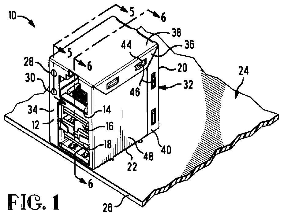
- Stacked LAN connector 10 of the present invention is seen in FIG 1 having a mating face 12 providing a modular plug-receiving cavity 14 and two USB plug receiving cavities 16,18 extending rearwardly toward rear face 20.
- Connector 10 includes a board-mounting face 22, orthogonal to both mating face 12 and rear face 20, for mounting to circuit board 24 along an edge 26 thereof.
- two light-emitting devices (LEDs) 28,30 beside modular plug-receiving cavity 14 for visually indicating full mating of a modular plug connector (not shown) thereinto.
- An outer shield 32 is seen enveloping connector assembly 10 and having a front wall 34 along mating face 12, and is appropriately apertured to expose modular plug-receiving cavity 14 and USB plug-receiving cavities 16,18 and also the lenses of LEDs 28,30.
- Flaps 36 of top shield wall 38 and flaps 40 of rear shield wall 42 include slots 44 that lock over embossments 46 of side shield walls 48, to secure thereto as the top and rear walls are bent around the main housing and the flaps are bent to coextend along side walls 48 at the completion of connector assembly.
- FIGS. 2 and 3 In FIGS. 2 and 3 is seen main housing 50 of insulative material, USB component 150, modular jack component 200, LEDs 28,30 and contacts 52 associated with respective ones of leads 54 of LEDs 28,30 for electrically interconnecting them by way of posts 56 to appropriate circuits of circuit board 24 at through holes 58.
- Outer shield 32 includes ground legs 60 insertable into respective through holes 62 of circuit board 24 for grounding.
- Outer shield 32 is shown in FIGS. 2 and 3 as being generally cubic in shape, although the shape shown is only achieved after the walls of the outer shield have been folded to envelope the assembly of the main housing and the LED, modular jack and stacked USB components therewithin, as described hereinbelow.
- Main housing 50 (FIGS. 2 to 4) provides a first or USB component-receiving cavity 64 extending rearwardly thereinto from front face 66 for receipt thereinto of USB component 150; the main housing further includes a pair of LED-receiving apertures 68 for LEDs 28,30 extending rearwardly from front face 66, and a modular jack-receiving cavity 70 extending into rear face 72 for receipt thereinto of modular jack component 200.
- Main housing 50 also is seen to define a second or modular plug-receiving cavity 14 associated with modular jack component 200 and extending rearwardly to communicate with modular jack-receiving cavity 70, and to define a latching section 74 along top wall 76 in communication with plug-receiving cavity 14 for latching thereinto of a latch arm of a modular plug connector (not shown) during mating.
- Main housing 50 is seen in FIGS. 4 and 5 to include a contact-receiving aperture 78 extending upwardly from bottom face 80, with pairs of opposed slots 82 adapted to receive LED contacts 52 therealong.
- IDC slots 84 at upper ends of contacts 52 are received compressively around leads 54 to establish an electrical connection therewith.
- Pairs of opposed barbs 86 at lower ends of the contacts form an interference fit in slots 82 for retention of the contacts in main housing 50 after full insertion thereinto.
- the lenses of LEDs 28,30 extend forwardly through holes 88 in front shield wall 34, as seen in FIG. 5.
- modular jack-receiving cavity 70 of main housing 50 includes insert-receiving opening 90 extending forwardly from the upper portion of cavity 70 and is in communication with modular plug-receiving cavity 14 (FIG. 2).
- Stacked USB component 150 is shown in FIG. 7 to include an outer shield 152, an insulative housing 154, an inner shield 156 and a plurality of contacts 158.
- Partition 160 of housing 154 establishes a pair of plug-receiving cavities 162,164, and contacts 158 include contact sections 166 disposed along support walls 168 opposing partition 160 thereby being exposed in plug-receiving cavities 162,164 for electrical connection with contacts of the USB plug connectors (not shown).
- Contacts 158 further include board-connecting posts 170 that extend downwardly beyond board-mounting face 172 for electrical engagement with circuits of circuit board 24 at through holes 174 upon board mounting.
- stacked USB component 150 includes inner shield 156 that includes spring arms 176 that extend along partition 160 to engage the shield of a mating USB plug connector along one side, while spring arms 178 of outer shield 152 engage the plug's shield along the opposite side for assured grounding. Additional spring arms 180 along side walls 182 of outer shield 152 engage webs 184 of inner shield 156 for grounding interconnection therewith, and outer shield 152 includes ground legs 186 depending beneath board-mounting face 172 for initial board retention and for electrical connection to a ground circuits of board 24 at holes 188.
- outer shield 152 includes a pair of panel-engaging fingers 190 that extend toward each other forwardly of partition 160 to groundingly engage the panel portion extending horizontally between a pair of cutouts that provide for insertion of the USB plug connectors through the panel for connector mating.
- Rear shield 130 is provided that is secured to outer shield 152 of USB component 150 along the rearward end thereof.
- Rear shield 130 has a rear plate 132, a window 134 through the top end of rear plate, and a top wall section 136 extending forwardly from the top edge of rear plate 132.
- Locking sections 138 extend forwardly from side edges of rear plate 132 that extend along inner surfaces of side walls 182 of outer shield 152 and are initially deflected inwardly toward each other during assembly, and locking sections 138 include pairs of locking tabs 140 extending outwardly to define a U-shape aligned with spring arms 180 and that seat in cutouts 192 in outer shield side walls 182, above and below spring arms 180, to lock the rear shield along the rearward end of USB component 150.
- Stacked USB component 150 is mounted in main housing 50 as indicated in FIG. 6.
- Main housing 50 includes a projection 92 extending forwardly into plug-receiving cavity 14 to define a slot 94 thereabove.
- Projection 92 is received through window 134 of rear shield 130, and slot 94 receives thereinto rear portion 194 of the upper wall of outer shield 152 and top wall section 136, establishing fixing of upper rear portion of USB component 150 against movement in the vertical direction; side walls of cavity 64 restrain its movement in the side-to-side direction; and the inner surface of front wall 34 of outer shield 32 is abutted by the outturned flanges 196 of the front wall of outer shield 152 of the USB component surrounding the apertures aligned with the plug-receiving openings 16,18.
- Bottom flange 96 extends rearwardly from the bottom edge of front shield wall 34 to retain the lower front portion of USB component 150 in the connector assembly.
- modular jack component 200 includes a first housing 202, second housing or insert 204 and a plurality of contacts 206, with the first and second housings insert molded about portions of the body sections of the contacts.
- FIG. 8 is merely illustrative of the portions of component 200, since housings 202,204 do not exist as discrete members separate from the contacts in the preferred embodiment but are insert molded about the contacts.
- the contacts are initially stamped in carrier strip form, with both ends of each of the contacts initially joined to opposed carrier strips 208,210.
- Modular jack component 200 is similar to the connector disclosed in U.S. Patent No. 5,362,257.
- Contacts 206 include board-connecting posts 212 at first ends of body sections 214 that will depend beneath board-mounting face 22 for insertion into board through-holes 216 for connection to circuits of circuit board 24 (FIG. 2). At the opposed ends, contact sections 218 will be angled rearwardly from front nose 220 of insert 204 and disposed in modular plug-receiving cavity 14 upon complete assembly of stacked LAN connector 10 (see FIG. 6).
- first and second housings 202,204 have been molded around respective first and second portions 222,224 of body sections 214 (prior to forming right angle bends 226 between the respective body section portions), so first and second housings 202,204 are initially generally coplanar, and carrier strips 208,210 have been severed from both ends of all contacts 206. Thereafter, the body sections of the contacts are bent into a right angle at bends 226 such that first housing 202 is oriented orthogonally to second housing 204 as is seen in FIG. 10.
- Rearward end portion 228 of second housing 204 defines a rear face 230 that bears against rounded ribs 232 (FIG. 8) along top face 234 of first housing 202 during bending of the molded subassembly, whereafter latching projections 236 along side surfaces 238 enter recesses 240 to latch beneath arms 242 along sides of top face 234 to secure the second housing 204 in position at right angles to first housing 202, as seen in FIG. 10.
- Second housing 204 includes a forward section 244 extending to a front end or nose 220, around which contacts 206 are bent to extend backwardly with contact sections 218 angled upwardly, as seen in FIG. 10.
- Forward section 244 of second housing 204 includes guide rails 246 that are inserted into main housing 50 and into guide slots 98 (FIG. 4) along side surfaces of opening 90 forwardly of jack-receiving cavity 70, when modular jack component 200 is inserted into main housing 40.
- Upstanding bosses 248 along sides of rearward section 228 include lateral flanges 250 that enter corresponding slots 100 above guide slots 98.
- First housing 202 now vertically oriented, includes guide rails 252 adjacent the bottom end thereof, that enter guide slots 102 along sides of cavity 70.
- Latch surfaces 254 are defined by embossments 256 along side surfaces of first housing 202 at forward ends of guide rails 252, that seat forwardly of latching ledges 104 also defined along sides of cavity 70 above guide slots 102, securing modular jack component 200 in position in main housing 50.
- stacked LAN connector 10 preferably LEDs 28,30 and LED contacts 52 are assembled into main housing 50, then modular jack component 200 is assembled into main housing 50, after which stacked USB component 150 is inserted, all as seen in FIGS. 11 to 14.
- contact sections 218 pass through vertical slots 106 in transverse partition wall 108 (FIGS. 13 and 14) that also secure the free ends of contact sections 218 precisely in position biased against the upper ends of the slots to assure the desired angle when unmated, while allowing vertical movement as the contact sections are deflected downwardly by mating contacts upon insertion of a modular plug connector into cavity 14 during mating.
- outer shield 32 is folded to envelope main housing 50 and secure stacked USB component 150 in position along mating face 12, by first positioning front wall 34 along front face 66 of main housing 50 with lenses of LEDs 28,30 protruding through corresponding holes 88.
- Bottom flange 96 of front wall 34 extends or is folded rearwardly against the front portion of the main housing along board mounting face 22, to lie beneath the front portion of stacked USB component 150 to cooperate in assuring the fixing of stacked USB component 150 against vertical movement, as seen in FIG. 6.
- Side walls 48 and top wall 38 extend or are folded rearwardly along housing sides 110 and top surface 76 respectively, whereafter rear wall 42 is folded down from the rear edge of top shield wall 38 to be disposed along rear face 72 of main housing 50. Flaps 36,40 are then folded along side shield walls 48 with embossments 46 locking in slots 44.
- a conventional stacked USB connector is accommodated without modification in the stacked LAN connector.
- a shield member is secured to the rearward end of the USB connector without modification thereto, for shielding between the USB component contacts and the modular jack contacts.
- Substantial savings in circuit board real estate result in placing the modular jack component above the stacked USB connector, so that the connector accommodates either LAN or peripheral connections or both simultaneously, while internal and external shielding of the contacts of both the modular jack and stacked USB components assures the integrity of the signals transmitted from mating connectors to the circuits of the circuit board.
- Convenience results from providing an assembly that is manipulatable as a unit for board placement, such as by pick-and-place equipment prior to soldering of the contacts and shield ground sections to the circuits of the circuit board.
Landscapes
- Details Of Connecting Devices For Male And Female Coupling (AREA)
- Coupling Device And Connection With Printed Circuit (AREA)
- Connector Housings Or Holding Contact Members (AREA)
Abstract
Description
Claims (9)
- A stacked LAN electrical connector (10) comprisingan insulative housing (50) having a first cavity (64), a second cavity (14), a mating face (66) and a board-mounting face (22);a serial bus connector (150) disposed in said first cavity (64) and including at least one plug-receiving cavity (16,18) in communication with the mating face (66) of the housing and a first array of board-connectable contacts (158) having contact sections (166) exposed in the plug-receiving cavity;a modular jack connector (200) stacked with respect to the serial bus connector (150) and including a second array of board-connectable contacts (206) disposed in the insulative housing (50) and having contact sections (218) exposed in the second cavity (14) in communication with the mating face (66) of the housing;board-connecting contact sections (170;222) of the first and second arrays of contacts (158,206) extending at least to the board-mounting face (22) of the insulative housing (50); anda shield (130) in the insulative housing (50) between the board-connecting contact sections (170:222) of the first and second arrays of contacts (158,206).
- The connector of claim 1, wherein the modular jack connector (200) is positioned above the serial bus connector (150).
- The connector of claim 1 or 2, wherein the serial bus connector (150) is a stacked serial bus connector having two plug-receiving cavities (16,18) and is insertable into the first aperture (64) of the insulative housing from the mating face (66).
- The connector of claim 1, 2 or 3, wherein the modular jack connector includes a modular jack component (200) insertable into the insulative housing (50) from rearwardly thereof and including a portion (202) substantially orthogonal to said board mounting face (22) and disposed rearwardly of the serial bus connector (150) and containing portions (222) of the second array of contacts (206) that are substantially orthogonal to said board mounting face, said modular jack component including guide rails (246,250,252) following guide slots (98,100,102) of the insulative housing (50) for accurate positioning, and latching into position so that the contact sections (218) of the second array of contacts (206) are exposed in said second cavity (14).
- The connector of any preceding claim, wherein the insulative housing (50) includes a pair of LEDs (28,30) secured therein, each LED including a light-emitting lens exposed along the mating face (66) and board-connecting sections (52,56) extending at least to the board-mounting face (22) of the insulative housing.
- The connector of any preceding claim, wherein the shield (130) between the board-connecting sections (170;222) of the first and second arrays of contacts (158;206) is a rear shield (130) affixed along a rear face of the serial bus connector (150) rearwardly of board-connecting sections (170) of said first array of contacts (158), electrically connected with an outer shield (152) of the serial bus connector (150), said rear shield (130) includes a window (134) along a rear plate (132) thereof, and a projection (92) extends forwardly into said first cavity (64) from a rear wall thereof and through said window (134) upon insertion of the serial bus connector (150) into the first cavity (64) to assist in retention of the stacked serial bus connector in said first cavity.
- The connector of any preceding claim, wherein an outer shield (32) is affixed around the insulative housing (50) to shield both the serial bus connector (150) and the modular jack connector (200).
- The connector of claim 7, wherein flaps (36) of a top wall (38) of said outer shield (32) and flaps (40) of a rear wall (42) of said outer shield include slots (44) that lock over embossments 46) of side walls (48) of the outer shield when said flaps (36,40) are folded to coextend along portions of said side walls adjacent thereto, upon assembly of the outer shield around the insulative housing (50), to secure said outer shield around the insulative housing.
- The connector of claim 7 or 8, wherein the outer shield (32) includes a front wall (34) surrounding the first and second cavities (64,14), and a portion of an outer shield (152) of the serial bus connector (150) abuts portions of said front wall (34) of said outer shield (32) adjacent said first cavity (64) to assist in retention of the serial bus connector (150) in said first cavity (64)
Applications Claiming Priority (2)
| Application Number | Priority Date | Filing Date | Title |
|---|---|---|---|
| US7003197P | 1997-12-30 | 1997-12-30 | |
| US70031P | 1997-12-30 |
Publications (3)
| Publication Number | Publication Date |
|---|---|
| EP0928049A2 true EP0928049A2 (en) | 1999-07-07 |
| EP0928049A3 EP0928049A3 (en) | 2000-12-27 |
| EP0928049B1 EP0928049B1 (en) | 2004-04-21 |
Family
ID=22092704
Family Applications (1)
| Application Number | Title | Priority Date | Filing Date |
|---|---|---|---|
| EP98310795A Expired - Lifetime EP0928049B1 (en) | 1997-12-30 | 1998-12-30 | Stacked lan connector |
Country Status (6)
| Country | Link |
|---|---|
| US (1) | US6162089A (en) |
| EP (1) | EP0928049B1 (en) |
| JP (1) | JP4070166B2 (en) |
| CN (1) | CN1153113C (en) |
| DE (1) | DE69823323T2 (en) |
| TW (1) | TW417850U (en) |
Cited By (9)
| Publication number | Priority date | Publication date | Assignee | Title |
|---|---|---|---|---|
| EP1089396A3 (en) * | 1999-09-29 | 2001-11-28 | Molex Incorporated | Reduced-size connector |
| EP1122839A3 (en) * | 2000-02-02 | 2003-05-14 | J.S.T MFG Co. Ltd. | Modular jack |
| EP1096757A3 (en) * | 1999-10-26 | 2003-09-03 | Matsushita Electric Industrial Co., Ltd. | Earphone jack holding device |
| EP1278271A3 (en) * | 2001-07-18 | 2003-09-17 | J.S.T. Mfg. Co., Ltd. | Assembly of electric connectors |
| WO2007062144A1 (en) | 2005-11-23 | 2007-05-31 | Draeger Medical Systems, Inc. | A connector system |
| US7249977B2 (en) | 2002-08-16 | 2007-07-31 | Harting Electric Gmbh & Co. Kg | USB type plug connector |
| WO2013063233A1 (en) * | 2011-10-28 | 2013-05-02 | 3M Innovative Properties Company | Electrical connector |
| EP2728486A3 (en) * | 2012-10-23 | 2014-07-02 | Google, Inc. | Ethernet connector with integrated USB |
| US9484680B2 (en) | 2013-06-12 | 2016-11-01 | Intel Corporation | Radio frequency interference shield |
Families Citing this family (118)
| Publication number | Priority date | Publication date | Assignee | Title |
|---|---|---|---|---|
| US6310781B1 (en) * | 1999-03-31 | 2001-10-30 | Cisco Technology, Inc. | Connection pin layout for connecting integrated magnetics modules to a printed circuit board |
| US7438598B1 (en) | 1999-11-05 | 2008-10-21 | Yamaichi Electronics Co., Ltd. | Card connector |
| JP3396457B2 (en) * | 2000-02-08 | 2003-04-14 | 山一電機株式会社 | Card connector |
| JP2001313128A (en) | 2000-04-27 | 2001-11-09 | Yamaichi Electronics Co Ltd | Card connector |
| JP3530460B2 (en) | 2000-04-27 | 2004-05-24 | 山一電機株式会社 | Card connector |
| US20020090859A1 (en) * | 2000-05-26 | 2002-07-11 | Richard Brayden | Vertically integrated card housing |
| US6541878B1 (en) | 2000-07-19 | 2003-04-01 | Cisco Technology, Inc. | Integrated RJ-45 magnetics with phantom power provision |
| JP3825614B2 (en) | 2000-08-08 | 2006-09-27 | 山一電機株式会社 | Card edge connector |
| US6439922B1 (en) * | 2000-09-20 | 2002-08-27 | Tyco Electronics Corporation | Visual indicators having common cathode leads, and an electrical connector using same |
| TW460050U (en) * | 2000-10-20 | 2001-10-11 | Hon Hai Prec Ind Co Ltd | Electrical connector assembly |
| JP3544521B2 (en) * | 2000-11-28 | 2004-07-21 | 日本圧着端子製造株式会社 | Modular jack |
| TW483535U (en) * | 2000-12-01 | 2002-04-11 | Jess Link Products Co Ltd | Slot device capable of being inserted with various cards for handheld computer |
| US6585540B2 (en) * | 2000-12-06 | 2003-07-01 | Pulse Engineering | Shielded microelectronic connector assembly and method of manufacturing |
| US6368151B1 (en) * | 2000-12-29 | 2002-04-09 | Cheng Uei Precision Industry Co., Ltd. | Electrical connector assembly |
| JP4181307B2 (en) | 2001-01-19 | 2008-11-12 | 山一電機株式会社 | Card connector |
| JP2002237340A (en) | 2001-02-09 | 2002-08-23 | Yamaichi Electronics Co Ltd | Card edge connector |
| JP3464461B2 (en) * | 2001-03-07 | 2003-11-10 | 山一電機株式会社 | Contact terminal and card connector including the same |
| US20020146940A1 (en) * | 2001-04-10 | 2002-10-10 | Robert Colantuono | Magnetically integrated jack |
| US6835091B2 (en) * | 2001-07-06 | 2004-12-28 | Fci Americas Technology, Inc. | Universal serial bus electrical connector |
| TW516739U (en) * | 2001-09-20 | 2003-01-01 | Tekcon Electronics Corp | Stacked connector assembly |
| US6474999B1 (en) * | 2001-11-01 | 2002-11-05 | Hon Hai Precision Ind. Co., Ltd. | Electrical connector having printed circuit board mounted therein |
| TW510607U (en) * | 2001-11-15 | 2002-11-11 | Hon Hai Prec Ind Co Ltd | Electrical connector assembly |
| US20030157843A1 (en) * | 2002-02-15 | 2003-08-21 | Keith Thomas | Stacking connector with improper plug type prevention |
| US6773298B2 (en) | 2002-05-06 | 2004-08-10 | Pulse Engineering, Inc. | Connector assembly with light source sub-assemblies and method of manufacturing |
| USD468267S1 (en) | 2002-05-30 | 2003-01-07 | Hon Hai Precision Ind. Co., Ltd. | Electrical connector assembly |
| USD468695S1 (en) | 2002-06-06 | 2003-01-14 | Hon Hai Precision Ind. Co., Ltd. | Electrical connector assembly |
| USD473193S1 (en) | 2002-08-16 | 2003-04-15 | Hon Hai Precision Ind. Co., Ltd. | Electrical connector assembly |
| US6688914B1 (en) | 2002-09-06 | 2004-02-10 | Hon Hai Precision Ind. Co., Ltd. | Stacked electrical connector assembly having easily detachable electronic module |
| US6688909B1 (en) | 2002-10-03 | 2004-02-10 | Hon Hai Precision Ind. Co., Ltd. | Stacked connector with leds |
| US6638121B1 (en) | 2002-10-04 | 2003-10-28 | Hon Hai Precision Ind. Co., Ltd. | Stacked connector with LEDs and method of producing the same |
| US6682365B1 (en) | 2002-11-05 | 2004-01-27 | Hon Hai Precision Ind. Co., Ltd. | Stacked connector with plastic part assembled thereto |
| US6964587B2 (en) * | 2002-11-10 | 2005-11-15 | Bel Fuse Ltd. | High performance, high capacitance gain, jack connector for data transmission or the like |
| US6736673B1 (en) * | 2003-01-13 | 2004-05-18 | Tyco Electronics Corporation | Multi-port modular jack assembly with signal conditioning |
| US6729906B1 (en) * | 2003-01-13 | 2004-05-04 | Tyco Electronics Corporation | Signal conditioned modular jack assembly with improved shielding |
| US6733332B1 (en) | 2003-02-25 | 2004-05-11 | Hon Hai Precision Ind. Co., Ltd | Electrical connector with improved shell |
| TW570397U (en) * | 2003-05-09 | 2004-01-01 | Hon Hai Prec Ind Co Ltd | Modular jack |
| TWM249238U (en) * | 2003-07-11 | 2004-11-01 | Hon Hai Prec Ind Co Ltd | Electrical connector |
| US6755685B1 (en) | 2003-09-25 | 2004-06-29 | Hon Hai Precision Ind. Co., Ltd. | Electrical connector with improved contacts |
| US20050153598A1 (en) * | 2004-01-14 | 2005-07-14 | Meister Douglas L. | Connector assembly |
| JP4210224B2 (en) | 2004-01-23 | 2009-01-14 | 山一電機株式会社 | Card connector for electronic equipment and contact used therefor |
| US20050182867A1 (en) * | 2004-02-17 | 2005-08-18 | Eddy Reynolds | Systems and methods for signaling write status |
| CN100364180C (en) * | 2004-02-27 | 2008-01-23 | 台达电子工业股份有限公司 | Connector module |
| CA2464834A1 (en) | 2004-04-19 | 2005-10-19 | Nordx/Cdt Inc. | Connector |
| US7083468B2 (en) * | 2004-05-11 | 2006-08-01 | Hon Hai Precision Ind. Co., Ltd. | Stacked electrical connector assembly |
| US7903809B2 (en) * | 2004-11-05 | 2011-03-08 | Cisco Technology, Inc. | Power management for serial-powered device connections |
| US7457252B2 (en) * | 2004-11-03 | 2008-11-25 | Cisco Technology, Inc. | Current imbalance compensation for magnetics in a wired data telecommunications network |
| US7849351B2 (en) * | 2004-10-07 | 2010-12-07 | Cisco Technology, Inc. | Power and data redundancy in a single wiring closet |
| US8074084B2 (en) | 2004-11-03 | 2011-12-06 | Cisco Technology, Inc. | Powered device classification in a wired data telecommunications network |
| US7363525B2 (en) | 2004-10-07 | 2008-04-22 | Cisco Technology, Inc. | Bidirectional inline power port |
| US7603570B2 (en) | 2004-05-13 | 2009-10-13 | Cisco Technology, Inc. | Power delivery over ethernet cables |
| US7823026B2 (en) * | 2004-10-07 | 2010-10-26 | Cisco Technology, Inc. | Automatic system for power and data redundancy in a wired data telecommunications network |
| US7620846B2 (en) | 2004-10-07 | 2009-11-17 | Cisco Technology, Inc. | Redundant power and data over a wired data telecommunications network |
| US8300666B2 (en) * | 2004-10-07 | 2012-10-30 | Cisco Technology, Inc. | Inline power-based common mode communications in a wired data telecommunications network |
| US7793137B2 (en) * | 2004-10-07 | 2010-09-07 | Cisco Technology, Inc. | Redundant power and data in a wired data telecommunincations network |
| EP1766732A1 (en) * | 2004-06-24 | 2007-03-28 | Molex Incorporated | Jack connector assembly having circuitry components integrated for providing poe-functionality |
| US7241181B2 (en) | 2004-06-29 | 2007-07-10 | Pulse Engineering, Inc. | Universal connector assembly and method of manufacturing |
| US7081017B2 (en) | 2004-07-19 | 2006-07-25 | Fci Americas Technology, Inc. | USB electrical connector |
| JP4292122B2 (en) * | 2004-07-30 | 2009-07-08 | タイコエレクトロニクスアンプ株式会社 | Electrical connector |
| US8259562B2 (en) * | 2004-10-07 | 2012-09-04 | Cisco Technology, Inc. | Wiring closet redundancy |
| US7724650B2 (en) * | 2004-11-30 | 2010-05-25 | Cisco Technology, Inc. | Multi-station physical layer communication over TP cable |
| TW200629671A (en) * | 2005-02-14 | 2006-08-16 | Top Yang Technology Entpr Co | Electrical connector |
| US8149683B2 (en) * | 2005-05-18 | 2012-04-03 | Cisco Technology, Inc. | Fail-safe inline power in a wired data telecommunications network |
| US7664136B2 (en) * | 2005-06-02 | 2010-02-16 | Cisco Technology, Inc. | Inline power for multiple devices in a wired data telecommunications network |
| US7411796B2 (en) * | 2005-06-30 | 2008-08-12 | Samsung Electronics Co., Ltd. | Display apparatus having a display module that supports various functions |
| US7373532B2 (en) * | 2005-07-27 | 2008-05-13 | Cisco Technology, Inc. | Inline power controller |
| CN2831518Y (en) | 2005-08-20 | 2006-10-25 | 富士康(昆山)电脑接插件有限公司 | Electrical connector |
| US7565555B2 (en) * | 2005-11-23 | 2009-07-21 | Cisco Technology, Inc. | Uninterruptible power supply resource sharing for multiple power sourcing equipment network devices |
| JP2007172907A (en) * | 2005-12-20 | 2007-07-05 | Hosiden Corp | Compound type connector |
| TWM297565U (en) * | 2006-01-23 | 2006-09-11 | Amphenol Taiwan Corp | Micro socket connector |
| TW200803714A (en) * | 2006-06-14 | 2008-01-01 | Asustek Comp Inc | Using mainboard grounded shielding device |
| US7270570B1 (en) | 2006-08-31 | 2007-09-18 | Tyco Electronics Corporation | Stacked connector assembly |
| US7724204B2 (en) * | 2006-10-02 | 2010-05-25 | Pulse Engineering, Inc. | Connector antenna apparatus and methods |
| US7921307B2 (en) * | 2007-03-27 | 2011-04-05 | Cisco Technology, Inc. | Methods and apparatus providing advanced classification for power over Ethernet |
| CN201112838Y (en) * | 2007-07-10 | 2008-09-10 | 富士康(昆山)电脑接插件有限公司 | Stackable Electrical Connectors |
| CN201117972Y (en) * | 2007-08-21 | 2008-09-17 | 富士康(昆山)电脑接插件有限公司 | electrical connector |
| SG151115A1 (en) | 2007-09-21 | 2009-04-30 | Mea Technologies Pte Ltd | Electric connector |
| TWM332278U (en) * | 2007-11-30 | 2008-05-11 | yi-fang Zhuang | Connector of flat cable |
| TWI353695B (en) * | 2008-08-06 | 2011-12-01 | Pegatron Corp | Stacked electrical connector |
| US20100087093A1 (en) * | 2008-10-04 | 2010-04-08 | T-Conn Precision Corporation | Connector for adapting adaptors of various protocols |
| US7762840B2 (en) * | 2008-10-13 | 2010-07-27 | Tyco Electronics Corporation | Connector system having an elevated upper electrical connector |
| TWM364979U (en) * | 2009-03-18 | 2009-09-11 | nai-qian Zhang | Connector having projection function |
| JP5366688B2 (en) * | 2009-07-16 | 2013-12-11 | 日本航空電子工業株式会社 | Socket, substrate assembly, and apparatus including the same |
| TWM374671U (en) * | 2009-08-14 | 2010-02-21 | Zhang Tong | Structure of connector socket |
| CN102005655B (en) * | 2009-09-17 | 2014-09-24 | 富士康(昆山)电脑接插件有限公司 | Electrical connector and composite interface connector with same |
| CN104319557B (en) | 2009-11-06 | 2017-06-23 | 莫列斯公司 | Electric connector |
| CN102696154B (en) | 2009-11-06 | 2015-07-29 | 莫列斯公司 | Connector |
| TWI423529B (en) * | 2009-11-20 | 2014-01-11 | Hon Hai Prec Ind Co Ltd | Electrical connector and multi-port interface connector having the same |
| TWI401849B (en) * | 2009-12-14 | 2013-07-11 | Hon Hai Prec Ind Co Ltd | Electrical connector |
| TWM396507U (en) * | 2010-08-06 | 2011-01-11 | Molex Taiwan Ltd | socket connector and connecdstor assembly |
| JP5142093B2 (en) * | 2010-09-08 | 2013-02-13 | Tdk株式会社 | Modular jack |
| US8632354B2 (en) | 2011-08-16 | 2014-01-21 | Micron Technology, Inc. | Interconnection systems |
| TWI438969B (en) * | 2012-01-11 | 2014-05-21 | Giga Byte Tech Co Ltd | Connector |
| TWM430047U (en) * | 2012-01-12 | 2012-05-21 | Tuton Technology Co Ltd | Connector with thin film shielding structure |
| CN102762059B (en) * | 2012-06-27 | 2015-03-25 | 华为技术有限公司 | Floating ground equipment |
| US8992263B2 (en) * | 2012-08-01 | 2015-03-31 | National Instruments Corporation | Serial bus receptacle with exterior socket clamping |
| TWM458719U (en) * | 2013-02-07 | 2013-08-01 | Tuton Technology Co Ltd | Stacked type connector with detection function |
| TWM464844U (en) * | 2013-05-14 | 2013-11-01 | Tuton Technology Co Ltd | Stacked type connector with power supply function |
| CN203367652U (en) * | 2013-05-31 | 2013-12-25 | 富士康(昆山)电脑接插件有限公司 | Stack electric connector |
| DE112014005221T5 (en) | 2013-11-17 | 2016-08-18 | Apple Inc. | Connector socket with a tongue |
| WO2015073974A2 (en) | 2013-11-17 | 2015-05-21 | Apple Inc. | Connector receptacle having a shield |
| US9450339B2 (en) | 2014-01-12 | 2016-09-20 | Apple Inc. | Ground contacts for reduced-length connector inserts |
| CN103944020B (en) * | 2014-04-02 | 2016-08-17 | 东莞建冠塑胶电子有限公司 | There is the simple type adapter of Transformable assembled structure |
| US9490581B2 (en) | 2014-05-26 | 2016-11-08 | Apple Inc. | Connector insert assembly |
| US10418763B2 (en) * | 2014-05-26 | 2019-09-17 | Apple Inc. | Connector insert assembly |
| US9515439B2 (en) * | 2014-05-26 | 2016-12-06 | Apple Inc. | Connector insert assembly |
| US9356370B2 (en) | 2014-05-26 | 2016-05-31 | Apple Inc. | Interposer for connecting a receptacle tongue to a printed circuit board |
| CN104600454B (en) * | 2015-01-15 | 2023-09-05 | 连展科技电子(昆山)有限公司 | Socket electric connector |
| CN110673277A (en) | 2015-09-10 | 2020-01-10 | 申泰公司 | Rack mount equipment with high heat dissipation modules and transceiver sockets with increased cooling |
| CN106558809B (en) | 2015-09-30 | 2019-05-17 | 富士康(昆山)电脑接插件有限公司 | Stacking connector |
| US9722365B1 (en) * | 2016-08-05 | 2017-08-01 | Allsmartlite Technology Co., Ltd. | Connector |
| CN108631099B (en) * | 2017-03-22 | 2021-07-20 | 富士康(昆山)电脑接插件有限公司 | Electrical connector |
| CA3167009A1 (en) * | 2020-02-10 | 2021-08-19 | Itt Manufacturing Enterprises Llc | Multiple connector assembly |
| DE102020108285A1 (en) | 2020-03-25 | 2021-09-30 | Weidmüller Interface GmbH & Co. KG | Plug connection and plug connector |
| US12051881B2 (en) | 2021-03-08 | 2024-07-30 | Samtec, Inc. | Connector with linear coaxial, right angle coaxial and optical connectors |
| DE102021113557A1 (en) | 2021-05-26 | 2022-12-01 | Harting Electric Stiftung & Co. Kg | Contact insert for an industrial connector |
| CN116799569B (en) * | 2023-08-28 | 2023-11-28 | 深圳市西点精工技术有限公司 | High-speed backboard connector |
| US12495092B1 (en) | 2025-06-06 | 2025-12-09 | Tractian Technologies Inc | Hardware and software communication protocol |
| US12494598B1 (en) * | 2025-06-06 | 2025-12-09 | Tractian Technologies Inc | Hardware and software communication protocol and interface |
Family Cites Families (21)
| Publication number | Priority date | Publication date | Assignee | Title |
|---|---|---|---|---|
| US4978317A (en) * | 1989-03-27 | 1990-12-18 | Alan Pocrass | Connector with visual indicator |
| JPH03196477A (en) * | 1989-12-26 | 1991-08-27 | Hirose Electric Co Ltd | Modular jack and method for expanding pitch of jack terminal |
| US5037330A (en) * | 1990-11-30 | 1991-08-06 | Amp Corporated | Stacked circular DIN connector |
| US5186647A (en) * | 1992-02-24 | 1993-02-16 | At&T Bell Laboratories | High frequency electrical connector |
| US5178563A (en) * | 1992-05-12 | 1993-01-12 | Amp Incorporated | Contact assembly and method for making same |
| US5282754A (en) * | 1992-09-03 | 1994-02-01 | Northern Telecom Limited | Multi-terminal electrical connectors |
| US5281169A (en) * | 1993-01-21 | 1994-01-25 | Molex Incorporated | Shielded electrical connector assemblies |
| US5269708A (en) * | 1993-03-03 | 1993-12-14 | Adc Telecommunications, Inc. | Patch panel for high speed twisted pair |
| US5362257A (en) * | 1993-07-08 | 1994-11-08 | The Whitaker Corporation | Communications connector terminal arrays having noise cancelling capabilities |
| GB9325594D0 (en) * | 1993-12-14 | 1994-02-16 | Amp Great Britain | Multi-port modular jack assembly |
| US5613873A (en) * | 1993-12-16 | 1997-03-25 | Dell Usa, L.P. | Modular jack with integral light-emitting diode |
| US5601451A (en) * | 1994-03-28 | 1997-02-11 | Amphenol Corporation | Combination connector |
| US5496195A (en) * | 1995-03-13 | 1996-03-05 | The Whitaker Corporation | High performance shielded connector |
| US5599206A (en) * | 1995-08-04 | 1997-02-04 | The Whitaker Corporation | Modular jack subassembly for use in a network outlet |
| KR100417299B1 (en) * | 1995-09-15 | 2004-03-26 | 더 휘태커 코포레이션 | Shielded Electrical Connectors |
| US5639267A (en) * | 1996-01-26 | 1997-06-17 | Maxconn Incorporated | Modular jack assembly |
| US5735699A (en) * | 1996-05-31 | 1998-04-07 | Hon Hai Precision Co.,Ltd | Grounding clip for use with an associated audio jack |
| US5685737A (en) * | 1996-07-29 | 1997-11-11 | The Whitaker Corporation | Electrical connector having a visual indicator |
| US5797770A (en) * | 1996-08-21 | 1998-08-25 | The Whitaker Corporation | Shielded electrical connector |
| US6206724B1 (en) * | 1997-06-06 | 2001-03-27 | Tommy Y. Leung | Combined connector for ethernet and modem cables |
| US5980320A (en) * | 1997-09-19 | 1999-11-09 | The Whitaker Corporation | Electrical connector having crimped ground shield |
-
1998
- 1998-11-05 US US09/186,527 patent/US6162089A/en not_active Expired - Lifetime
- 1998-12-24 JP JP36651998A patent/JP4070166B2/en not_active Expired - Lifetime
- 1998-12-29 TW TW087221675U patent/TW417850U/en not_active IP Right Cessation
- 1998-12-30 DE DE69823323T patent/DE69823323T2/en not_active Expired - Lifetime
- 1998-12-30 EP EP98310795A patent/EP0928049B1/en not_active Expired - Lifetime
- 1998-12-30 CN CNB981259669A patent/CN1153113C/en not_active Expired - Lifetime
Cited By (13)
| Publication number | Priority date | Publication date | Assignee | Title |
|---|---|---|---|---|
| EP1089396A3 (en) * | 1999-09-29 | 2001-11-28 | Molex Incorporated | Reduced-size connector |
| KR100728354B1 (en) * | 1999-10-26 | 2007-06-13 | 마쯔시다덴기산교 가부시키가이샤 | Earphone jack support device |
| EP1096757A3 (en) * | 1999-10-26 | 2003-09-03 | Matsushita Electric Industrial Co., Ltd. | Earphone jack holding device |
| US6831843B2 (en) | 1999-10-26 | 2004-12-14 | Matsushita Electric Industrial Co., Ltd. | Earphone jack holding device |
| EP1122839A3 (en) * | 2000-02-02 | 2003-05-14 | J.S.T MFG Co. Ltd. | Modular jack |
| EP1278271A3 (en) * | 2001-07-18 | 2003-09-17 | J.S.T. Mfg. Co., Ltd. | Assembly of electric connectors |
| US7249977B2 (en) | 2002-08-16 | 2007-07-31 | Harting Electric Gmbh & Co. Kg | USB type plug connector |
| WO2007062144A1 (en) | 2005-11-23 | 2007-05-31 | Draeger Medical Systems, Inc. | A connector system |
| US7497731B2 (en) | 2005-11-23 | 2009-03-03 | Draeger Medical Systems, Inc. | Connector system |
| WO2013063233A1 (en) * | 2011-10-28 | 2013-05-02 | 3M Innovative Properties Company | Electrical connector |
| EP2728486A3 (en) * | 2012-10-23 | 2014-07-02 | Google, Inc. | Ethernet connector with integrated USB |
| US9484680B2 (en) | 2013-06-12 | 2016-11-01 | Intel Corporation | Radio frequency interference shield |
| EP2814120B1 (en) * | 2013-06-12 | 2020-10-28 | Intel Corporation | Radio frequency interference shield |
Also Published As
| Publication number | Publication date |
|---|---|
| DE69823323T2 (en) | 2005-05-04 |
| JPH11260489A (en) | 1999-09-24 |
| CN1153113C (en) | 2004-06-09 |
| TW417850U (en) | 2001-01-01 |
| CN1223394A (en) | 1999-07-21 |
| US6162089A (en) | 2000-12-19 |
| DE69823323D1 (en) | 2004-05-27 |
| EP0928049A3 (en) | 2000-12-27 |
| JP4070166B2 (en) | 2008-04-02 |
| EP0928049B1 (en) | 2004-04-21 |
Similar Documents
| Publication | Publication Date | Title |
|---|---|---|
| EP0928049B1 (en) | Stacked lan connector | |
| US6565388B1 (en) | Shielded cable connector | |
| EP0907989B1 (en) | Shielded electrical connector | |
| US6582244B2 (en) | Connector interface and retention system for high-density connector | |
| US5685739A (en) | Shielded electrical connector | |
| EP1356551B1 (en) | High-density receptacle connector | |
| US5755595A (en) | Shielded electrical connector | |
| JP4019156B2 (en) | Ultra low profile board mounted modular jack | |
| US6835092B2 (en) | Stacked electrical connector assembly with enhanced grounding arrangement | |
| EP1026785B1 (en) | Adapter frame assembly for electrical connectors | |
| EP1026784B1 (en) | Shielded electrical connector | |
| US4917629A (en) | Electrical connector and termination method thereto | |
| US6210218B1 (en) | Electrical connector | |
| US20050277334A1 (en) | Electrical connector with shielding member | |
| US6454603B2 (en) | Shielded connector with integral latching and ground structure | |
| EP0836249A1 (en) | Electrical grounding shroud | |
| US5518423A (en) | Shielded connector assembly | |
| WO1998013904A1 (en) | Hybrid grounded and stacked connector assembly with audio jacks | |
| US6296518B1 (en) | Stacked electrical connector assembly | |
| EP0614248A2 (en) | Local area network interface | |
| EP0365179A1 (en) | Electrical connector system | |
| JP3194603B2 (en) | Electrical connector | |
| EP1294055A2 (en) | Connector assembly comprising a tab-receiving insulated spring sleeve and a dual contact with pairs of spaced apart contact members and tails | |
| EP0942500A2 (en) | Apparatus for assembling an electrical connector and method of use |
Legal Events
| Date | Code | Title | Description |
|---|---|---|---|
| PUAI | Public reference made under article 153(3) epc to a published international application that has entered the european phase |
Free format text: ORIGINAL CODE: 0009012 |
|
| AK | Designated contracting states |
Kind code of ref document: A2 Designated state(s): DE FR GB IT NL |
|
| AX | Request for extension of the european patent |
Free format text: AL;LT;LV;MK;RO;SI |
|
| PUAL | Search report despatched |
Free format text: ORIGINAL CODE: 0009013 |
|
| AK | Designated contracting states |
Kind code of ref document: A3 Designated state(s): AT BE CH CY DE DK ES FI FR GB GR IE IT LI LU MC NL PT SE |
|
| AX | Request for extension of the european patent |
Free format text: AL;LT;LV;MK;RO;SI |
|
| 17P | Request for examination filed |
Effective date: 20010627 |
|
| AKX | Designation fees paid |
Free format text: DE FR GB IT NL |
|
| GRAP | Despatch of communication of intention to grant a patent |
Free format text: ORIGINAL CODE: EPIDOSNIGR1 |
|
| GRAS | Grant fee paid |
Free format text: ORIGINAL CODE: EPIDOSNIGR3 |
|
| GRAA | (expected) grant |
Free format text: ORIGINAL CODE: 0009210 |
|
| AK | Designated contracting states |
Kind code of ref document: B1 Designated state(s): DE FR GB IT NL |
|
| PG25 | Lapsed in a contracting state [announced via postgrant information from national office to epo] |
Ref country code: NL Free format text: LAPSE BECAUSE OF FAILURE TO SUBMIT A TRANSLATION OF THE DESCRIPTION OR TO PAY THE FEE WITHIN THE PRESCRIBED TIME-LIMIT Effective date: 20040421 Ref country code: IT Free format text: LAPSE BECAUSE OF FAILURE TO SUBMIT A TRANSLATION OF THE DESCRIPTION OR TO PAY THE FEE WITHIN THE PRESCRIBED TIME-LIMIT;WARNING: LAPSES OF ITALIAN PATENTS WITH EFFECTIVE DATE BEFORE 2007 MAY HAVE OCCURRED AT ANY TIME BEFORE 2007. THE CORRECT EFFECTIVE DATE MAY BE DIFFERENT FROM THE ONE RECORDED. Effective date: 20040421 |
|
| REG | Reference to a national code |
Ref country code: GB Ref legal event code: FG4D |
|
| RIC1 | Information provided on ipc code assigned before grant |
Ipc: 7H 01R 13/658 B Ipc: 7H 01R 24/04 A |
|
| REF | Corresponds to: |
Ref document number: 69823323 Country of ref document: DE Date of ref document: 20040527 Kind code of ref document: P |
|
| NLV1 | Nl: lapsed or annulled due to failure to fulfill the requirements of art. 29p and 29m of the patents act | ||
| ET | Fr: translation filed | ||
| PLBE | No opposition filed within time limit |
Free format text: ORIGINAL CODE: 0009261 |
|
| STAA | Information on the status of an ep patent application or granted ep patent |
Free format text: STATUS: NO OPPOSITION FILED WITHIN TIME LIMIT |
|
| 26N | No opposition filed |
Effective date: 20050124 |
|
| REG | Reference to a national code |
Ref country code: FR Ref legal event code: PLFP Year of fee payment: 18 |
|
| REG | Reference to a national code |
Ref country code: FR Ref legal event code: PLFP Year of fee payment: 19 |
|
| REG | Reference to a national code |
Ref country code: FR Ref legal event code: PLFP Year of fee payment: 20 |
|
| PGFP | Annual fee paid to national office [announced via postgrant information from national office to epo] |
Ref country code: FR Payment date: 20171227 Year of fee payment: 20 |
|
| PGFP | Annual fee paid to national office [announced via postgrant information from national office to epo] |
Ref country code: GB Payment date: 20171227 Year of fee payment: 20 |
|
| PGFP | Annual fee paid to national office [announced via postgrant information from national office to epo] |
Ref country code: DE Payment date: 20171229 Year of fee payment: 20 |
|
| REG | Reference to a national code |
Ref country code: DE Ref legal event code: R071 Ref document number: 69823323 Country of ref document: DE |
|
| REG | Reference to a national code |
Ref country code: GB Ref legal event code: PE20 Expiry date: 20181229 |
|
| PG25 | Lapsed in a contracting state [announced via postgrant information from national office to epo] |
Ref country code: GB Free format text: LAPSE BECAUSE OF EXPIRATION OF PROTECTION Effective date: 20181229 |