EP0927435B1 - Antenna system for an rf data communications device - Google Patents
Antenna system for an rf data communications device Download PDFInfo
- Publication number
- EP0927435B1 EP0927435B1 EP97939924A EP97939924A EP0927435B1 EP 0927435 B1 EP0927435 B1 EP 0927435B1 EP 97939924 A EP97939924 A EP 97939924A EP 97939924 A EP97939924 A EP 97939924A EP 0927435 B1 EP0927435 B1 EP 0927435B1
- Authority
- EP
- European Patent Office
- Prior art keywords
- antenna
- data communications
- communications device
- dipole antenna
- antenna system
- Prior art date
- Legal status (The legal status is an assumption and is not a legal conclusion. Google has not performed a legal analysis and makes no representation as to the accuracy of the status listed.)
- Expired - Lifetime
Links
- 238000004891 communication Methods 0.000 title claims abstract description 47
- 238000010168 coupling process Methods 0.000 claims abstract description 12
- 238000005859 coupling reaction Methods 0.000 claims abstract description 12
- 230000008878 coupling Effects 0.000 claims abstract description 10
- 230000005540 biological transmission Effects 0.000 claims description 15
- 239000003990 capacitor Substances 0.000 claims description 5
- 238000000034 method Methods 0.000 claims description 5
- 230000002708 enhancing effect Effects 0.000 claims description 3
- 239000004973 liquid crystal related substance Substances 0.000 claims description 2
- 230000009466 transformation Effects 0.000 claims description 2
- 230000008054 signal transmission Effects 0.000 claims 1
- 230000001131 transforming effect Effects 0.000 abstract 1
- 230000009977 dual effect Effects 0.000 description 11
- 230000010287 polarization Effects 0.000 description 11
- 230000006870 function Effects 0.000 description 5
- 230000009471 action Effects 0.000 description 4
- 238000013461 design Methods 0.000 description 4
- 238000010586 diagram Methods 0.000 description 3
- 230000006872 improvement Effects 0.000 description 3
- 230000001965 increasing effect Effects 0.000 description 3
- 239000000463 material Substances 0.000 description 3
- 230000004044 response Effects 0.000 description 3
- 238000010276 construction Methods 0.000 description 2
- 230000000694 effects Effects 0.000 description 2
- 230000005670 electromagnetic radiation Effects 0.000 description 2
- 230000007613 environmental effect Effects 0.000 description 2
- 238000012545 processing Methods 0.000 description 2
- 230000001902 propagating effect Effects 0.000 description 2
- RYGMFSIKBFXOCR-UHFFFAOYSA-N Copper Chemical compound [Cu] RYGMFSIKBFXOCR-UHFFFAOYSA-N 0.000 description 1
- 230000002411 adverse Effects 0.000 description 1
- 230000001413 cellular effect Effects 0.000 description 1
- 229910052802 copper Inorganic materials 0.000 description 1
- 239000010949 copper Substances 0.000 description 1
- 230000001808 coupling effect Effects 0.000 description 1
- 230000005684 electric field Effects 0.000 description 1
- 210000001699 lower leg Anatomy 0.000 description 1
- 238000005259 measurement Methods 0.000 description 1
- 239000002184 metal Substances 0.000 description 1
- 229910052751 metal Inorganic materials 0.000 description 1
- 238000012986 modification Methods 0.000 description 1
- 230000004048 modification Effects 0.000 description 1
- 230000003071 parasitic effect Effects 0.000 description 1
- 229920003223 poly(pyromellitimide-1,4-diphenyl ether) Polymers 0.000 description 1
- 230000008569 process Effects 0.000 description 1
- 230000035755 proliferation Effects 0.000 description 1
- 230000000644 propagated effect Effects 0.000 description 1
- 230000005855 radiation Effects 0.000 description 1
- 230000003362 replicative effect Effects 0.000 description 1
- 230000035945 sensitivity Effects 0.000 description 1
- 239000000758 substrate Substances 0.000 description 1
- 230000003313 weakening effect Effects 0.000 description 1
- 210000000707 wrist Anatomy 0.000 description 1
Images




Classifications
-
- H—ELECTRICITY
- H01—ELECTRIC ELEMENTS
- H01Q—ANTENNAS, i.e. RADIO AERIALS
- H01Q1/00—Details of, or arrangements associated with, antennas
- H01Q1/12—Supports; Mounting means
- H01Q1/22—Supports; Mounting means by structural association with other equipment or articles
- H01Q1/2258—Supports; Mounting means by structural association with other equipment or articles used with computer equipment
- H01Q1/2266—Supports; Mounting means by structural association with other equipment or articles used with computer equipment disposed inside the computer
-
- H—ELECTRICITY
- H01—ELECTRIC ELEMENTS
- H01Q—ANTENNAS, i.e. RADIO AERIALS
- H01Q9/00—Electrically-short antennas having dimensions not more than twice the operating wavelength and consisting of conductive active radiating elements
- H01Q9/04—Resonant antennas
- H01Q9/16—Resonant antennas with feed intermediate between the extremities of the antenna, e.g. centre-fed dipole
Definitions
- the present invention is directed to the field of antennae used for RF data communications devices, particularly those used to transmit and receive digital signals, e.g. two-way pagers and the like.
- RF data communications devices particularly those used to transmit and receive digital signals
- Pagers in particular, have become common among individuals who need to be quickly contacted from remote locations, e.g. technicians, etc. With such devices, it is very important to maintain a clear, strong signal that preserves the integrity of the data transmission.
- the antennae used with previous RF data communication devices are prone to many significant problems.
- Some devices, such as pagers are usually worn on the person of the user.
- the human body has certain inherent dielectric properties (e.g. due to charge and current fluctuations, etc.) that create an electromagnetic boundary.
- the inherent boundary conditions of the body of the user changes the surrounding impedance, affecting the antenna current distribution and the signal radiation pattern, thus lowering the gain of the antenna by about 4dB. In this way, the antenna is "detuned.”
- Antenna detuning is also caused by the presence of certain objects (e.g. metallic bodies) and also various ground plane conditions. This effect results in a shorter operating radius and poor in-building performance for RF data communications devices, especially pagers.
- Previous devices also suffer from performance problems related to the polarization characteristics of the transmission and reception signals. Electromagnetic radiation propagates in any plane and can thus be regarded as having vertical and horizontal polarizations. In order to receive a strong signal, an antenna must be properly aligned with the polarization plane of the incoming signal. However, when a device is in operation, it may be turned in all different directions and may not be optimally aligned to receive an incoming signal. In a two-way device, a similar problem results in transmission from the device. Previous device antennae incorporate a loop design, which is nominally effective at implementing the two polarizations but suffers from low gain and low bandwidth. Environmental sources also affect the reception of a polarized signal. For example, the metal in buildings effectively "tips" a vertically polarized wave, thus weakening the strength of a signal received with a vertically polarized antenna.
- One method of addressing the above-noted limitations imposed by signal reception in an RF data communications device, such as a pager, is to establish two-way communication, so that an acknowledgment or reply signal is transmitted from the pager back to the source.
- an acknowledgment or reply signal is transmitted from the pager back to the source.
- these devices are usually worn or used in close proximity to the user's body, the electromagnetic boundary around the user's body also sharply reduces transmission efficiency. Also, transmission bandwidths as low as 1/2% are typical with previous two-way pagers. In these ways, the antennae of previous RF data communications devices do not provide the reliable and efficient operation necessary for the transmission and reception of a digital signal.
- An antenna system according to the preamble of claim 1, an RF data communications device according to the preamble of claim 6 and a method of enhancing performance of an antenna associated with an RF data communications device according to the preamble of claim 11 are known from any of US-A-5 138 328, US-A-4 584 709 and EP-A-0 571 124.
- the antenna of the present invention which preferably includes a dipole having two substantially orthogonal elements for receiving and transmitting an electromagnetic signal.
- An electromagnetic coupling is used to balance the signal strength between each dipole element to establish a desired resonant bandwidth.
- An impedance matching circuit preferably in the form of an LC lumped matching circuit is provided including at least one capacitor and at least one inductor for electrically connecting the dipole to the data communications device.
- the figures show one embodiment of the invention wherein a single dipole antenna having an electromagnetic coupling and an LC impedance matching circuit that provides an unbalanced to balanced transformation.
- a second embodiment illustrating the use of a dual antenna configuration is also shown.
- the antenna whether alone or as part of a dual antenna configuration, is especially suited for transmitting and receiving in a range of 800-1000 Mhz, although it will be appreciated by one of ordinary skill in the art that the antenna can be constructed so as to operate at other frequency ranges.
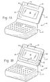
- Fig. 1a shows, by way of example of the preferred embodiment of the invention, a device 10, such as a pager, incorporating an antenna as according to the present invention.
- the device includes a lid 12 and a body 14.
- the lid 12 preferably includes an LCD display 16 for displaying both incoming and outgoing alphanumeric data.
- the body 14 receives and retains the electronic components that process the device signal and provide other device functions.
- Antenna 20 is preferably incorporated into the device lid 14 and thus hidden from view.
- Figure 1b shows two antennae 30 in a configuration designed for either simultaneous transmission and reception of data or to reduce the design requirements imposed by a single antenna structure.
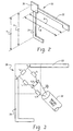
- antenna 20 is a dipole formed of a horizontal arm 22 and a vertical arm 24 for receiving the signal in each of the vertical and horizontal polarization planes.
- the respective dipole arms 22, 24 are sized to fit within the device lid 12, and in the case of the dual antenna configuration, are placed in such a manner that each antenna 30 is conductively isolated from the other.
- the arms 22, 24 are preferably made of copper and have a thickness of about 0.0025" on a 0.001" Kapton material substrate.
- the horizontal arm 22 is preferably about 2.04" in length with an extending portion of about 0.54".
- the vertical arm 24 is preferably about 2.17" long, with a lower portion about 1.19" in length.
- the horizontal arm and the vertical arm are substantially orthogonal, i.e. they form a substantially 90° angle.
- the position of the arms need only to be at an angle such that the two arms are not in the same line.
- antenna 20 is two-dimensional in shape, it can transmit and receive signals in both planes of polarization (as shown in Fig. 2), thus enabling a device, such as a device to be less sensitive to tilting and orientation and to provide excellent in-building performance.
- the preferred construction of dipole antenna 20 results in a gain of about 0dB at 900MHz, at least a 5dB improvement in gain over the previous loop-type antenna frequently used in pagers.
- the data signal is reciprocally processed through an LC lumped matching circuit 30, as shown in Fig. 3, that preferably includes capacitors (C1, C2) and inductors (L1, L2, L3) for connecting the dipole arms 22, 24 to a coaxial cable within the device body 14.
- C1 4.3pF
- C2 7.5pF
- L3 4.7nH
- the coaxial cable is a MXFX81 cable and display 16, which also can affect the values of C1, C2, L1, L2 and L3, is preferably a FSTN LCD available from Varitronix, Hong Kong as part no. CRUS 1024-V05.
- LC circuit 30 provides transformer action, matching action and balancing action, as will be shown subsequently.
- LC circuit 30 provides an impedance to antenna 20 to match the 50 ohm impedance of the RF device contained within device body 14. This impedance matching reduces currents induced on the device components by the presence of a human operator and various ground plane conditions, thereby improving the gain of the device.
- the present matching circuit also provides a transformer action wherein the signal energy is proportioned between each of the arms.
- an RF signal is fed through a coaxial cable 32 into the circuit 30 where it is split into each of the arms 22, 24 where the signal is transformed to electromagnetic radiation which propagates through the air.
- the matching circuit 30 combines the signals received and transforms the RF signal to a detectable level. The detectable signal then travels through the coaxial cable to the RF data communications device.
- the performance of the present antenna is greatly facilitated by the coupling between the dipole arms 22, 24.
- Applicants have discovered that the presence of an anisotropic medium in proximity with the antenna is effective at controlling the electrical environment within the device and affecting the propagation vector of the antenna.
- the liquid crystal material in the present LCD 16 is anisotropic, and as applicants have discovered, its anisotropic nature provides the desired coupling properties.
- the present "coupling" is analogous to the mutual inductance in a transformer, where electromagnetic energy propagates across a pair of the inductors in respective resonating circuits.
- the two dipole arms 22, 24 can be electromagnetically coupled as are the inductors in a transformer.
- the anisotropic material of the LCD 16 creates a non-uniform electric field effectively splitting the signal transmitted and received from each dipole element into perpendicular components.
- the signal propagated from the horizontal dipole 22 propagates in a horizontal polarization.
- a portion of the signal propagating through the LCD 16 is transformed into the vertical polarization, so that the original polarized wave is effectively split into waves having vertical and horizontal polarization.
- the polarized signal propagating from the vertical dipole 24 is split into perpendicular components.
- the electromagnetic coupling through the LCD 16 is such that each of these respective perpendicular components reinforce each other in phase, so that constructive wave fronts are produced for each polarization. In this way, each of the respective dipoles 22, 24 are electromagnetically coupled.
- Under-coupling of the dipoles occurs when the mutual effects of each dipole element on the respective other produce a single resonant amplitude peak.
- Critical-coupling results in a single resonant mode with maximum amplitude about a central frequency.
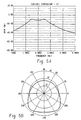
- the resonant response of under-coupled and critically-coupled antennae is shown in Fig. 4A.
- These couplings also result in a spatial amplitude peak as shown in Fig. 4B., in which antenna gain peaks around 230 degrees (where zero is the forward facing direction of the user.)
- Antenna performance as according to the preferred embodiment occurs when coupling is further increased so that the dipole becomes overcoupled.
- the resonant amplitude of an overcoupled dipole resonates at two peak frequencies of equal amplitude, with respective peaks representing the symmetrical and antisymmetrical modes centered about a desired base frequency, as shown in Fig. 5A. This results in an effectively broadened resonant frequency bandwidth.
- the frequency peaks are birefringent, i.e., each has a propagation vector perpendicular to the other.
- the overcoupled dipole thus propagates two perpendicular signals differing only slightly in resonant symmetrical and antisymmetrical frequency.
- the result is an antenna with a broadened effective bandwidth in both polarizations, thus increasing the antenna gain.
- the overcoupled dipole also resonates with two spatial amplitude peaks, as seen in Fig. 5B.
- the gain is thus higher over a larger perimeter of the user, and therefore the present antenna is less sensitive to directional variations in gain.
- Dipole 20 and matching circuit 30 cooperate to enable a two-way RF data communications device that is stable and insensitive against antenna detuning in the ambient environment. Antenna detuning can occur from, among many causes, parasitic capacitance and adverse ground plane conditions. Also, the present invention is insensitive to directional orientation and signal deflections within buildings. The present invention offers at least a 5dB improvement in gain over previous loop antennae and at least a 3db improvement in gain over patch antennae used in hand-held data communications devices and an operative bandwidth at about 10% as compared with 1-2% for other one-way devices and 1/2% for other two-way devices.
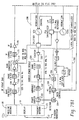
- FIG. 6A shows a simple block diagram of an RF data communications device, such as a pager, which incorporates the instant invention.
- a control subsystem 200 comprising a DSP 130, memory 140 and control 150; a radio receiver 110 and a radio transmitter 120; and the antenna system 170 of the instant invention comprising a dipole antenna 20 in conjunction with a matching circuit, and LCD display 16 that, as discussed above, serves the dual function of displaying data as a part of data interface 160 and as an anisotropic medium for electromagnetic coupling of the signals radiating from the arms of the dipole antenna 20.
- Switch/Duplexer 175 represents the element that places the antenna system 170 in either a transmit or receive mode. Although shown as part of antenna system 20, switch/duplexer 175 could just as easily be represented and configured as an element that functions outside antenna system 20, but operatively connected to it. Figure 7A, discussed in greater detail below, illustrates the placement of the switch/duplexer 175 outside the antenna subsystem. Additionally, the function that switch/duplexer 175 performs could be performed with a electronic, software or mechanical switch, or a duplexer or by any means by which different data streams, one in-bound and one out-bound can be separated and either transmitted or received, as relevant, over the dipole antenna 20.
- Figure 6B differs from Figure 6A only in its use of a dual antenna system 171.
- Receive antenna 28 and transmit antenna 29 replace the single dipole antenna 20 to enable the RF data communications device to transmit and receive simultaneously or to reduce the design requirements associated with a single antenna configuration.
- This configuration eliminates the need for the switch/duplexer 175 found in Figure 6, because each mode is accommodated by a separate antenna in this configuration.
- FIGS 7A and 7B are more detailed versions of the RF communications devices shown in Figures 6A and 6B, respectively.
- Antenna 20 and Display 16 are represented in Antenna/Display Subsystem 600.
- Radio Receiver 110 is represented by items 111-117, IQ demodulator 118, auxiliary local oscillator synthesizer 119 and local oscillator synthesizer 200, which Radio Receiver 110 shares with Radio Transmitter 120.
- Radio Transmitter 120 includes items 311-314, 321-324, 330-336, clock circuit 210, and local oscillator synthesizer 200, which it shares with Radio Receiver 110.
- Memory 140 is represented by flash RAM 141 and SRAM 142.
- Control 150 is represented by microprocessor 500 in conjunction with control line 151.
- Data Interface is represented by serial line 161 in conjunction with microprocessor 500.
- display 16 could also be consider part of the data interface 160. Additionally, any input device, such as a keyboard, mouse, touchscreen, etc., would be considered part of data
- Figures 7A and 7B illustrate other components of the RF data communications device.
- Items 601 and 602 represent the circuitry for processing data from Battery Voltage Sensor 603.
- Items 701 and 702 represent the circuitry for processing data from Temperature Sensor 703. Also included in the device is Power Management Circuitry 100.
- Figure 7B differs from Figure 7A only in that it includes a dual antenna configuration represented by Receive Antenna 28 and Transmit Antenna 29.
- switch/duplexer 175 comprising T/R switch 176 is no longer needed.
- the receive circuit and the transmit circuit share Local Oscillator Synthesizer 200, it is not possible for this device to utilize the dual antenna structure to transmit and receive simultaneously. By replicating the functions that are share by including an additional local oscillator synthesizer, one can easily see that the use of dual antennae would enable, in that instance, simultaneous transmission and reception.
- the present invention solves many problems associated with previous antennae used with RF data transmission and presents improved efficiency and operability.
- the preferred embodiment of the invention has been described in reference to a pager, the invention has applicability to any device that has the need for an antenna system that solves many problems found in prior art antennae.
- the devices to which the antenna system of the instant invention can be applied are notebook computers, combined cell phones and pagers, PDA's, PIM's and other personal data devices, including those worn on the wrist, in conjunction with eyeglasses or as a belt around the body.
Landscapes
- Engineering & Computer Science (AREA)
- Computer Hardware Design (AREA)
- General Engineering & Computer Science (AREA)
- Support Of Aerials (AREA)
- Mobile Radio Communication Systems (AREA)
- Transceivers (AREA)
- Input Circuits Of Receivers And Coupling Of Receivers And Audio Equipment (AREA)
- Radar Systems Or Details Thereof (AREA)
- Near-Field Transmission Systems (AREA)
Abstract
Description
Claims (11)
- Antenna system for enhancing the performance of an RF data communications device, comprising a dipole antenna (20; 28, 29) having a first arm (22) extending in a first direction and a second arm (24) extending in a second direction that is not in the same line as the first direction,
characterized by :an electromagnetic coupler comprising an anisotropic medium (16) placed in proximity to the dipole antenna (20; 28, 29), wherein the electromagnetic coupler balances the signal strength between the first arm (22) and the second arm (24) and establishes a desired resonant bandwidth for operating the RF data communications device; andan impedance matching circuit (30) including at least one capacitor element and at least one inductor element, wherein the impedance matching circuit (30) matches the impedance of the RF data communications device to which the antenna (20; 28, 29) is operatively connected. - Antenna system according to claim 1, characterized in that the anisotropic medium comprises a liquid crystal display (16).
- Antenna system according to claim 1, characterized in that the impedance matching circuit is a lumped LC circuit (30).
- Antenna system according to claim 3, characterized in that the values of each inductor and each capacitor are selected to provide impedance matching and a balanced to unbalanced transformation between the dipole antenna (20; 28, 29) and the RF data communications device.
- Antenna system according to claim 1, characterized in that the dipole antenna is a first dipole antenna (28) and the antenna system further comprises a second dipole antenna (29) placed in proximity to the first dipole antenna (28) and to the electromagnetic coupler.
- RF data communications device with improved antenna performance, comprising:characterized in that the antenna system further comprises:a data interface (160);a radio receiver (110);a radio transmitter (120), whereinthe data interface (160), radio receiver (110) and radio transmitter (120) are connected through a microprocessor (130); andan antenna system, wherein the antenna system comprises a dipole antenna (20; 28, 29) having a first arm (22) extending in a first direction and a second arm (24) extending in a second direction that is not in the same line as the first direction,an electromagnetic coupler comprising an anisotropic medium (16) placed in proximity to the dipole antenna (20; 28, 29), wherein the electromagnetic coupler balances the signal strength between the first arm (22) and the second arm (24) and establishes a desired resonant bandwidth for operating the RF data communications device; andan impedance matching circuit (30) including at least one capacitor element and at least one inductor element, wherein the impedance matching circuit (30) matches the impedance of the RF data communications device to which the antenna (20; 28, 29) is operatively connected.
- RF data communications device according to claim 6, characterized in that it further comprises a transmit/receive switch (175), wherein the switch (175) switches the mode of the antenna system from transmission to reception and from reception to transmission, the dipole antenna (20; 28, 29) is used for transmitting when the switch (175) has switched the mode of the antenna system to transmission and the dipole antenna (20; 28, 29) is used for receiving when the switch (20; 28, 29) has switched the mode of the antenna system to reception.
- RF data communications device according to claim 7, characterized in that the transmit/receive switch is a duplexer (175).
- RF data communications device according to claim 6, characterized in that the dipole antenna is a first dipole antenna (28) and the antenna system further comprises a second dipole antenna (29) placed in proximity to the first dipole antenna (28) and to the electromagnetic coupler.
- RF data communications device according to claim 9, characterized in that RF signal reception occurs through the first dipole antenna (28) and RF signal transmission occurs through the second dipole antenna (29).
- Method of enhancing performance of an antenna associated with an RF data communications device, characterized by the following steps:placing an anisotropic medium (16) between two arms (22, 24) of a dipole antenna (20; 28, 29); andelectromagnetically coupling the anisotropic medium (16) and the dipole antenna (20; 28, 29) so as to split signals radiating from each dipole antenna arm (22, 24) into orthogonal components to create a desired resonant bandwidth.
Applications Claiming Priority (3)
| Application Number | Priority Date | Filing Date | Title |
|---|---|---|---|
| US715347 | 1996-09-18 | ||
| US08/715,347 US5966098A (en) | 1996-09-18 | 1996-09-18 | Antenna system for an RF data communications device |
| PCT/CA1997/000671 WO1998012771A1 (en) | 1996-09-18 | 1997-09-17 | Antenna system for an rf data communications device |
Publications (2)
| Publication Number | Publication Date |
|---|---|
| EP0927435A1 EP0927435A1 (en) | 1999-07-07 |
| EP0927435B1 true EP0927435B1 (en) | 2002-07-31 |
Family
ID=24873667
Family Applications (1)
| Application Number | Title | Priority Date | Filing Date |
|---|---|---|---|
| EP97939924A Expired - Lifetime EP0927435B1 (en) | 1996-09-18 | 1997-09-17 | Antenna system for an rf data communications device |
Country Status (10)
| Country | Link |
|---|---|
| US (1) | US5966098A (en) |
| EP (1) | EP0927435B1 (en) |
| KR (1) | KR100304152B1 (en) |
| CN (1) | CN1107990C (en) |
| AT (1) | ATE221700T1 (en) |
| AU (1) | AU713890B2 (en) |
| CA (1) | CA2265948C (en) |
| DE (1) | DE69714452T2 (en) |
| TW (1) | TW381381B (en) |
| WO (1) | WO1998012771A1 (en) |
Families Citing this family (81)
| Publication number | Priority date | Publication date | Assignee | Title |
|---|---|---|---|---|
| SE511131C2 (en) * | 1997-11-06 | 1999-08-09 | Ericsson Telefon Ab L M | Portable electronic communication device with multi-band antenna system |
| US6489950B1 (en) | 1998-06-26 | 2002-12-03 | Research In Motion Limited | Hand-held electronic device with auxiliary input device |
| US6278442B1 (en) * | 1998-06-26 | 2001-08-21 | Research In Motion Limited | Hand-held electronic device with a keyboard optimized for use with the thumbs |
| US7705828B2 (en) * | 1998-06-26 | 2010-04-27 | Research In Motion Limited | Dual-mode mobile communication device |
| US6357887B1 (en) | 1999-05-14 | 2002-03-19 | Apple Computers, Inc. | Housing for a computing device |
| US6977808B2 (en) | 1999-05-14 | 2005-12-20 | Apple Computer, Inc. | Display housing for computing device |
| JP2001016019A (en) * | 1999-06-29 | 2001-01-19 | Murata Mfg Co Ltd | Portable terminal device |
| DE29925006U1 (en) | 1999-09-20 | 2008-04-03 | Fractus, S.A. | Multilevel antenna |
| ES2205898T3 (en) | 1999-10-26 | 2004-05-01 | Fractus, S.A. | MULTIBAND CLUSTERS OF INTERRELATED ANTENNAS. |
| CN100373693C (en) | 2000-01-19 | 2008-03-05 | 弗拉克托斯股份有限公司 | Space-filling small antenna |
| JP2003520542A (en) * | 2000-01-19 | 2003-07-02 | フラクトゥス・ソシエダッド・アノニマ | Fractal and space-filled transmission lines, resonators, filters and elements for passive networks |
| WO2001057950A1 (en) * | 2000-02-07 | 2001-08-09 | Qualcomm Incorporated | Balanced antenna system for portable computers |
| US6329951B1 (en) * | 2000-04-05 | 2001-12-11 | Research In Motion Limited | Electrically connected multi-feed antenna system |
| EP1313166B1 (en) * | 2000-04-19 | 2007-11-14 | Advanced Automotive Antennas, S.L. | Multilevel advanced antenna for motor vehicles |
| TW447169B (en) * | 2000-04-20 | 2001-07-21 | Hon Hai Prec Ind Co Ltd | Antenna module unit |
| KR100708085B1 (en) | 2000-05-31 | 2007-04-16 | 삼성전자주식회사 | Omnidirectional Antenna Systems and Notebook Computers |
| US6339400B1 (en) * | 2000-06-21 | 2002-01-15 | International Business Machines Corporation | Integrated antenna for laptop applications |
| GB0015374D0 (en) * | 2000-06-23 | 2000-08-16 | Koninkl Philips Electronics Nv | Antenna arrangement |
| US6307520B1 (en) | 2000-07-25 | 2001-10-23 | International Business Machines Corporation | Boxed-in slot antenna with space-saving configuration |
| US6531985B1 (en) * | 2000-08-14 | 2003-03-11 | 3Com Corporation | Integrated laptop antenna using two or more antennas |
| JP4522564B2 (en) * | 2000-09-22 | 2010-08-11 | 富士通株式会社 | Electronics |
| JP2002100887A (en) * | 2000-09-25 | 2002-04-05 | Toshiba Corp | Electronics |
| US7511675B2 (en) | 2000-10-26 | 2009-03-31 | Advanced Automotive Antennas, S.L. | Antenna system for a motor vehicle |
| US20020111194A1 (en) * | 2000-12-11 | 2002-08-15 | Farbod Behbahani | Laptop wireless systems integrated with an LCD panel |
| US6434372B1 (en) | 2001-01-12 | 2002-08-13 | The Regents Of The University Of California | Long-range, full-duplex, modulated-reflector cell phone for voice/data transmission |
| EP1358696A1 (en) | 2001-02-07 | 2003-11-05 | Fractus, S.A. | Miniature broadband ring-like microstrip patch antenna |
| US6904296B2 (en) * | 2001-02-09 | 2005-06-07 | Nokia Mobile Phones Limited | Internal antenna for mobile communications device |
| SE524825C2 (en) * | 2001-03-07 | 2004-10-12 | Smarteq Wireless Ab | Antenna coupling device cooperating with an internal first antenna arranged in a communication device |
| TW490879B (en) * | 2001-03-09 | 2002-06-11 | Hon Hai Prec Ind Co Ltd | Antenna |
| US6664930B2 (en) | 2001-04-12 | 2003-12-16 | Research In Motion Limited | Multiple-element antenna |
| DE10119531A1 (en) * | 2001-04-12 | 2002-10-24 | Siemens Ag | Mobile computer or PDA with a radio or mobile communications module has the aerial integrated into the device lid, so that when it is opened out for use, the aerial is an optimum operating position |
| CN1507673A (en) | 2001-04-16 | 2004-06-23 | �����ɷ� | Dual-band dual-polarized antenna array |
| JP4588921B2 (en) * | 2001-05-21 | 2010-12-01 | 富士通コンポーネント株式会社 | Input device |
| US6686886B2 (en) * | 2001-05-29 | 2004-02-03 | International Business Machines Corporation | Integrated antenna for laptop applications |
| US7766517B2 (en) | 2001-06-15 | 2010-08-03 | Apple Inc. | Active enclosure for computing device |
| US7452098B2 (en) | 2001-06-15 | 2008-11-18 | Apple Inc. | Active enclosure for computing device |
| CA2447545C (en) * | 2001-06-15 | 2010-03-30 | Apple Computer, Inc. | Active enclosure for computing device |
| JP3670987B2 (en) * | 2001-08-13 | 2005-07-13 | インターナショナル・ビジネス・マシーンズ・コーポレーション | ANTENNA UNIT AND COMPUTER TERMINAL HAVING THE SAME |
| WO2003034545A1 (en) | 2001-10-16 | 2003-04-24 | Fractus, S.A. | Multifrequency microstrip patch antenna with parasitic coupled elements |
| EP1444751B1 (en) * | 2001-10-16 | 2007-06-13 | Fractus, S.A. | Loaded antenna |
| WO2003034544A1 (en) | 2001-10-16 | 2003-04-24 | Fractus, S.A. | Multiband antenna |
| US9755314B2 (en) | 2001-10-16 | 2017-09-05 | Fractus S.A. | Loaded antenna |
| US6842169B2 (en) | 2001-10-19 | 2005-01-11 | Research In Motion Limited | Hand-held electronic device with multiple input mode thumbwheel |
| US6567056B1 (en) * | 2001-11-13 | 2003-05-20 | Intel Corporation | High isolation low loss printed balun feed for a cross dipole structure |
| ES2190749B1 (en) | 2001-11-30 | 2004-06-16 | Fractus, S.A | "CHAFF" MULTINIVEL AND / OR "SPACE-FILLING" DISPERSORS, AGAINST RADAR. |
| US20030125969A1 (en) * | 2001-12-28 | 2003-07-03 | Wireless Checking, Inc. | Method and apparatus for processing financial transactions over a paging network |
| US6879293B2 (en) * | 2002-02-25 | 2005-04-12 | Tdk Corporation | Antenna device and electric appliance using the same |
| DE60329793D1 (en) * | 2002-06-21 | 2009-12-03 | Research In Motion Ltd | Multiple element antenna with parasitic coupler |
| US7301783B2 (en) * | 2002-09-05 | 2007-11-27 | Hewlett-Packard Development Company, L.P. | Computing device having an antenna |
| US6791500B2 (en) | 2002-12-12 | 2004-09-14 | Research In Motion Limited | Antenna with near-field radiation control |
| CA2414718C (en) | 2002-12-17 | 2005-11-22 | Research In Motion Limited | Dual mode antenna system for radio transceiver |
| EP2273611B1 (en) | 2002-12-22 | 2012-02-08 | Fractus, S.A. | Multi-band monopole antenna for a mobile communications device |
| US6842149B2 (en) * | 2003-01-24 | 2005-01-11 | Solectron Corporation | Combined mechanical package shield antenna |
| JP2004318466A (en) * | 2003-04-16 | 2004-11-11 | Matsushita Electric Ind Co Ltd | Gift certificate, gift certificate issuing system and gift certificate use system |
| EP1478047B1 (en) | 2003-05-14 | 2007-10-03 | Research In Motion Limited | Antenna with multiple-band patch and slot structures |
| EP1912279B1 (en) * | 2003-06-12 | 2011-01-05 | Research In Motion Limited | Multiple-element antenna with electromagnetically coupled floating antenna element |
| US6980173B2 (en) * | 2003-07-24 | 2005-12-27 | Research In Motion Limited | Floating conductor pad for antenna performance stabilization and noise reduction |
| EP1709704A2 (en) | 2004-01-30 | 2006-10-11 | Fractus, S.A. | Multi-band monopole antennas for mobile communications devices |
| DE102004008929A1 (en) * | 2004-02-24 | 2005-09-01 | Bayerische Motoren Werke Ag | Vehicle tires with steel belt wires and a arranged in the tread area dipole antenna |
| JP2005295312A (en) * | 2004-04-01 | 2005-10-20 | Hitachi Ltd | Portable wireless device |
| US7369089B2 (en) * | 2004-05-13 | 2008-05-06 | Research In Motion Limited | Antenna with multiple-band patch and slot structures |
| US7193581B2 (en) * | 2004-06-01 | 2007-03-20 | Miltope Corporation | Electronic equipment shock isolation/protection bumper, with integrated antenna |
| KR100678275B1 (en) * | 2004-06-19 | 2007-02-02 | 삼성전자주식회사 | Antenna module |
| EP1771814B1 (en) * | 2004-07-20 | 2008-10-29 | Nxp B.V. | Multipurpose antenna configuration for a contactless data carrier |
| US9130602B2 (en) | 2006-01-18 | 2015-09-08 | Qualcomm Incorporated | Method and apparatus for delivering energy to an electrical or electronic device via a wireless link |
| US8447234B2 (en) | 2006-01-18 | 2013-05-21 | Qualcomm Incorporated | Method and system for powering an electronic device via a wireless link |
| US8738103B2 (en) | 2006-07-18 | 2014-05-27 | Fractus, S.A. | Multiple-body-configuration multimedia and smartphone multifunction wireless devices |
| US9774086B2 (en) | 2007-03-02 | 2017-09-26 | Qualcomm Incorporated | Wireless power apparatus and methods |
| KR101335824B1 (en) * | 2007-04-19 | 2013-12-03 | 엘지전자 주식회사 | Mobile terminal |
| US9124120B2 (en) | 2007-06-11 | 2015-09-01 | Qualcomm Incorporated | Wireless power system and proximity effects |
| JP5697979B2 (en) | 2007-08-09 | 2015-04-08 | クゥアルコム・インコーポレイテッドQualcomm Incorporated | System and method for wireless powering and charging |
| JP2010539857A (en) * | 2007-09-17 | 2010-12-16 | クゥアルコム・インコーポレイテッド | Transmitter and receiver for wireless energy transmission |
| EP2208279A4 (en) | 2007-10-11 | 2016-11-30 | Qualcomm Inc | Wireless power transfer using magneto mechanical systems |
| US7845066B2 (en) * | 2007-10-22 | 2010-12-07 | Auden Techno Corp. | Method of installing an antenna of a notebook computer |
| US8629576B2 (en) | 2008-03-28 | 2014-01-14 | Qualcomm Incorporated | Tuning and gain control in electro-magnetic power systems |
| US8559869B2 (en) | 2011-09-21 | 2013-10-15 | Daniel R. Ash, JR. | Smart channel selective repeater |
| FR3004738B1 (en) | 2013-04-19 | 2015-05-15 | Musthane | ANCHORING ASSEMBLY |
| US9601267B2 (en) | 2013-07-03 | 2017-03-21 | Qualcomm Incorporated | Wireless power transmitter with a plurality of magnetic oscillators |
| CN105305017A (en) * | 2014-06-26 | 2016-02-03 | 展讯通信(上海)有限公司 | Mobile terminal |
| WO2018126247A2 (en) | 2017-01-02 | 2018-07-05 | Mojoose, Inc. | Automatic signal strength indicator and automatic antenna switch |
| US12625528B2 (en) * | 2024-04-24 | 2026-05-12 | Dell Products L.P. | Couple fed corner frame antenna in an information handling system |
Family Cites Families (9)
| Publication number | Priority date | Publication date | Assignee | Title |
|---|---|---|---|---|
| US3599214A (en) * | 1969-03-10 | 1971-08-10 | New Tronics Corp | Automobile windshield antenna |
| US4584709A (en) * | 1983-07-06 | 1986-04-22 | Motorola, Inc. | Homotropic antenna system for portable radio |
| IT8353707V0 (en) * | 1983-09-12 | 1983-09-12 | Sant Andrea Novara Officine | COMB HEAD WITH CHAIN CONTROL FOR TEXTILE FIBER BELTS, PARTICULARLY FOR IRONING |
| US4571595A (en) * | 1983-12-05 | 1986-02-18 | Motorola, Inc. | Dual band transceiver antenna |
| GB2257838B (en) * | 1991-07-13 | 1995-06-14 | Technophone Ltd | Retractable antenna |
| US5138328A (en) * | 1991-08-22 | 1992-08-11 | Motorola, Inc. | Integral diversity antenna for a laptop computer |
| JPH05335826A (en) * | 1991-11-18 | 1993-12-17 | Motorola Inc | Built-in antenna for communication equipment |
| US5373300A (en) * | 1992-05-21 | 1994-12-13 | International Business Machines Corporation | Mobile data terminal with external antenna |
| US5684672A (en) * | 1996-02-20 | 1997-11-04 | International Business Machines Corporation | Laptop computer with an integrated multi-mode antenna |
-
1996
- 1996-09-18 US US08/715,347 patent/US5966098A/en not_active Expired - Lifetime
-
1997
- 1997-09-17 DE DE69714452T patent/DE69714452T2/en not_active Expired - Lifetime
- 1997-09-17 CA CA002265948A patent/CA2265948C/en not_active Expired - Fee Related
- 1997-09-17 CN CN97198020A patent/CN1107990C/en not_active Expired - Fee Related
- 1997-09-17 AU AU41970/97A patent/AU713890B2/en not_active Ceased
- 1997-09-17 WO PCT/CA1997/000671 patent/WO1998012771A1/en not_active Ceased
- 1997-09-17 AT AT97939924T patent/ATE221700T1/en not_active IP Right Cessation
- 1997-09-17 EP EP97939924A patent/EP0927435B1/en not_active Expired - Lifetime
- 1997-10-01 TW TW086114315A patent/TW381381B/en not_active IP Right Cessation
-
1999
- 1999-03-17 KR KR1019997002245A patent/KR100304152B1/en not_active Expired - Fee Related
Also Published As
| Publication number | Publication date |
|---|---|
| WO1998012771A1 (en) | 1998-03-26 |
| AU713890B2 (en) | 1999-12-16 |
| CA2265948A1 (en) | 1998-03-26 |
| US5966098A (en) | 1999-10-12 |
| DE69714452T2 (en) | 2003-05-08 |
| CA2265948C (en) | 2001-04-10 |
| CN1231069A (en) | 1999-10-06 |
| DE69714452D1 (en) | 2002-09-05 |
| TW381381B (en) | 2000-02-01 |
| ATE221700T1 (en) | 2002-08-15 |
| HK1021259A1 (en) | 2000-06-02 |
| KR20000036190A (en) | 2000-06-26 |
| EP0927435A1 (en) | 1999-07-07 |
| CN1107990C (en) | 2003-05-07 |
| KR100304152B1 (en) | 2001-09-29 |
| AU4197097A (en) | 1998-04-14 |
Similar Documents
| Publication | Publication Date | Title |
|---|---|---|
| AU713890B2 (en) | Antenna system for an RF data communications device | |
| EP1295358B1 (en) | Convertible loop/inverted-f antennas and wireless communicators incorporating the same | |
| US6282433B1 (en) | Personal communication terminal with a slot antenna | |
| US6662028B1 (en) | Multiple frequency inverted-F antennas having multiple switchable feed points and wireless communicators incorporating the same | |
| US6271796B1 (en) | Built-in antenna for radio communication terminals | |
| US7053843B2 (en) | Multi-band antenna system | |
| US6198442B1 (en) | Multiple frequency band branch antennas for wireless communicators | |
| US6229487B1 (en) | Inverted-F antennas having non-linear conductive elements and wireless communicators incorporating the same | |
| US20050128162A1 (en) | Antenna | |
| TW201220737A (en) | Communication device | |
| US6563466B2 (en) | Multi-frequency band inverted-F antennas with coupled branches and wireless communicators incorporating same | |
| WO2006032965A1 (en) | Terminal and associated transducer assembly and method for selectively transducing in at least two frequency bands | |
| EP1154513A1 (en) | Built-in antenna of wireless communication terminal | |
| Salonen et al. | A novel Bluetooth antenna on flexible substrate for smart clothing | |
| US6445906B1 (en) | Micro-slot antenna | |
| US20060142072A1 (en) | Portable communication device with global positioning system antenna | |
| CA2328825C (en) | Antenna system for an rf data communications device | |
| CA2351304C (en) | Antenna system for an rf data communications device | |
| HK1021259B (en) | Antenna system for an rf data communications device | |
| US6968203B2 (en) | Device for mobile terminal | |
| CN112151954A (en) | Housing assembly, electronic device, and method for adjusting dielectric constant of housing assembly | |
| US20030132881A1 (en) | Double F antenna | |
| US7146201B2 (en) | Portable wireless apparatus | |
| CN117913526A (en) | Antenna components and electronic devices |
Legal Events
| Date | Code | Title | Description |
|---|---|---|---|
| PUAI | Public reference made under article 153(3) epc to a published international application that has entered the european phase |
Free format text: ORIGINAL CODE: 0009012 |
|
| 17P | Request for examination filed |
Effective date: 19990316 |
|
| AK | Designated contracting states |
Kind code of ref document: A1 Designated state(s): AT BE CH DE FR GB IE LI NL SE |
|
| RIN1 | Information on inventor provided before grant (corrected) |
Inventor name: CARKNER, STEVEN Inventor name: EDMONSON, PETER Inventor name: JARMUSZEWSKI, PERRY Inventor name: QI, YIHONG Inventor name: ZHU, LIZHONG |
|
| 17Q | First examination report despatched |
Effective date: 20000710 |
|
| GRAG | Despatch of communication of intention to grant |
Free format text: ORIGINAL CODE: EPIDOS AGRA |
|
| GRAG | Despatch of communication of intention to grant |
Free format text: ORIGINAL CODE: EPIDOS AGRA |
|
| GRAH | Despatch of communication of intention to grant a patent |
Free format text: ORIGINAL CODE: EPIDOS IGRA |
|
| GRAH | Despatch of communication of intention to grant a patent |
Free format text: ORIGINAL CODE: EPIDOS IGRA |
|
| GRAA | (expected) grant |
Free format text: ORIGINAL CODE: 0009210 |
|
| AK | Designated contracting states |
Kind code of ref document: B1 Designated state(s): AT BE CH DE FR GB IE LI NL SE |
|
| PG25 | Lapsed in a contracting state [announced via postgrant information from national office to epo] |
Ref country code: NL Free format text: LAPSE BECAUSE OF FAILURE TO SUBMIT A TRANSLATION OF THE DESCRIPTION OR TO PAY THE FEE WITHIN THE PRESCRIBED TIME-LIMIT Effective date: 20020731 Ref country code: LI Free format text: LAPSE BECAUSE OF FAILURE TO SUBMIT A TRANSLATION OF THE DESCRIPTION OR TO PAY THE FEE WITHIN THE PRESCRIBED TIME-LIMIT Effective date: 20020731 Ref country code: CH Free format text: LAPSE BECAUSE OF FAILURE TO SUBMIT A TRANSLATION OF THE DESCRIPTION OR TO PAY THE FEE WITHIN THE PRESCRIBED TIME-LIMIT Effective date: 20020731 Ref country code: BE Free format text: LAPSE BECAUSE OF FAILURE TO SUBMIT A TRANSLATION OF THE DESCRIPTION OR TO PAY THE FEE WITHIN THE PRESCRIBED TIME-LIMIT Effective date: 20020731 Ref country code: AT Free format text: LAPSE BECAUSE OF FAILURE TO SUBMIT A TRANSLATION OF THE DESCRIPTION OR TO PAY THE FEE WITHIN THE PRESCRIBED TIME-LIMIT Effective date: 20020731 |
|
| REF | Corresponds to: |
Ref document number: 221700 Country of ref document: AT Date of ref document: 20020815 Kind code of ref document: T |
|
| REG | Reference to a national code |
Ref country code: GB Ref legal event code: FG4D Ref country code: CH Ref legal event code: EP |
|
| REG | Reference to a national code |
Ref country code: IE Ref legal event code: FG4D |
|
| REF | Corresponds to: |
Ref document number: 69714452 Country of ref document: DE Date of ref document: 20020905 |
|
| PG25 | Lapsed in a contracting state [announced via postgrant information from national office to epo] |
Ref country code: IE Free format text: LAPSE BECAUSE OF NON-PAYMENT OF DUE FEES Effective date: 20020917 |
|
| ET | Fr: translation filed | ||
| NLV1 | Nl: lapsed or annulled due to failure to fulfill the requirements of art. 29p and 29m of the patents act | ||
| REG | Reference to a national code |
Ref country code: CH Ref legal event code: PL |
|
| PLBE | No opposition filed within time limit |
Free format text: ORIGINAL CODE: 0009261 |
|
| STAA | Information on the status of an ep patent application or granted ep patent |
Free format text: STATUS: NO OPPOSITION FILED WITHIN TIME LIMIT |
|
| REG | Reference to a national code |
Ref country code: IE Ref legal event code: MM4A |
|
| 26N | No opposition filed |
Effective date: 20030506 |
|
| REG | Reference to a national code |
Ref country code: DE Ref legal event code: R082 Ref document number: 69714452 Country of ref document: DE Representative=s name: MERH-IP MATIAS ERNY REICHL HOFFMANN, DE |
|
| REG | Reference to a national code |
Ref country code: DE Ref legal event code: R082 Ref document number: 69714452 Country of ref document: DE Representative=s name: MERH-IP MATIAS ERNY REICHL HOFFMANN PATENTANWA, DE Effective date: 20140925 Ref country code: DE Ref legal event code: R082 Ref document number: 69714452 Country of ref document: DE Representative=s name: MERH-IP MATIAS ERNY REICHL HOFFMANN, DE Effective date: 20140925 Ref country code: DE Ref legal event code: R081 Ref document number: 69714452 Country of ref document: DE Owner name: BLACKBERRY LIMITED, WATERLOO, CA Free format text: FORMER OWNER: RESEARCH IN MOTION LTD., WATERLOO, ONTARIO, CA Effective date: 20140925 |
|
| REG | Reference to a national code |
Ref country code: FR Ref legal event code: PLFP Year of fee payment: 19 |
|
| PGFP | Annual fee paid to national office [announced via postgrant information from national office to epo] |
Ref country code: GB Payment date: 20150928 Year of fee payment: 19 |
|
| PGFP | Annual fee paid to national office [announced via postgrant information from national office to epo] |
Ref country code: FR Payment date: 20150917 Year of fee payment: 19 Ref country code: SE Payment date: 20150929 Year of fee payment: 19 |
|
| PGFP | Annual fee paid to national office [announced via postgrant information from national office to epo] |
Ref country code: DE Payment date: 20150929 Year of fee payment: 19 |
|
| REG | Reference to a national code |
Ref country code: DE Ref legal event code: R119 Ref document number: 69714452 Country of ref document: DE |
|
| PG25 | Lapsed in a contracting state [announced via postgrant information from national office to epo] |
Ref country code: SE Free format text: LAPSE BECAUSE OF NON-PAYMENT OF DUE FEES Effective date: 20160918 |
|
| REG | Reference to a national code |
Ref country code: SE Ref legal event code: EUG |
|
| GBPC | Gb: european patent ceased through non-payment of renewal fee |
Effective date: 20160917 |
|
| REG | Reference to a national code |
Ref country code: FR Ref legal event code: ST Effective date: 20170531 |
|
| PG25 | Lapsed in a contracting state [announced via postgrant information from national office to epo] |
Ref country code: FR Free format text: LAPSE BECAUSE OF NON-PAYMENT OF DUE FEES Effective date: 20160930 Ref country code: DE Free format text: LAPSE BECAUSE OF NON-PAYMENT OF DUE FEES Effective date: 20170401 Ref country code: GB Free format text: LAPSE BECAUSE OF NON-PAYMENT OF DUE FEES Effective date: 20160917 |