EP0926817B1 - Improved feedforward multicarrier linear RF power amplifier - Google Patents
Improved feedforward multicarrier linear RF power amplifier Download PDFInfo
- Publication number
- EP0926817B1 EP0926817B1 EP98309989A EP98309989A EP0926817B1 EP 0926817 B1 EP0926817 B1 EP 0926817B1 EP 98309989 A EP98309989 A EP 98309989A EP 98309989 A EP98309989 A EP 98309989A EP 0926817 B1 EP0926817 B1 EP 0926817B1
- Authority
- EP
- European Patent Office
- Prior art keywords
- module
- circuitry
- components
- power
- amplifier
- Prior art date
- Legal status (The legal status is an assumption and is not a legal conclusion. Google has not performed a legal analysis and makes no representation as to the accuracy of the status listed.)
- Expired - Lifetime
Links
- 230000001419 dependent effect Effects 0.000 claims description 8
- 238000004519 manufacturing process Methods 0.000 claims description 8
- 238000012937 correction Methods 0.000 claims description 5
- 238000000034 method Methods 0.000 claims description 5
- 230000003321 amplification Effects 0.000 claims description 4
- 238000012544 monitoring process Methods 0.000 claims description 4
- 238000003199 nucleic acid amplification method Methods 0.000 claims description 4
- 238000013461 design Methods 0.000 description 23
- 238000010586 diagram Methods 0.000 description 4
- 230000005540 biological transmission Effects 0.000 description 3
- 238000013459 approach Methods 0.000 description 2
- 239000002184 metal Substances 0.000 description 2
- 238000000638 solvent extraction Methods 0.000 description 2
- 238000010348 incorporation Methods 0.000 description 1
- 230000001788 irregular Effects 0.000 description 1
- 238000002955 isolation Methods 0.000 description 1
- 230000007257 malfunction Effects 0.000 description 1
- 230000000737 periodic effect Effects 0.000 description 1
- 238000005204 segregation Methods 0.000 description 1
- 238000012876 topography Methods 0.000 description 1
Images


Classifications
-
- H—ELECTRICITY
- H03—ELECTRONIC CIRCUITRY
- H03F—AMPLIFIERS
- H03F1/00—Details of amplifiers with only discharge tubes, only semiconductor devices or only unspecified devices as amplifying elements
- H03F1/32—Modifications of amplifiers to reduce non-linear distortion
- H03F1/3241—Modifications of amplifiers to reduce non-linear distortion using predistortion circuits
-
- H—ELECTRICITY
- H04—ELECTRIC COMMUNICATION TECHNIQUE
- H04W—WIRELESS COMMUNICATION NETWORKS
- H04W88/00—Devices specially adapted for wireless communication networks, e.g. terminals, base stations or access point devices
- H04W88/08—Access point devices
Definitions
- This invention relates to multicarrier linear RF power amplifiers, and to methods of making same.
- Fig. 1 depicts a schematic diagram of a portion of a typical wireless communications system in the prior art.
- a system provides wireless telecommunications service to a number of wireless terminals (e.g., wireless terminals 101-1 through 103-1) that are situated within a geographic region.
- Wireless Switching Center 120 which may also be known as a Mobile Switching Center (“MSC”) or a Mobile Telephone Switching Office (“MTSO”).
- WSC Wireless Switching Center
- MSC Mobile Switching Center
- MTSO Mobile Telephone Switching Office
- Wireless Switching Center 120 is connected to a plurality of base stations (e.g., base stations 103-1 through 103-5) that are dispersed throughout the geographic area serviced by the system.
- Wireless Switching Center 120 is connected to local- and toll-offices (e.g., local-office 130, local-office 138 and toll-office 140).
- Wireless Switching Center 120 is responsible for, among other things, establishing and maintaining calls between wireless terminals and between a wireless terminal and a wireline terminal, which is connected to the system via the local and/or long-distance networks.
- each cell is schematically represented by a hexagon; in practice, however, each cell usually has an irregular shape that depends on terrain topography.
- each cell contains a base station, which comprises radios and antennas that the base station uses to communicate with the wireless terminals in that cell and also comprises the transmission equipment that the base station uses to communicate with WSC 120.
- wireless terminal 101-1 desires to communicate with wireless terminal 101-2
- wireless terminal 101-1 transmits the desired information to base station 103-1, which relays the information to WSC 120.
- WSC 120 Upon receiving the information, and with the knowledge that it is intended for wireless terminal 101-2, WSC 120 then returns the information back to base station 103-1, which relays the information, via radio, to wireless terminal 101-2.
- the radio modulates the information onto a RF carrier signal in accordance with the particular modulation scheme of the wireless system (e.g., time-division-multiple-access, code-division-multiple-access, etc. ).
- the modulated output RF signal from the radio is a very low power signal that requires amplification for transmission from base station 103-1 to wireless terminal 101-2.
- a feedforward multicarrier linear RF power amplifier can be used to amplify the output signal from the radio. In fact, such an amplifier can usually amplify all of the RF carrier signals in use within a given cell.
- the design and operation of linear amplifiers are known in the art. See , for example, U.S. Pat. No. 5,304,945, which is incorporated by reference herein.
- linear amplifier circuit 200 includes several splitters (202, 220), gain & phase control circuitry (204, 224), couplers (214, 216, 222, 228), delay circuitry (210, 218), a correction amplifier (226), pre-distortion driver circuitry (206), the main amplifier (208) and processor control circuitry (212).
- the various circuits of a conventional linear amplifier are typically interspersed within a large housing that is designed to support the weight of the main amplifier, dissipate heat and prevent RF from radiating to the external environment. Additionally, the various individual circuits are housed in metal boxes or "clam shells" to provide RF isolation.
- Modularization is a technique that may be used to achieve such ends.
- components or circuits of a device are segregated into modules based on one or more underlying criteria.
- modularization can be based on segregating components that generate noise from components that are sensitive to noise, or segregating components that generate heat from non heat-generating components, or segregating components requiring access for initial or periodic adjustment from those that do not, or segregating components based on weight or size considerations, to mention just a few.
- a desirable approach is one that reduces the cost of designing and manufacturing the amplifier, that reduces the time to deliver the amplifier for a specific service, and one that simplifies field servicing of the amplifier.
- EP-A-0 289 130 discloses a radio transmitter having pre-distortion circuits that are selectively connectable between the mixing stages of the transmitter and the final power-amplifying stage.
- the choice f which pre-distortion circuit to connect is determined based on the RF frequency of the signal to be transmitted.
- EP-A-0 714 164 discloses feed-forward, linear, radio-frequency amplifiers, which contain components which can be grouped into two categories: active and passive. All active components are constructed as two-port devices, which are easily tested, using standard equipment, in order to locate malfunctions. The active components plug into a network of the passive components, comprising striplines, waveguides, coaxial cables, and the like.
- an improved feedforward multicarrier linear RF power amplifier advantageously comprises several modules. Each of such modules contains a portion of the circuitry of a conventional MLRF power amp.
- the circuitry of a standard FMLRF power amp has advantageously been partitioned into modules such that: (1) high power components are segregated from low power components; and (2) components operating within a narrow frequency range are segregated from those having broadband frequency operation. Additionally, the circuitry is advantageously partitioned to result in a few simple RF interfaces between the modules.
- an improved FMLRF power amp having three modules including: (i) a RF power module; (ii) a linearizer module; and (iii) a DC power supply module.
- the RF power module primarily contains amplification circuitry. Such circuitry is operating frequency dependent and, of course, dependent on the desired RF output power leveL
- the design of the RF power module may vary from amplifier to amplifier as a function of the operating frequency requirements (a range defined, collectively, by the frequency of each of the RF carrier signals in use within a cell) and the output power requirements for a given application.
- the linearizer module contains broadband low-power level RF circuits and control circuits. Such circuitry is substantially operating-frequency and power-level independent. In contrast to the RF power module, the linearizer module will not vary from amplifier to amplifier. In other words, it contains "generic" circuitry such that a single design suffices for substantially any application.
- the DC power supply module supplies power to the FMLRF power amp. It is not required when an external power supply is available.
- the DC power supply module contains power-level dependent but frequency-independent components. The DC power supply does not vary from amplifier to amplifier unless there is a substantial change in RF output power level between such amplifiers.
- An improved FMLRF power amp in accordance with the illustrated embodiments advantageously reduces design cost, time to market and manufacturing cost of a FMLRF power amplifier.
- new FMLRF power amps can be "designed” and “manufactured” by simply selecting "off-the-shelf” modules where appropriate. Where such off-the-shelf modules are not suitable because, for example, of a variance in RF power output requirements, a new RF power module design may be all that is required. The necessity of a designing a new linearizer module, which is the most difficult circuitry of the amplifier to design and manufacture, is usually avoided.
- FIG. 3 depicts a schematic diagram of an illustrative embodiment of the present invention, wherein FMLRF power amp 300 is advantageously partitioned into modules by segregating circuitry and components according to at least the following two criteria. First, high power circuitry and components are segregated from low power circuitry and components. And second, narrow (frequency) band circuits and components are segregated from broadband circuits and components. Additionally, the modules resulting from the segregation of circuitry and components must be interconnectable by a few simply- implemented interfaces.
- Segregating the circuitry and components of a FMLRF power amp according to the above guidelines advantageously results, in some embodiments, in four modules.
- the four modules include linearizer module 310, RF power module 320, DC power supply module 330 and alarm and control module 340.
- a primary function of the circuitry within linearizer module 310 is to attenuate distortion generated by the main amplifier (component 208 in FIG. 2) within RF power module 320.
- Linearizer module 310 contains broadband, low power circuitry and components.
- Linearizer module 310 includes splitters 202 and 220, gain & phase control circuitry 204, 224, delay circuitry 210, coupler 216 and processor control circuitry 212 (see FIG. 2).
- Such circuitry and components are substantially power independent in the sense that a single design suffices regardless of amplifier output power.
- such circuitry and components are substantially frequency independent in the sense that their broadband operating frequency range overlaps that of substantially any likely RF carrier frequency.
- a single design of linearizer module 310 may be advantageously used for most applications.
- linearizer module 310 advantageously includes port 312 for receiving an RF input signal, interface 314 for receiving a portion of an amplified signal from RF power module 320 and for delivering a signal thereto, interface 316 for receiving power from DC power supply 330 and interface 318 for electrical connection with alarm and control module 340.
- interface 314 receives: (i) a first signal from coupler 214 (in RF power module 320) and delivers it to splitter 216, and (ii) a second signal from coupler 228 (in RF power module 320) and delivers it to processor control 212.
- interface 314 delivers: (i) a third signal from gain & phase control 204 to pre-distortion driver 206 (in RF power module 320), and (ii) a fourth signal from gain & phase control 224 to correction amplifier 226 (in RF power module 320).
- a primary function of circuitry within RF power module 320 is to amplify the RF input signal after it is processed in linearizer module 310.
- RF power module 320 contains narrow frequency band, high power circuitry and components.
- RF power module 320 includes pre-distortion driver 206, amplifer 208, couplers 214, 222, 228, delay circuitry 218 and correction amplifier 226 (see FIG. 2).
- circuitry and components in the RF power module are substantially power dependent in the sense that module design varies as a function of desired amplifier output power.
- such circuitry and components are substantially frequency dependent in the sense that due to their relatively narrow range in operating frequency, design changes may be required with each application ( e.g., use within a different base station).
- RF power module 320 advantageously includes interface 322 for sending a portion of the amplified RF signal to linearizer module 310, interface 324 for receiving power from DC power supply 330, interface 326 for electrical connection with alarm and control module 340 and port 328 for delivering the amplified RF signal to an antenna for transmission.
- DC power supply module 330 provides power to linearizer module 310, RF power module 320 and alarm and control module 340. Circuitry and components within DC power supply module 330 are somewhat dependent upon the output power of RF power module 320, but substantially frequency independent. Large changes in amplifier output power may require a change in the design of the DC power supply module.
- DC power supply module 330 advantageously includes interfaces 332, 334 and 336 for supplying power to the other modules. External power input 338 supplies power to DC power supply module 330. For applications in which an external power supply is available, DC power supply module 330 is not required. Those familiar with the design of multicarrier linear RF power amplifiers will be able to construct a DC power supply module in accordance with the present teachings.
- Alarm and control module 340 monitors desired systems within FMLRF power amp 300.
- the alarm and control module is programmable to accomodate changes in monitoring requirements. In embodiments having minimal monitoring requirements, alarm and control module 340 may not required.
- the alarm and control module includes power and frequency insensitive components. As such, module design does not vary with amplifier requirements.
- the circuitry and components comprising alarm and control module 340 can be incorporated in linearizer module 310. Such incorporation is consistent within the above-described partitioning criteria ( i . e ., the circuitry of both the linearizer and the alarm and control module is independent of amplifier output power and operating frequency).
- alarm and control module 340 advantageously includes interface 342 in electrical connection with interface 318 on the linearizer module, interface 344 in electrical connection with interface 336 on the DC power supply module and interface 346 in electrical connection with interface 326 of the RF power module.
- interfaces allow alarm and control module 340 to monitor conditions within the various modules and take appropriate actions ( e . g ., shutdown, etc.).
- Alarm and control module 340 further advantageously includes external interfaces 348 for monitoring system conditions external to the other modules. Those familiar with the design of multicarrier linear RF power amplifiers will be able to construct an alarm and control module in accordance with the present teachings.
- Partitioning the FMLRF power amp 300 as described above advantageously reduces the cost and time to design and manufacture an amplifier for a given application.
- design and manufacture of a FMLRF power amp reduces to the simple act of selecting, if available, an off-the-shelf RF power module having the desired output power.
- the linearizer module and alarm and control module design are substantially invariant; a single design being suitable for most applications. Only a few DC power supply module designs should suffice for a broad range of RF power module designs. If required, a RF power module can be rapidly designed and manufactured relative to the time required for the design and manufacture of a conventional feedforward multicarrier linear RF power amplifier.
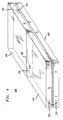
- FIG. 4 depicts a perspective view of interconnected modules of an illustrative embodiment of the present invention.
- a FMLRF 400 comprises three modules, including linearizer module 410, RF power module 420 and DC power supply module 430.
- the alarm and control module circuitry, not shown, is included in linearizer module 410.
- Linearizer module 410 and RF power module 420 are electrically connected at interfaces 314 and 322.
- the linearizer module is electrically connected to DC power supply module 430 at interfaces 316 and 332.
- the RF power module is electrically connected to the DC power supply module at interfaces 324 and 334.
- the module enclosures are advantageously formed of metal to provide shielding to circuits and components therein.
Landscapes
- Engineering & Computer Science (AREA)
- Physics & Mathematics (AREA)
- Nonlinear Science (AREA)
- Power Engineering (AREA)
- Computer Networks & Wireless Communication (AREA)
- Signal Processing (AREA)
- Amplifiers (AREA)
- Mobile Radio Communication Systems (AREA)
- Microwave Amplifiers (AREA)
Description
- This invention relates to multicarrier linear RF power amplifiers, and to methods of making same.
- Fig. 1 depicts a schematic diagram of a portion of a typical wireless communications system in the prior art. Such a system provides wireless telecommunications service to a number of wireless terminals (e.g., wireless terminals 101-1 through 103-1) that are situated within a geographic region.
- The heart of a typical wireless telecommunications system is Wireless Switching Center ("WSC")120, which may also be known as a Mobile Switching Center ("MSC") or a Mobile Telephone Switching Office ("MTSO"). Typically, Wireless Switching Center 120 is connected to a plurality of base stations (e.g., base stations 103-1 through 103-5) that are dispersed throughout the geographic area serviced by the system. Additionally, Wireless Switching Center 120 is connected to local- and toll-offices (e.g., local-
office 130, local-office 138 and toll-office 140). Wireless Switching Center 120 is responsible for, among other things, establishing and maintaining calls between wireless terminals and between a wireless terminal and a wireline terminal, which is connected to the system via the local and/or long-distance networks. - The geographic area serviced by a wireless telecommunications system is partitioned into a number of spatially-distinct areas called "cells." As depicted in FIG. 1, each cell is schematically represented by a hexagon; in practice, however, each cell usually has an irregular shape that depends on terrain topography. Typically, each cell contains a base station, which comprises radios and antennas that the base station uses to communicate with the wireless terminals in that cell and also comprises the transmission equipment that the base station uses to communicate with
WSC 120. - For example, when wireless terminal 101-1 desires to communicate with wireless terminal 101-2, wireless terminal 101-1 transmits the desired information to base station 103-1, which relays the information to
WSC 120. Upon receiving the information, and with the knowledge that it is intended for wireless terminal 101-2, WSC 120 then returns the information back to base station 103-1, which relays the information, via radio, to wireless terminal 101-2. - To relay information, the radio modulates the information onto a RF carrier signal in accordance with the particular modulation scheme of the wireless system (e.g., time-division-multiple-access, code-division-multiple-access, etc.). The modulated output RF signal from the radio is a very low power signal that requires amplification for transmission from base station 103-1 to wireless terminal 101-2.
- A feedforward multicarrier linear RF power amplifier can be used to amplify the output signal from the radio. In fact, such an amplifier can usually amplify all of the RF carrier signals in use within a given cell. The design and operation of linear amplifiers are known in the art. See, for example, U.S. Pat. No. 5,304,945, which is incorporated by reference herein.
- Unfortunately, conventional feedforward multicarrier linear RF power amplifiers are very complex and costly, both to design and manufacture. And, each application requires a custom design dictated by a variety of system requirements. Conventional feedforward multicarrier linear RF power amplifiers have been designed using a combination of RF circuits, analog control circuits and digital control circuits. A simplified schematic of
linear amplifier circuit 200 is shown in FIG. 2. As depicted in FIG. 2,linear amplifier circuit 200 includes several splitters (202, 220), gain & phase control circuitry (204, 224), couplers (214, 216, 222, 228), delay circuitry (210, 218), a correction amplifier (226), pre-distortion driver circuitry (206), the main amplifier (208) and processor control circuitry (212). - The various circuits of a conventional linear amplifier are typically interspersed within a large housing that is designed to support the weight of the main amplifier, dissipate heat and prevent RF from radiating to the external environment. Additionally, the various individual circuits are housed in metal boxes or "clam shells" to provide RF isolation.
- It would be desirable to reduce the cost and complexity of such amplifiers. Modularization is a technique that may be used to achieve such ends. When modularizing, components or circuits of a device are segregated into modules based on one or more underlying criteria It will be appreciated that, as a complex electronic device comprised of a myriad of circuits, there are potentially numerous ways to modularize a feedforward multicarrier linear RF power amplifier. For example, modularization can be based on segregating components that generate noise from components that are sensitive to noise, or segregating components that generate heat from non heat-generating components, or segregating components requiring access for initial or periodic adjustment from those that do not, or segregating components based on weight or size considerations, to mention just a few.
- Such varied approaches will yield varied results in terms of the utility of the modularized amplifier. A desirable approach is one that reduces the cost of designing and manufacturing the amplifier, that reduces the time to deliver the amplifier for a specific service, and one that simplifies field servicing of the amplifier.
- EP-A-0 289 130 discloses a radio transmitter having pre-distortion circuits that are selectively connectable between the mixing stages of the transmitter and the final power-amplifying stage. The choice f which pre-distortion circuit to connect is determined based on the RF frequency of the signal to be transmitted.
- EP-A-0 714 164 discloses feed-forward, linear, radio-frequency amplifiers, which contain components which can be grouped into two categories: active and passive. All active components are constructed as two-port devices, which are easily tested, using standard equipment, in order to locate malfunctions. The active components plug into a network of the passive components, comprising striplines, waveguides, coaxial cables, and the like.
- As amplifier and a method according to the invention are as set out in the independent claims. Preferred forms are set out in the dependent claims.
- In accordance with the illustrative embodiments of the present invention, an improved feedforward multicarrier linear RF power amplifier ("FMLRF power amp") advantageously comprises several modules. Each of such modules contains a portion of the circuitry of a conventional MLRF power amp.
- In some embodiments, the circuitry of a standard FMLRF power amp has advantageously been partitioned into modules such that: (1) high power components are segregated from low power components; and (2) components operating within a narrow frequency range are segregated from those having broadband frequency operation. Additionally, the circuitry is advantageously partitioned to result in a few simple RF interfaces between the modules.
- Segregating the circuitry of a conventional FMLRF power amp to satisfy the above-listed criteria advantageously results, in some embodiments, in an improved FMLRF power amp having three modules including: (i) a RF power module; (ii) a linearizer module; and (iii) a DC power supply module.
- The RF power module primarily contains amplification circuitry. Such circuitry is operating frequency dependent and, of course, dependent on the desired RF output power leveL The design of the RF power module may vary from amplifier to amplifier as a function of the operating frequency requirements (a range defined, collectively, by the frequency of each of the RF carrier signals in use within a cell) and the output power requirements for a given application.
- The linearizer module contains broadband low-power level RF circuits and control circuits. Such circuitry is substantially operating-frequency and power-level independent. In contrast to the RF power module, the linearizer module will not vary from amplifier to amplifier. In other words, it contains "generic" circuitry such that a single design suffices for substantially any application. The DC power supply module supplies power to the FMLRF power amp. It is not required when an external power supply is available. The DC power supply module contains power-level dependent but frequency-independent components. The DC power supply does not vary from amplifier to amplifier unless there is a substantial change in RF output power level between such amplifiers.
- An improved FMLRF power amp in accordance with the illustrated embodiments advantageously reduces design cost, time to market and manufacturing cost of a FMLRF power amplifier. In accordance with the illustrated embodiments, new FMLRF power amps can be "designed" and "manufactured" by simply selecting "off-the-shelf" modules where appropriate. Where such off-the-shelf modules are not suitable because, for example, of a variance in RF power output requirements, a new RF power module design may be all that is required. The necessity of a designing a new linearizer module, which is the most difficult circuitry of the amplifier to design and manufacture, is usually avoided.
-
- FIG. 1 depicts a schematic diagram of a prior art wireless telecommunication system;
- FIG. 2 depicts a schematic diagram of a prior art linear amplifier circuit;
- FIG. 3 depicts an illustrative embodiment of the present invention wherein a feedforward multicarrier linear RF amplifier is modularly partitioned; and
- FIG. 4 depicts a perspective view of a feedforward multicarrier linear RF amplifier in accordance with the illustrative embodiment of the present invention.
-
- FIG. 3 depicts a schematic diagram of an illustrative embodiment of the present invention, wherein
FMLRF power amp 300 is advantageously partitioned into modules by segregating circuitry and components according to at least the following two criteria. First, high power circuitry and components are segregated from low power circuitry and components. And second, narrow (frequency) band circuits and components are segregated from broadband circuits and components. Additionally, the modules resulting from the segregation of circuitry and components must be interconnectable by a few simply- implemented interfaces. - Segregating the circuitry and components of a FMLRF power amp according to the above guidelines advantageously results, in some embodiments, in four modules. The four modules include
linearizer module 310,RF power module 320, DCpower supply module 330 and alarm andcontrol module 340. - A primary function of the circuitry within
linearizer module 310 is to attenuate distortion generated by the main amplifier (component 208 in FIG. 2) withinRF power module 320.Linearizer module 310 contains broadband, low power circuitry and components.Linearizer module 310 includessplitters phase control circuitry delay circuitry 210,coupler 216 and processor control circuitry 212 (see FIG. 2). Such circuitry and components are substantially power independent in the sense that a single design suffices regardless of amplifier output power. Moreover, such circuitry and components are substantially frequency independent in the sense that their broadband operating frequency range overlaps that of substantially any likely RF carrier frequency. In view of the power level and frequency range independence of the components and circuits contained withinlinearizer module 310, a single design oflinearizer module 310 may be advantageously used for most applications. - In the illustrated embodiment,
linearizer module 310 advantageously includesport 312 for receiving an RF input signal,interface 314 for receiving a portion of an amplified signal fromRF power module 320 and for delivering a signal thereto,interface 316 for receiving power fromDC power supply 330 andinterface 318 for electrical connection with alarm andcontrol module 340. With reference to FIG. 2,interface 314 receives: (i) a first signal from coupler 214 (in RF power module 320) and delivers it tosplitter 216, and (ii) a second signal from coupler 228 (in RF power module 320) and delivers it toprocessor control 212. Additionally,interface 314 delivers: (i) a third signal from gain &phase control 204 to pre-distortion driver 206 (in RF power module 320), and (ii) a fourth signal from gain &phase control 224 to correction amplifier 226 (in RF power module 320). - A primary function of circuitry within
RF power module 320 is to amplify the RF input signal after it is processed inlinearizer module 310.RF power module 320 contains narrow frequency band, high power circuitry and components.RF power module 320 includespre-distortion driver 206,amplifer 208,couplers delay circuitry 218 and correction amplifier 226 (see FIG. 2). Unlike the circuitry and components inlinearizer module 310, circuitry and components in the RF power module are substantially power dependent in the sense that module design varies as a function of desired amplifier output power. Moreover, such circuitry and components are substantially frequency dependent in the sense that due to their relatively narrow range in operating frequency, design changes may be required with each application (e.g., use within a different base station). - In the illustrated embodiment,
RF power module 320 advantageously includesinterface 322 for sending a portion of the amplified RF signal tolinearizer module 310,interface 324 for receiving power fromDC power supply 330,interface 326 for electrical connection with alarm andcontrol module 340 andport 328 for delivering the amplified RF signal to an antenna for transmission. - DC
power supply module 330 provides power tolinearizer module 310,RF power module 320 and alarm andcontrol module 340. Circuitry and components within DCpower supply module 330 are somewhat dependent upon the output power ofRF power module 320, but substantially frequency independent. Large changes in amplifier output power may require a change in the design of the DC power supply module. In the illustrated embodiment, DCpower supply module 330 advantageously includesinterfaces External power input 338 supplies power to DCpower supply module 330. For applications in which an external power supply is available, DCpower supply module 330 is not required. Those familiar with the design of multicarrier linear RF power amplifiers will be able to construct a DC power supply module in accordance with the present teachings. - Alarm and
control module 340 monitors desired systems withinFMLRF power amp 300. In some embodiments, the alarm and control module is programmable to accomodate changes in monitoring requirements. In embodiments having minimal monitoring requirements, alarm andcontrol module 340 may not required. The alarm and control module includes power and frequency insensitive components. As such, module design does not vary with amplifier requirements. In some embodiments, the circuitry and components comprising alarm andcontrol module 340 can be incorporated inlinearizer module 310. Such incorporation is consistent within the above-described partitioning criteria (i.e., the circuitry of both the linearizer and the alarm and control module is independent of amplifier output power and operating frequency). - In the illustrated embodiment, alarm and
control module 340 advantageously includesinterface 342 in electrical connection withinterface 318 on the linearizer module,interface 344 in electrical connection withinterface 336 on the DC power supply module andinterface 346 in electrical connection withinterface 326 of the RF power module. Such interfaces allow alarm andcontrol module 340 to monitor conditions within the various modules and take appropriate actions (e.g., shutdown, etc.). Alarm andcontrol module 340 further advantageously includesexternal interfaces 348 for monitoring system conditions external to the other modules. Those familiar with the design of multicarrier linear RF power amplifiers will be able to construct an alarm and control module in accordance with the present teachings. - Partitioning the
FMLRF power amp 300 as described above advantageously reduces the cost and time to design and manufacture an amplifier for a given application. For some applications, design and manufacture of a FMLRF power amp reduces to the simple act of selecting, if available, an off-the-shelf RF power module having the desired output power. As previously noted, the linearizer module and alarm and control module design are substantially invariant; a single design being suitable for most applications. Only a few DC power supply module designs should suffice for a broad range of RF power module designs. If required, a RF power module can be rapidly designed and manufactured relative to the time required for the design and manufacture of a conventional feedforward multicarrier linear RF power amplifier. - FIG. 4 depicts a perspective view of interconnected modules of an illustrative embodiment of the present invention. In the embodiment shown in FIG. 4, a
FMLRF 400 comprises three modules, includinglinearizer module 410,RF power module 420 and DCpower supply module 430. The alarm and control module circuitry, not shown, is included inlinearizer module 410.Linearizer module 410 andRF power module 420 are electrically connected atinterfaces power supply module 430 atinterfaces interfaces - Although specific embodiments of this invention have been shown and described herein, it is to be understood that these embodiments are merely illustrative of the many possible specific arrangements that can be devised in application of the principles of the invention. Numerous and varied other arrangements can be devised in accordance with these principles by those of ordinary skill in the art without departing from the scope of the invention. It is therefore intended that such other arrangements be included within the scope of the following claims and their equivalents.
Claims (11)
- A feedforward, multicarrier, linear RF power amplifier for amplifying, with a first amount of distortion, a multicarrier RF signal, wherein:circuitry and components that compose said multicarrier linear RF power amplifier are segregated into:a first module (320) comprising a first group of said circuitry and components, wherein:said first group adapted to amplify said multicarrier RF signal with a second amount of distortion that is greater than the first amount;said first group including only narrow-frequency band and high-power circuitry and components; andsaid first group contained in a first module enclosure (420); anda second module (310) comprising a second group of said circuitry and components, wherein:said second group adapted to attenuate distortion caused that would otherwise be generated during amplification of said multicarrier RF carrier signal in said first module;said second group including only broad-frequency band and low-power circuitry and components; andsaid second group contained in a second module enclosure (410); anda first interface (322) electrically connecting said first module (320) to said second module (310) so that said first module (320) and said second module (310) collectively amplify said multicarrier RF signal with said first amount of distortion, when powered.
- An amplifier as claimed in claim 1, wherein:the frequency band of said narrow-frequency band and high-power circuitry and components is dictated by RF carrier frequency; andthe power of said narrow-frequency band and high-power circuitry and components is dictated by RF output power requirements.
- An amplifier as claimed in claim 2 comprising a second interface (316), wherein:said second interface electrically connects said second module (310) to a DC power supply module (330); andsaid DC power supply module comprises a third portion of said circuitry and components, which third portion is adapted to supply power to said second module.
- An amplifier as claimed in claim 3 comprising said DC power supply module (330), wherein:said DC power supply module is electrically connected to said second interface (316);said third circuitry and components are substantially independent of RF carrier frequency and dependent on RF output power requirements; andsaid third circuitry and components are contained within a third one (430) of said module enclosures.
- An amplifier as claimed in claim 1 comprising an alarm and control module (340), wherein:said alarm and control module is electrically connected to said RF power module (320) and said second module (310);said alarm and control module comprises fourth circuitry and components for monitoring said second circuitry and components of said second module (310) and said first circuitry and components of said first module (320);said fourth circuitry and components are substantially independent of RF carrier frequency and RF output power requirements; andsaid fourth circuitry and components are contained within a fourth of said module enclosures.
- An amplifier as claimed in claim 2 wherein said first circuitry and components of said first module (320) comprise:wherein said first circuitry and components of said linearizer module (310) comprise:a main amplifier (208);a pre-distortion driver (206) electrically connected to said main amplifier (208);a first coupler (214) electrically connected to said main amplifier (208);a first delay circuit (218) electrically connected to said first coupler (214);a second coupler (222) electrically connected to said first delay circuit (218);a correction amplifier (226) electrically connected to said second coupler (222); anda third coupler (228) electrically connected to said second coupler (222); andwherein said processor control circuitry (212) is electrically connected to said first gain and phase control circuit (204) and said second gain and phase control circuit (224).a first splitter (202) for receiving the RF carrier signal;a first gain and phase control circuit (204) electrically connected to said first splitter (202);a second delay circuit (210) electrically connected to said first gain and phase control circuit (204);a second splitter (216) electrically connected to said second delay circuit (210);a third splitter (220) electrically connected to said second splitter (216);processor control circuitry (212) electrically connected to said third splitter (220); anda second gain and phase control circuit (224) electrically connected to said third splitter (220);
- An amplifier as claimed in claim 6 wherein electrical connection between said second module (310) and said first module (320) comprises:a first electrical connection between an output of said first gain and phase control circuit (204) in said second module (310) and a first input of said pre-distortion driver (206) in said first module (320);a second electrical connection between at least a first output of said processor control circuit (212) in said second module (310) and a second input of the said pre-distortion driver (206) in said first module (320);a third electrical connection between a first output of said pre-distortion driver (206) in said first module (320) and a first input of said processor control circuit (212) in the second module (310);a fourth electrical connection between a first output of said third coupler (228) in said first module (320) and a second input of said processor control circuit (212) in said second module (310);a fifth electrical connection between a first output of the second gain and phase control circuit (224) in the second module (310) and an input of the correction amplifier (226) in the first module (320); anda sixth electrical connection between an output of the first coupler of the first module (320) and an input of said second splitter (216) in said second module (310).
- An amplifier as claimed in claim 2 wherein said second module enclosure (410) abuts said first module enclosure (420).
- An amplifier as claimed in claim 4 wherein said DC power module enclosure (430) abuts said first module enclosure (420).
- A method of making a feedforward, multicarrier, linear RF power amplifier, said amplifier being for amplifying, with a first amount of distortion, a multicarrier RF signal, the method comprising:segregating circuitry and components that compose said feedforward multicarrier linear RF power amplifier into:a first module (320) comprising a first group of said circuitry and components, wherein:said first group adapted to amplify said multicarrier RF signal with a second amount of distortion that is greater than the first amount;said first group including only narrow-frequency band and high-power circuitry and components; andsaid first group contained in a first module enclosure (420); anda second module (310) comprising a second group of said circuitry and components, wherein:said second group adapted to attenuate distortion caused that would otherwise be generated during amplification of said multicarrier RF carrier signal in said first module;said second group including only broad-frequency band and low-power circuitry and components; andsaid second group contained in a second module enclosure (410); andelectrically connecting said first module (320) and said second module (310) so that said first module (320) and said second module (310) collectively amplify said multicarrier RF signal with said first amount of distortion, when powered.
- A method as claimed in claim 10 comprising electrically connecting said first module (320) and said second module (310) to a third module (330), wherein said third module (330) comprises a DC power supply, and wherein said DC power supply is contained within a third module enclosure (430).
Applications Claiming Priority (2)
| Application Number | Priority Date | Filing Date | Title |
|---|---|---|---|
| US993682 | 1997-12-18 | ||
| US08/993,682 US6057733A (en) | 1997-12-18 | 1997-12-18 | Feedforward multicarrier linear RF power amplifier |
Publications (2)
| Publication Number | Publication Date |
|---|---|
| EP0926817A1 EP0926817A1 (en) | 1999-06-30 |
| EP0926817B1 true EP0926817B1 (en) | 2005-02-16 |
Family
ID=25539824
Family Applications (1)
| Application Number | Title | Priority Date | Filing Date |
|---|---|---|---|
| EP98309989A Expired - Lifetime EP0926817B1 (en) | 1997-12-18 | 1998-12-04 | Improved feedforward multicarrier linear RF power amplifier |
Country Status (8)
| Country | Link |
|---|---|
| US (1) | US6057733A (en) |
| EP (1) | EP0926817B1 (en) |
| JP (1) | JP3440011B2 (en) |
| KR (1) | KR19990063256A (en) |
| CN (1) | CN1156073C (en) |
| CA (1) | CA2254456C (en) |
| DE (1) | DE69829036T2 (en) |
| TW (1) | TW425757B (en) |
Families Citing this family (9)
| Publication number | Priority date | Publication date | Assignee | Title |
|---|---|---|---|---|
| US6255903B1 (en) * | 1999-12-06 | 2001-07-03 | Motorola | Linear power amplifier with configurable feedforward error correction circuits |
| EP1170860A1 (en) * | 2000-06-27 | 2002-01-09 | Nortel Matra Cellular | Improved multi-carrier receiver for radio telecommunications network |
| US6747879B2 (en) * | 2001-02-28 | 2004-06-08 | Andrew Corporation | High power amplifier and chassis |
| US6760230B2 (en) | 2001-02-28 | 2004-07-06 | Andrew Corporation | Compact, high efficiency, high isolation power amplifier |
| US6801086B1 (en) * | 2002-04-03 | 2004-10-05 | Andrew Corporation | Adaptive digital pre-distortion using amplifier model that incorporates frequency-dependent non-linearities |
| US6700439B2 (en) | 2002-04-11 | 2004-03-02 | Andrew Corporation | Zero-bias bypass switch |
| US6812786B2 (en) | 2002-04-11 | 2004-11-02 | Andrew Corporation | Zero-bias bypass switching circuit using mismatched 90 degrees hybrid |
| JP4896424B2 (en) * | 2005-04-22 | 2012-03-14 | 株式会社日立国際電気 | Distortion compensation amplifier |
| JP4909417B2 (en) | 2007-01-17 | 2012-04-04 | テレフオンアクチーボラゲット エル エム エリクソン(パブル) | Apparatus and method for controlling an antenna system in a communication system |
Family Cites Families (13)
| Publication number | Priority date | Publication date | Assignee | Title |
|---|---|---|---|---|
| US4472725A (en) * | 1982-02-01 | 1984-09-18 | Century Iii Electronics Inc. | LC Delay line for feedforward amplifier |
| US4625178A (en) * | 1985-07-19 | 1986-11-25 | General Instrument Corporation | Feedforward gain block with mirror image error amplifier |
| US4782307A (en) * | 1987-06-08 | 1988-11-01 | Hughes Aircraft Company | Feed-forward microwave amplifier arrangement with ferrite temperature compensation |
| US4943783A (en) | 1989-07-31 | 1990-07-24 | Nippon Telegraph And Telephone Corporation | Feed forward distortion correction circuit |
| CA2046413C (en) * | 1990-07-11 | 1994-01-04 | Shoichi Narahashi | Feed-forward amplifier |
| US5524285A (en) * | 1993-11-02 | 1996-06-04 | Wray; Anthony J. | Radio transmitter with power amplifier and linearization |
| US5455537A (en) * | 1994-08-19 | 1995-10-03 | Radio Frequency Systems, Inc. | Feed forward amplifier |
| DE4432119A1 (en) * | 1994-09-09 | 1996-03-14 | Telefunken Sendertechnik | Air-cooled transmitter amplifier |
| US5523716A (en) * | 1994-10-13 | 1996-06-04 | Hughes Aircraft Company | Microwave predistortion linearizer |
| US5955916A (en) * | 1994-11-23 | 1999-09-21 | Lucent Technologies Inc. | Modulator linear feed-forward amplifier |
| US5913163A (en) * | 1996-03-14 | 1999-06-15 | Telefonaktiebolaget Lm Ericsson | Integrated local communication system |
| US5774018A (en) * | 1996-09-18 | 1998-06-30 | Hughes Electronics Corporation | Linear amplifier system and method |
| US5789978A (en) * | 1996-11-25 | 1998-08-04 | Space Systems/Loral, Inc. | Ku-band linearizer bridge |
-
1997
- 1997-12-18 US US08/993,682 patent/US6057733A/en not_active Expired - Lifetime
-
1998
- 1998-11-25 CA CA002254456A patent/CA2254456C/en not_active Expired - Fee Related
- 1998-12-01 TW TW087119917A patent/TW425757B/en active
- 1998-12-04 DE DE69829036T patent/DE69829036T2/en not_active Expired - Lifetime
- 1998-12-04 EP EP98309989A patent/EP0926817B1/en not_active Expired - Lifetime
- 1998-12-17 KR KR1019980056588A patent/KR19990063256A/en not_active Ceased
- 1998-12-17 CN CNB981255833A patent/CN1156073C/en not_active Expired - Fee Related
- 1998-12-17 JP JP35944698A patent/JP3440011B2/en not_active Expired - Fee Related
Also Published As
| Publication number | Publication date |
|---|---|
| TW425757B (en) | 2001-03-11 |
| JP3440011B2 (en) | 2003-08-25 |
| CN1237826A (en) | 1999-12-08 |
| CN1156073C (en) | 2004-06-30 |
| US6057733A (en) | 2000-05-02 |
| KR19990063256A (en) | 1999-07-26 |
| JPH11266122A (en) | 1999-09-28 |
| EP0926817A1 (en) | 1999-06-30 |
| CA2254456A1 (en) | 1999-06-18 |
| DE69829036T2 (en) | 2006-05-04 |
| DE69829036D1 (en) | 2005-03-24 |
| CA2254456C (en) | 2001-08-14 |
Similar Documents
| Publication | Publication Date | Title |
|---|---|---|
| EP1025615B1 (en) | Self-contained masthead units for cellular communication networks | |
| US6304748B1 (en) | Transmitter circuitry for a cellular phone | |
| US6226275B1 (en) | Wide band high power ultralinear RF transreceiver | |
| US6154664A (en) | Dual band cellular phone with two power amplifiers and power control circuit therefore | |
| WO1995031866A1 (en) | Repeater | |
| EP1294045B1 (en) | Sharing of antennas by base station nodes of telecommunications network | |
| US5689817A (en) | RF duplexer bypassing techniques for transceivers | |
| US6057733A (en) | Feedforward multicarrier linear RF power amplifier | |
| CN111669199A (en) | Power detection circuit and electronic equipment | |
| JP3970845B2 (en) | Transmission system for transmitting data continuously in time | |
| US6424214B2 (en) | Strain error compensation amplifier | |
| KR20090094107A (en) | Base station architecture using decentralized duplexers | |
| KR100244973B1 (en) | Low Noise Amplifier for Mobile Base Station | |
| MXPA98010627A (en) | Linear radio-frequency power amplifier with multiple carrier with anticipating correction, better | |
| EP1408619A2 (en) | wireless communication unit and integrated circuit for use therein | |
| Suzuki et al. | Requirements of Millimeter-Wave-Band Transmitter for Massive MIMO Base Station | |
| EP1432132A1 (en) | Wireless communication unit and transmitter circuit therefor | |
| WO2024225609A1 (en) | Doherty power amplifier and electronic device comprising same | |
| EP1436892A2 (en) | System and method for improving input return loss in rf amplifiers | |
| KR20020095569A (en) | Balance amplifying apparatus varying the phase of mobile communication system | |
| HK1039409B (en) | Amplifier with distortion compensation | |
| HK1019019A1 (en) | Radio communication device with power control of transmission | |
| JPH11308058A (en) | Power amplifier circuit device | |
| HK1019019B (en) | Radio communication device with power control of transmission | |
| WO2018017026A1 (en) | Tower mounted booster for wide coverage area base station |
Legal Events
| Date | Code | Title | Description |
|---|---|---|---|
| PUAI | Public reference made under article 153(3) epc to a published international application that has entered the european phase |
Free format text: ORIGINAL CODE: 0009012 |
|
| AK | Designated contracting states |
Kind code of ref document: A1 Designated state(s): DE FI FR GB SE |
|
| AX | Request for extension of the european patent |
Free format text: AL;LT;LV;MK;RO;SI |
|
| RIN1 | Information on inventor provided before grant (corrected) |
Inventor name: ZIESSE, NORMAN G. Inventor name: PATEL, MOHAN Inventor name: MYER, ROBERT E. Inventor name: MONTGOMERY, ROBERT K. Inventor name: DONALDSON, JIMMIE L. |
|
| 17P | Request for examination filed |
Effective date: 19991210 |
|
| AKX | Designation fees paid |
Free format text: DE FI FR GB SE |
|
| 17Q | First examination report despatched |
Effective date: 20020326 |
|
| GRAP | Despatch of communication of intention to grant a patent |
Free format text: ORIGINAL CODE: EPIDOSNIGR1 |
|
| GRAS | Grant fee paid |
Free format text: ORIGINAL CODE: EPIDOSNIGR3 |
|
| GRAA | (expected) grant |
Free format text: ORIGINAL CODE: 0009210 |
|
| AK | Designated contracting states |
Kind code of ref document: B1 Designated state(s): DE FI FR GB SE |
|
| REG | Reference to a national code |
Ref country code: GB Ref legal event code: FG4D |
|
| REF | Corresponds to: |
Ref document number: 69829036 Country of ref document: DE Date of ref document: 20050324 Kind code of ref document: P |
|
| REG | Reference to a national code |
Ref country code: SE Ref legal event code: TRGR |
|
| PLBE | No opposition filed within time limit |
Free format text: ORIGINAL CODE: 0009261 |
|
| STAA | Information on the status of an ep patent application or granted ep patent |
Free format text: STATUS: NO OPPOSITION FILED WITHIN TIME LIMIT |
|
| ET | Fr: translation filed | ||
| 26N | No opposition filed |
Effective date: 20051117 |
|
| PGFP | Annual fee paid to national office [announced via postgrant information from national office to epo] |
Ref country code: FR Payment date: 20110104 Year of fee payment: 13 |
|
| PGFP | Annual fee paid to national office [announced via postgrant information from national office to epo] |
Ref country code: FI Payment date: 20101214 Year of fee payment: 13 |
|
| PGFP | Annual fee paid to national office [announced via postgrant information from national office to epo] |
Ref country code: SE Payment date: 20101214 Year of fee payment: 13 Ref country code: GB Payment date: 20101221 Year of fee payment: 13 |
|
| PGFP | Annual fee paid to national office [announced via postgrant information from national office to epo] |
Ref country code: DE Payment date: 20101222 Year of fee payment: 13 |
|
| REG | Reference to a national code |
Ref country code: SE Ref legal event code: EUG |
|
| GBPC | Gb: european patent ceased through non-payment of renewal fee |
Effective date: 20111204 |
|
| PG25 | Lapsed in a contracting state [announced via postgrant information from national office to epo] |
Ref country code: FI Free format text: LAPSE BECAUSE OF NON-PAYMENT OF DUE FEES Effective date: 20111204 |
|
| REG | Reference to a national code |
Ref country code: FR Ref legal event code: ST Effective date: 20120831 |
|
| REG | Reference to a national code |
Ref country code: DE Ref legal event code: R119 Ref document number: 69829036 Country of ref document: DE Effective date: 20120703 |
|
| PG25 | Lapsed in a contracting state [announced via postgrant information from national office to epo] |
Ref country code: GB Free format text: LAPSE BECAUSE OF NON-PAYMENT OF DUE FEES Effective date: 20111204 Ref country code: SE Free format text: LAPSE BECAUSE OF NON-PAYMENT OF DUE FEES Effective date: 20111205 Ref country code: DE Free format text: LAPSE BECAUSE OF NON-PAYMENT OF DUE FEES Effective date: 20120703 |
|
| PG25 | Lapsed in a contracting state [announced via postgrant information from national office to epo] |
Ref country code: FR Free format text: LAPSE BECAUSE OF NON-PAYMENT OF DUE FEES Effective date: 20120102 |