BACKGROUND OF THE INVENTION
The present invention relates to a semiconductor device and
an electronic apparatus and, more particularly, to a low-profile
mass-storage electronic apparatus in which tape carrier packages
(TCPs) with a memory chip encapsulated are mounted on a wiring board
in high density.
For high-density mounting of semiconductor-chip-encapsulated
packages on a wiring board, a method has been proposed
in which these packages are arranged in a tilted relation to the
mounting surface of the wiring board.
For example, Japanese Published Unexamined Patent
Application Nos. Hei 7(1995)-321441 and Hei 8(1996)-191127
disclose mounting structures in which the lead extended from one
side of a resin-encapsulated package is bent in a slanting direction
to mount the package on the wiring board in a tilted relation to
the mounting surface thereof and the package is supported by a
supporting member extended from another side of the package to
prevent the same from falling down.
Further, Japanese Published Unexamined Patent Application No.
Hei 4(1992)-65135 discloses a mounting structure in which a lead
extended from one end of a tape carrier package is bent to a given
angle to mount the tape carrier package in a vertical or tilted
relation to the mounting surface of the wiring board.
SUMMARY OF THE INVENTION
However, in many of the conventional tilt-mount structures,
each package is tilted at an angle of 45 degrees or more relative
to the mounting surface of the wiring board, so that, when packages
are mounted on both sides of the mounting board, the thickness
thereof increases, making it difficult to be applied to a low-profile
electronic apparatus strictly restricted in height
dimensions such as a memory module and a memory card.
It is therefore an object of the present invention to provide
a low-profile electronic apparatus in which chip packages are
mounted on both sides of a wiring board with high density and the
thickness (or height) of the wiring board is held small.
The foregoing and other objects and novel features of the
invention will be apparent from the description herein and attached
drawing.
The following briefly describes representative ones of the
inventions to be disclosed by the present application.
BRIEF DESCRIPTION OF THE DRAWINGS
These and other objects of the invention will be seen by
reference to the description, taken in connection with the
accompanying drawing, in which:
DETAILED DESCRIPTION OF THE PREFERRED EMBODIMENTS
This invention will be described in further detail by way of
example with reference to the accompanying drawings.
Preferred embodiment 1:
FIG. 1 is a top view illustrating an electronic apparatus
practiced as one preferred embodiment of the present invention.
FIG. 2 is a side view illustrating the electronic apparatus shown
in FIG. 1.
The above-mentioned electronic apparatus is a dual in-line
memory module (DIMM) for use as a main memory of a note-size personal
computer for example. As shown, this memory module comprises a
wiring board 2 mounted on both sides thereof with a plurality of
tape carrier packages (TCPs) 1 and a case 3 for accommodating the
wiring board 2. The case 3 is provided at one part thereof with
a slit 19 for letting the heat generated in the TCP 1 escape outside.
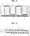
FIG. 3 is a top view illustrating the top surface of the wiring
board 2 with the TCP 1 mounted. FIG. 4 is a top view illustrating
the rear surface of the wiring board 2 with the TCP 1 mounted. FIG.
5 is a side view illustrating a short side of the wiring board 2
with the TCP 1 mounted.
The wiring board 2 made of a rectangular glass epoxy resin
sheet having a thickness of about 0.4 mm, a height (short side)
of about 25.4 mm, and a width (long side) of about 67.6 mm is mounted
on each of the top and rear surfaces thereof with four rows of the
TCPs 1 along the short and long sides of the wiring board 2, amount
to a total of 4 x 4 = 16 (32 on both surfaces). Each of these TCPs
1 encapsulates a semiconductor chip (not shown) formed with a
16-megabit (Mbit) DRAM (Dynamic Random Access Memory) for example.
Each TCP 1 is electrically connected to the wiring board 2 through
a plurality of leads 4 arranged in a row along one side of the TCP
1.
One of the long sides of the wiring board 2 provides a connector.
The connector is arranged on the top and rear sides thereof with
a plurality of terminals (connector pins) 5 in a row for inserting
this memory module into a socket of the mother board. Also, the
wiring board 2 is mounted in an excess area thereof with small
electronic parts 6 and 7 such as a chip capacitor and a clock
generator as required.
The 32 TCPs 1 mounted on the wiring board 2 are all of the
same dimensions. These TCPs 1 are all mounted at a small tilt angle
of about 8 degrees relative to the mounting surface. In this
mounting structure, the total thickness of the wiring board 2
including the TCPs 1 on both the sides is extremely small, complying
with the strict memory module specifications in height (a maximum
total height of 3.8 mm).
As shown in FIG. 5, of the four TCPs 1 arranged in a row along
the short side of the wiring board 2, the three TCPs 1 except the
TCP 1 at one end of the wiring board are mounted such that each
gets at one part thereof under the adjacent TCP 1. This mounting
structure allows the mounting of higher density than that the all
four TCPs 1 are mounted flat to the mounting surface. As described
above, each TCP 1 is mounted at a small tilt angle not more than
45 degrees, so that the surface area of each of these three TCPs
1 not covered by the adjacent TCP 1 increases, thereby enhancing
heat dissipation of the densely mounted TCPs 1.
As shown in FIG. 5, a slight gap S is provided in the overlapped
portion between adjacent TCPs 1 along the short direction of the
wiring board 2. That is, these TCPs 1 are mounted such that each
does not come in contact with the other. This mounting structure
facilitates the air convection in the gap between the adjacent TCPs
1 mounted in a tilted relation to the mounting surface of the wiring
board 2, further enhancing heat dissipation of the densely mounted
TCPs 1.
Referring to FIGS. 3 and 4, of the 16 TCPs 1 mounted on each
side of the wiring board 2, the TCPs 1 in the left-most row and
the third row from the left end of the wiring board are arranged
such that their leads 4 come to the top of the wiring board. On
the other hand, the TCPs 1 in the second and fourth rows from the
left end of the wiring board are arranged such that their leads
4 come to the bottom (the connector side) of the wiring board. In
other words, the four rows of TCPs 1 arranged along the long side
of the wiring board 2 are mounted such that each row alternates
180 degrees to the other in the mounting surface.
The above-mentioned mounting structure allows the wiring of
groups of wires for interconnecting the same pins of the two
adjacent rows of TCPs 1 along the long side of the wiring board
2 without intersecting the wiring groups within the same mounting
surface. Consequently, the number of wires to be laid from one
side of the wiring board 2 to the other by way of through-holes
is reduced as compared with the mounting in which the 16 TCPs 1
are arranged in the same direction. This arrangement in turn
reduces the number of through-holes and the length of wiring,
thereby realizing the high-density mounting of many TCPs 1 on the
wiring board 2 limited in mounting area.
As shown in FIG. 5, the TCP 1 mounted on one side of the wiring
board 2 and the TCP 1 mounted on the other side in an opposite manner
are arranged such that the leads 4 of these TCPs 1 are directed
in the opposite directions (to the left side and the right side
in the figure). In this mounting structure, the pins of the TCPs
1 which are opposed to each other with the wiring board 2 sandwiched
in are directed in the same direction. Consequently, the number
of wires to be laid from one side of the wiring board 2 to the other
by way of through-holes is reduced as compared with the mounting
structure in which the TCPs 1 mounted on both sides of the wiring
board 2 are directed in the same direction. This in turn reduces
the number of through-holes and the length of wiring, thereby
realizing the high-density mounting of many TCPs 1 on the wiring
board 2 limited in mounting area.
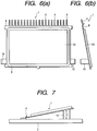
Referring to FIG. 6A (the top view of the TCP 1) and FIG. 6B
(the side view of the TCP 1), the TCP 1 has an insulating tape 8,
the plurality of leads 4 arranged on one side of the tape, a potting
resin 9 for encapsulating a semiconductor chip 13, and a pair of
support leads 10 arranged at two opposite short sides. As shown
in FIG. 7, support leads 10 function to hold the TCP 1 to a constant
tilt angle relative to the mounting surface of the wiring board
2. Varying distance (L) vertical to the mounting surface allows
the TCP 1 to be mounted at a desired tilt angle.
To fabricate the above-mentioned TCP 1, the insulating tape
8 formed with the leads 4 and the pair of support leads 10 on one
side is prepared at the outset. It should be noted that the
insulating tape 8, which is usually long, is shown only in its part
(for carrying only a single TCP).
The insulating tape 8 is formed by a polyimide resin for
example. The leads 4 and the pair of support leads 10 are formed
by etching a metal foil such as a rolled copper foil laminated on
one side of the insulating tape 8. One end (the tip of the inner
lead portion 4a) of each lead 4 extends into inside a device hole
12 in which the semiconductor chip is arranged. The base end
portion 4b of the outer lead portion 4c of each lead 4 is wider
than the other portion of the outer lead to prevent the potting
resin 9 from trailing (in the direction of the tip of the outer
lead 4c), reinforce the leads 4, and prevent the same from being
delaminated.
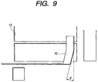
As shown in FIG. 9 in an expanded manner, the support lead
10 is bent halfway toward the short side by an angle () relative
to the long side of the TCP 1. Adjusting the bend angle () in
this portion determines the tilt angle () at which the TCP 1 is
mounted on the wiring board 2. In the present embodiment, this
bend angle () is set to about 8 degrees.
Next, a semiconductor chip 13 as shown in FIG. 10A is prepared.
The semiconductor chip 1 is formed on the main surface thereof with
a 16-megabit DRAM. A plurality of bonding pads 14 are also formed
on the main surface of the semiconductor chip 13 in the center area
of the chip along its long side. A gold (Au) bump electrode 14a
for electrically connecting the tip of the inner lead 4a to the
pad 14 is connected to each bonding pad 14 on the surface thereof
as shown in FIG. 14B.
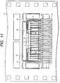
The semiconductor chip 13 is positioned inside the device hole
12 of the insulating tape 8 as shown in FIG. 11. Then, the bonding
pad 14 of the semiconductor chip 13 is electrically connected to
the corresponding inner lead portion 4a at one end portion through
the Au bump electrode 14a by use of a known inner lead bonder, not
shown.
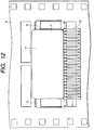
As shown in FIG. 12, the main surface side of the semiconductor
chip including the junction between bonding pad 14 of the
semiconductor chip 13 and the lead 4a is encapsulated with the
potting resin 9 of epoxy type.
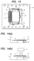
The outer lead portion 4c of each lead 4, the support lead
10, and a part of the insulating tape 8 are cut at the positions
indicated by thick lines (A to F) shown in FIG. 13, the support
lead 10 is bent at halfway thereof by 90 degrees, and the outer
lead portion 4c of the lead 4 is bent into the shape as shown in
FIG. 6B by use of a known cutting and forming die (not shown). Thus,
the TCP 1 is completed.
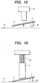
To mount the TCP 1 thus obtained on the wiring board 2, the
TCP 1 horizontally accommodated beforehand in a pocket 11a of a
tray 11 as shown in FIG. 14A is held by a vacuum nozzle 17 and placed
on a positioning stage 21 shown in FIG. 15. At this moment, the
tip of the vacuum nozzle 17 is constituted by a soft member such
as a rubber or soft resin for example and a load mitigating mechanism
for making this tip portion vertically movable by use of a spring
17a is provided on the vacuum nozzle 17. These provisions prevent
the lead 4 and the support lead 10 from being deformed by the weight
of the vacuum nozzle 17 when the TCP 1 is brought down into intimate
contact with the positioning stage 21 by the vacuum nozzle 17. In
addition, the vacuum nozzle 17 is provided at the bottom thereof
with a tilt of the same angle (about 8 degrees) as the tilt angle
of the TCP 1 as shown, allowing the TCP 1 to be vacuum-held with
the tilt angle kept unchanged.
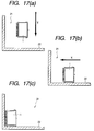
As shown in FIGS. 17A through 17C, the positioning stage on
which the TCP 1 is placed is moved in X and Y directions to position
the TCP 1 to the reference point of a square fixing jig 22. Then,
the TCP 1 is held by the vacuum nozzle 17 again to be carried to
a predetermined position on the wiring board 2 according to
predetermined positional information. As shown in FIG. 18, the
lead 4 of the TCP 1 is temporarily attached to a foot print 18 of
the wiring board 2 with solder paste printed beforehand. The
solder is reflowed with the tilt angle of the TCP 1 relative to
the mounting surface kept constant by the support lead 10 to solder
the lead 4 to the foot print 18.
At this moment, to prevent the reflowed solder from creeping
the lead 4 up to the base end portion 4b (refer to FIG. 8) thereof
to melt with the solder of an adjacent lead 4, namely to prevent
a so-called solder bridge failure from occurring, a bent 4d as shown
in the figure is provided halfway along the lead 4 to pool the solder,
thereby preventing the same from creeping up to the base end portion
4b. In addition, this bent 4d acts to mitigate or absorb a stress
applied to the lead 4 by means of the deformation of the bent,
thereby preventing the lead 4 from being broken.
When mounting the TCP 1 on the wiring board 2, the support
lead 10 is not fixed to the wiring board 2. By doing so, if the
TCP 1 mounted so that a part thereof gets under an adjacent TCP
1a fails after mounting, the adjacent TCP 1 may be lifted around
the junction between the wiring board 2 and the lead 4 as shown
in FIG. 20 to replace the failing TCP 1 with ease. Also, when
mounting the TCP 1 on the wring board 2, small electronic parts
(6, 7) such as the chip capacitor and an LSI package of planar
mounting type such as a CSP (Chip Size Package) are mounted as
required at the same time.
Then, when the wiring board 2 mounted with TCPs 1 is
accommodated in the case 3, the memory module shown in FIGS. 1 and
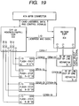
2 is completed. FIG. 19 is a circuit diagram of the memory module
practiced as the above-mentioned embodiment of the invention.
The case 3 for accommodating the wiring board 2 is formed by
punching a thin metal sheet having a high thermal conductivity such
as aluminum (Al), folding the resultant thin metal sheet into two
parts, and inserting the wiring board 2 between the these parts.
This structure prevents the TCPs 1 mounted on the wiring board 2
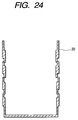
from being deformed. In doing so, a resin sheet shaped as shown
in FIG. 24 may be inserted between the TCPs 1 mounted on the wiring
board 2 as a spacer 20 as shown in FIGS. 22 and 23. This arrangement
enhances the mechanical strength of the memory module, thereby
preventing the TCPs 1 from being deformed by a strong force that
is applied to the case 3 when the memory module is inserted in the
socket of a mother board. The spacer 20 is fixed to the wiring
board 2 by means of an adhesive or mechanical insertion.
Preferred embodiment 2:
An electronic apparatus practiced as a second preferred
embodiment of the invention is a memory card for use as an external
auxiliary storage device for a note-size personal computer for
example.
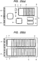
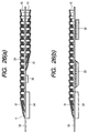
FIG. 25A is a top view illustrating the front side of a wiring
board to be accommodated in this memory card. FIG. 25B is a top
view illustrating the rear side of this wiring board. FIG. 26A
is a side view illustrating one long side of this wiring board.
FIG. 26B is a side view illustrating the other long side of the
wiring board. It should be noted that a case for accommodating
the wiring board is not shown.
Eight TCPs 31 are mounted in a row on the front surface of
the wiring board 30. On the rear surface of the wiring board 30,
32 TCPs 31 are mounted in two rows (a total of 40 TCPs 31 on both
sides). In each of the TCPs 32, a semiconductor chip (not shown)
formed with a 64-megabit (Mbit) flash memory for example is
encapsulated. Each TCP 31 is electrically connected to the wiring
board 30 through a plurality of leads 4 arranged in a row along
one side of the TCP 31.
The other portions of the front surface of the wiring board
30 are arranged with a decoder 32, a microcomputer 33, an interface
circuit 34, a TTL 35 for reset signal generation, and a clock module
36. The interface circuit 34 is of a chip-on-board (COB) structure
and can be constituted by a planar mount type package such as a
chip size package (CSP). One of the short sides of the wiring board
30 is a connector that is arranged on the front and rear sides
thereof with a plurality of terminals (connector pins) 37 in a row.
The 40 TCPs 31 mounted on the wiring board 2 are all of the
same dimensions. As shown in FIGS. 26A and 26B, each TCP 31 is
mounted with a small tilt angle to the mounting surface. The tilt
angle is adjustable by means of the support lead 10 in the same
manner as the TCP 1 of the first embodiment. Except for the TCP
31 arranged at one end of the wiring board, the TCPs 31 are mounted
such that a portion of each gets under the adjacent one. The
overlapped portion is provided a slight gap in between.
The above-mentioned mounting structure keeps extremely small
the thickness (or height) of the wiring board 30 mounted on both
sides with the TCPs 31, complying with the memory card standards
strict in height specification (a maximum of 5 mm). The
above-mentioned mounting structure also realizes the high-density
mounting of many TCPs 31 on the wiring board 30 limited in mounting
dimensions. The TCP 31 may be fabricated and mounted on the wiring
board 30 in generally the same manner as described with respect
to the above-mentioned preferred embodiment 1.
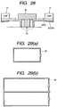
As shown in FIGS. 27A, 27B, and 28, spacers 38 and 39 as shown
in FIGS. 29A and 29B are inserted into a gap of the TCPs 31 to enhance
the mechanical strength of the memory card. The spacer 38 is
arranged around the 8 TCPs 31 mounted on the front surface of the
wiring board 30. The spacer 39 is arranged around the 32 TCPs 31
mounted on the rear surface of the wiring board 30.
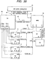
FIG. 30 is a circuit diagram illustrating the memory card of
the second embodiment fabricated as described above.
The memory card described with reference to FIGS. 25 through
29 constitutes an ATA (AT Attachment) card system shown in FIG.
30 for example. The ATA card complies with the interface and
protocol to be used by an AT-compatible computer for accessing a
hard disk drive. This card is standardized by the standardizing
organization of PCMCIA (Personal Computer Memory Card
International Association).
Reference numeral 40 denotes the pin connector of the ATA card
that corresponds to an external terminal 37. Through this external
terminal 37, the ATA card transfers signals with a PC (Personal
Computer) or a PDA (Personal Digital Assistant). The number of
external terminals and the names and numbers thereof are determined
by PCMCIA.
Externally supplied data and addresses are inputted in a gate
array GA 34 through a signal line 41. The gate array GA controls
an external PCMCIA interface, a microcomputer MPU 33, a flash memory
FM 31, and the data transfer between the flash memory FM 31 and
the PCMCIA interface. The transfer of data and addresses between
elements in the card is performed through a local data bus and a
local address bus referenced at 42.
The MPU 33 receives an externally supplied command 44 to
perform data control. Externally supplied data is sent to the
flash memory FM 31 through a decoder DC for high-speed data
processing for both read and write operations. Selection of the
flash memory FM 31 for data writing and data reading is controlled
by a CEN (Chip Enable) bus 43. Further, to enhance the reliability
of the data stored in the flash memory FM 31, the MPU 33 performs
ECC (Error Check and Correction) (for controlling the count of
rewriting of each section and controlling access to failing
sectors) and wear leveling (averaging the count of rewriting
failing sectors).
While the preferred embodiments of the present invention have
been described using specific terms, such description is for
illustrative purposes only, and it is to be understood that changes
and variations may be made without departing from the spirit or
scope of the appended claims.