EP0923153A1 - Chip-antenna - Google Patents
Chip-antenna Download PDFInfo
- Publication number
- EP0923153A1 EP0923153A1 EP98123650A EP98123650A EP0923153A1 EP 0923153 A1 EP0923153 A1 EP 0923153A1 EP 98123650 A EP98123650 A EP 98123650A EP 98123650 A EP98123650 A EP 98123650A EP 0923153 A1 EP0923153 A1 EP 0923153A1
- Authority
- EP
- European Patent Office
- Prior art keywords
- antenna
- conductor
- chip
- base member
- conductors
- Prior art date
- Legal status (The legal status is an assumption and is not a legal conclusion. Google has not performed a legal analysis and makes no representation as to the accuracy of the status listed.)
- Granted
Links
- 239000004020 conductor Substances 0.000 claims abstract description 147
- 239000000919 ceramic Substances 0.000 claims abstract description 7
- 230000005404 monopole Effects 0.000 description 9
- 239000000758 substrate Substances 0.000 description 9
- 230000003247 decreasing effect Effects 0.000 description 4
- 230000004048 modification Effects 0.000 description 4
- 238000012986 modification Methods 0.000 description 4
- 230000000694 effects Effects 0.000 description 3
- 238000003780 insertion Methods 0.000 description 3
- 230000037431 insertion Effects 0.000 description 3
- VYPSYNLAJGMNEJ-UHFFFAOYSA-N Silicium dioxide Chemical compound O=[Si]=O VYPSYNLAJGMNEJ-UHFFFAOYSA-N 0.000 description 2
- QVQLCTNNEUAWMS-UHFFFAOYSA-N barium oxide Chemical compound [Ba]=O QVQLCTNNEUAWMS-UHFFFAOYSA-N 0.000 description 2
- 238000010030 laminating Methods 0.000 description 2
- ORQBXQOJMQIAOY-UHFFFAOYSA-N nobelium Chemical compound [No] ORQBXQOJMQIAOY-UHFFFAOYSA-N 0.000 description 2
- 239000007787 solid Substances 0.000 description 2
- RYGMFSIKBFXOCR-UHFFFAOYSA-N Copper Chemical compound [Cu] RYGMFSIKBFXOCR-UHFFFAOYSA-N 0.000 description 1
- 229910000881 Cu alloy Inorganic materials 0.000 description 1
- 229910052802 copper Inorganic materials 0.000 description 1
- 239000010949 copper Substances 0.000 description 1
- 230000008020 evaporation Effects 0.000 description 1
- 238000001704 evaporation Methods 0.000 description 1
- 238000004519 manufacturing process Methods 0.000 description 1
- 238000000034 method Methods 0.000 description 1
- TWNQGVIAIRXVLR-UHFFFAOYSA-N oxo(oxoalumanyloxy)alumane Chemical compound O=[Al]O[Al]=O TWNQGVIAIRXVLR-UHFFFAOYSA-N 0.000 description 1
- 230000035699 permeability Effects 0.000 description 1
- 238000007747 plating Methods 0.000 description 1
- 238000007639 printing Methods 0.000 description 1
- 238000007650 screen-printing Methods 0.000 description 1
- 239000000377 silicon dioxide Substances 0.000 description 1
- 238000005245 sintering Methods 0.000 description 1
Images




Classifications
-
- H—ELECTRICITY
- H01—ELECTRIC ELEMENTS
- H01Q—ANTENNAS, i.e. RADIO AERIALS
- H01Q1/00—Details of, or arrangements associated with, antennas
- H01Q1/36—Structural form of radiating elements, e.g. cone, spiral, umbrella; Particular materials used therewith
- H01Q1/38—Structural form of radiating elements, e.g. cone, spiral, umbrella; Particular materials used therewith formed by a conductive layer on an insulating support
-
- H—ELECTRICITY
- H01—ELECTRIC ELEMENTS
- H01Q—ANTENNAS, i.e. RADIO AERIALS
- H01Q1/00—Details of, or arrangements associated with, antennas
- H01Q1/36—Structural form of radiating elements, e.g. cone, spiral, umbrella; Particular materials used therewith
- H01Q1/362—Structural form of radiating elements, e.g. cone, spiral, umbrella; Particular materials used therewith for broadside radiating helical antennas
Definitions
- the present invention relates to a chip-antenna. More particularly, the present invention relates to a chip-antenna for use in a low-frequency band radio equipment such as a television, a radio, a pager, for example.
- a low-frequency band radio equipment such as a television, a radio, a pager, for example.
- a monopole antenna 100 as a representative wire antenna is shown.
- the dimensions of the radiating element of the antenna become large.
- the wavelength in the air is ⁇
- a radiating element having a length of ⁇ /4 is required and then the length of the radiating element of a monopole antenna becomes as long as about 40 mm for a 1.9 GHz band.
- the bandwidth of a monopole antenna having a reflection loss of less than - 6 (dBd) is as narrow as about 30 MHz. Accordingly, there has been a problem that it is difficult to use the monopole antenna in the cases where a small-sized and wide-band antenna is needed.
- Preferred embodiments of the present invention are provided to overcome the above described problems, and provide a small-sized chip-antenna to be able to be used for a wide-band radio equipment.
- a preferred embodiment of the present invention provides a chip-antenna, comprising: a base member including a mounting surface and made of at least one of dielectric ceramic and magnetic ceramic; at least two conductors disposed within said base member or on a surface of said base member, at least a portion of said conductors being substantially perpendicular to the mounting surface of said base member; a feeding electrode for applying a voltage to said conductors and disposed on the surface of said base member; a ground electrode disposed at least one on the surface of and within said base member; one of said conductors being served as a first conductor, one end of which is connected to said feeding electrode; the rest of said conductor being served as a second conductor, one end of which are connected to said ground electrode; and the other end of said first conductor and the other end of said second conductor being connected.
- the first conductor and the second conductor are connected in series between the feeding electrode and the ground electrode respectively disposed on the surface of the base member, a capacitance is able to be given between the ground on the mounting substrate where the chip-antenna is mounted and the vicinity of the connecting portion of the other end of the first conductor and the other end of the second conductor.
- the capacitance component C is able to be increased without changing the inductance component L and the resistance component R of the first conductor and the second conductor.
- the bandwidth of the chip-antenna becomes widened, and accordingly it becomes possible to widen the bandwidth of a small-sized chip-antenna even if its height is less than one tenth of a conventional monopole antenna.
- a radio equipment mounted with such a chip-antenna and requiring frequencies of a wide band is able to be small-sized.
- a capacitance loading conductor may be disposed at least one on the surface of or within said base member, and the other end of said first conductor and the other end of said second conductor are connected via said capacitance loading conductor.
- the first conductor and the second conductor are connected in series via the capacitance loading conductor between the feeding electrode and the ground electrode respectively disposed on the surface of the base member, a capacitance given between the capacitance loading conductor and the ground on the mounting substrate where the chip-antenna is mounted is able to be controlled by choosing the area of the capacitance loading conductor. As the result, the input impedance of the chip-antenna can be controlled.
- the input impedance of the chip-antenna is able to be made in agreement with the characteristic impedance of the high-frequency portion of a radio equipment with the chip-antenna mounted, and any matching circuits become unnecessary.
- a radio equipment with the chip-antenna mounted is realized to be of small size.
- a gap portion may be provided in said base member between said first conductor and second conductor.
- the relative dielectric constant of the base member is able to be adjusted by adjusting the size of the gap portion, and thereby the value of a capacitance given between the ground on the mounting substrate where the chip-antenna is mounted and the vicinity of the connecting portion of the other end of the first conductor and the other end of the second conductor can be adjusted. Therefore, the input impedance of a chip-antenna can be more precisely matched to the characteristic impedance of a radio equipment with a chip-antenna to be mounted. Further, by forming a gap portion in a base member, the base member becomes light-weighted and accordingly the weight of a chip-antenna is made light.
- said first and second conductors may be wound in substantially spiral shape.
- the line length of the first and second conductors is able to be lengthened, and the current distribution can be increased. Accordingly, the gain of the chip-antenna can be improved.
- said first and second conductors may be wound in substantially helical shape.
- the line length of the first and second conductors is also able to be lengthened, and the current distribution can be increased. Accordingly, the gain of the chip-antenna can be improved.
- Fig. 1 is a perspective view of a chip-antenna according to a first preferred embodiment of the present invention.
- Fig. 2 is an exploded perspective view of the chip-antenna in Fig. 1.
- Fig. 3 shows the frequency characteristic of insertion loss of the chip-antenna in Fig. 1.
- Fig. 4 is a perspective view of a modification of the chip-antenna in Fig. 1.
- Fig. 5 is a perspective view of a chip-antenna according to a second preferred embodiment of the present invention.
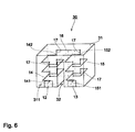
- Fig. 6 is a perspective view of a chip-antenna according to a third embodiment of the present invention.
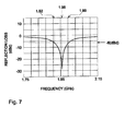
- Fig. 7 shows the frequency characteristic of insertion loss of the chip-antenna in Fig. 6.
- Fig. 8 is a perspective view of a modification of the chip-antenna in Fig. 6.
- Fig. 9 is a perspective view of a chip-antenna according to a fourth embodiment of the present invention.
- Fig. 10 shows the frequency characteristic of insertion loss of the chip-antenna in Fig. 9.
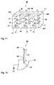
- Fig. 11 is a perspective view of a chip-antenna according to a fifth preferred embodiment of the present invention.
- Fig. 12 shows a conventional monopole antenna.
- the chip-antenna 10 comprises a base member 11 of a rectangular solid having a mounting surface 111 and a feeding electrode 12 and a ground electrode 13 are disposed on the surface of the base member 11.
- a first conductor 14 with one end 141 connected to the feeding electrode 12 and a second conductor 15 with one end 151 connected to the ground electrode 13, both of which are spirally wound and the spiral axis thereof are perpendicular to the mounting surface 111 of the base member 11 i.e., in the direction of height of the base member 11 are disposed within the base member 11.
- the other end 142 of the first conductor 14 and the other end 152 of the second conductor 15 are connected via a connecting line 16. Accordingly, the first conductor 14 and the second conductor 15 come to have been connected in series between the feeding electrode 12 and the ground electrode 13 disposed on the surface of the base member 11.
- the external dimensions of the chip-antenna are, for example, of a measure of 10.0 mm (L) x 6.3 mm (W) x 5.0 mm (H).
- the base member 11 is formed by laminating rectangular thin layers la through lg made of dielectric ceramics, the main components of which are barium oxide, aluminum oxide, and silica.
- conductor patterns 4a through 4e, 5a through 5e having substantially an U-shaped form and a connecting line 16 having substantially a linear shape of copper or copper alloy are provided by printing, evaporation, pasting, or plating.
- via holes 17 are provided at a predetermined position of thin layers 1b through 1f (one end of conductor patterns 4b through 4e, 5b through 5e and both ends of a connecting line 16) in the thickness direction.
- one end of the first conductor 14 (one end of the conductor pattern 4a) is led out to one surface of the base member 11 and connected the feeding electrode 12 disposed on the surface of the base member 11 in order to apply a voltage to the first and second conductors 14, 15.
- one end of the second conductor 15 (one end of the conductor pattern 5a) is led out on the surface of the base member 11 and connected to the ground electrode 13 disposed on the surface of the base member 11 in order to be connected to the ground (not illustrated) on a mounting substrate for the chip-antenna 10 to be mounted.
- the line length of the first and second conductors 14, 15 is able to be lengthened and accordingly the distribution of current is able to be increased. Therefore, the gain of the chip-antenna 10 can be improved.
- Fig. 3 the frequency characteristic of the reflection loss of the chip-antenna (Fig. 1) is shown. From this drawing, it is understood that the bandwidth in which a reflection loss is of less than - 6 (dBd) in reference to the central frequency of 1.94 GHz is about 70 MHz, that is, a wider bandwidth has been attained.
- a perspective view of a modification of the chip-antenna in Fig. 1 is shown.
- a base member 11a of a rectangular solid, a feeding electrode 12a and a ground electrode 13a disposed on the surface of the base member 11a, and first and second conductors 14a, 15a meanderingly formed within the base member 11a are given.
- one end 141a of the first conductor 14a is connected to a feeding electrode 12a and one end 151a of the second conductor 15a is connected to a ground electrode 13a respectively.
- the other end 142a of the first conductor 14a and the other end 152a of the second conductor 15a are connected.
- the line length of the first and second conductors 14a, 15a is able to be lengthened and accordingly the distribution of current is able to be increased. Therefore, the gain of the chip-antenna 10a can be improved.
- the first and second conductors 14a, 15a of a meandering form may be formed on the surface (one main surface) of the base member 11a.
- a capacitance is able to be given, and without changing the inductance components and resistance components of the first conductor and second conductor it is possible to increase only the capacitance component.
- the bandwidth of the chip-antenna is widened and then it becomes possible to widen the bandwidth of a small-sized chip-antenna even if its height is less than one tenth of a conventional monopole antenna.
- a radio equipment mounted with such a chip-antenna and requiring frequencies of a wide band is able to be made of small size.
- FIG. 5 an exploded perspective view of a second embodiment of a chip-antenna according to the present invention is shown.
- the chip-antenna 20 is different from the chip-antenna 10 of the first preferred embodiment in that the other end 142 of a first conductor 14 and the other end 152 of a second conductor 15 are connected to a capacitance loading conductor 21 disposed within the base member 11 through via holes 17.
- the first conductor 14 and second conductor 15 come to have been connected in series between a feeding electrode 12 and a ground electrode 13 disposed on the surface of the base member 11 through the capacitance loading conductor 21.
- the chip-antenna of the second preferred embodiment because between the feeding electrode and the ground electrode disposed on the surface of the base member the first conductor and second conductor are connected in series through the capacitance loading conductor, by choosing the area of the capacitance loading conductor a capacitance given between the capacitance loading conductor and the ground on the mounting substrate for the chip-antenna to be mounted is able to be controlled. As the result, the input impedance to the chip-antenna can be controlled.
- the input impedance of a chip-antenna is able to be made in agreement with the characteristic impedance of the high-frequency portion of a radio equipment with a chip-antenna mounted, and any matching circuit becomes unnecessary. As the result, a radio equipment of small size is realized.
- Fig. 6 shows a perspective view of a third preferred embodiment of a chip-antenna according to the present invention.
- the chip-antenna 30 is different from the chip-antenna 10 of the first preferred embodiment in that a base member 31 has a gap portion 32 between a first conductor 14 and a second conductor 15.
- Fig. 7 shows the frequency characteristic of reflection loss of the chip-antenna 30 shown in Fig. 6. From this drawing, it is understood that the bandwidth in which a reflection loss is of less than - 6 (dBd) in reference to the central frequency of 1.96 GHz is about 70 MHz, that is, a wider bandwidth has been attained.
- Fig. 8 shows a perspective view of a modification of the chip-antenna 30 in Fig. 6.
- a base member 31a having a rectangular shape, a feeding electrode 12a and a ground electrode 13a disposed on the surface of the base member 31a, and first and second conductors 14a, 15a spirally wound in the direction of height of the base member 31a along the surface of the base member 11a are given.
- one end 141a of the first conductor 14a is connected to a feeding electrode 12a and one end 151a of the second conductor 15a is connected to a ground electrode 13a respectively.
- the other end 142a of the first conductor 14a and the other end 152a of the second conductor 15a are connected through a connecting line 16a.
- the manufacturing processes of the chip-antenna 10a can be made simple.
- the gap portion is given to the base member and accordingly by adjusting the size of the gap portion the relative dielectric constant of the base member is able to be adjusted, the value of a capacitance given between the vicinity of the connecting portion of the other end of the first conductor and the other end of the second conductor and the ground on the mounting substrate where the chip-antenna is mounted can be adjusted. Therefore, the input impedance of the chip-antenna can be more precisely matched to the characteristic impedance of the radio equipment with a chip-antenna to be mounted.
- the base member becomes light-weighted and accordingly the weight of the chip-antenna is made light.
- Fig. 9 shows an exploded perspective view of a fourth preferred embodiment of a chip-antenna according to the present invention.
- the chip-antenna 40 is different from the chip-antenna of the third preferred embodiment in that the other end 142 of a first conductor 14 and the other end 152 of a second conductor 15 are connected to a capacitance loading conductor 21 provided within the base member 31 through via holes 17.
- the first conductor 14 and the second conductor 15 come to have been connected in series between a feeding electrode 12 and a ground 13 disposed on the surface of the base member 31 via the capacitance loading conductor 21.
- Fig. 10 shows the frequency characteristic of reflection loss of the chip-antenna 40 (Fig. 9). From this drawing, it is understood that the bandwidth in which a reflection loss of less than - 6 (dBd) in reference to the central frequency of 1.96 GHz is about 90 MHz and when compared with the chip-antenna 30 of the third embodiment a wider bandwidth has been attained.
- Fig. 11 shows a perspective view of a fifth preferred embodiment of a chip-antenna according to the present invention.
- the chip-antenna 50 is different from the chip-antenna of the first preferred embodiment in that a first conductor 14 with one end 141 connected to a feeding electrode 12 and two second electrodes 51, 52 with one ends 511, 512 connected to a ground electrode 13 are given and the other end 142 of the first conductor 14 and the other ends 512, 522 of the second conductors 51, 52 are connected via a connecting line 53.
- the first conductor 14 and one second conductor 51, and the first conductor 14 and the other second conductor 52 come to have been connected in series between the feeding electrode 12 and the ground electrode 13 disposed on the surface of the base member 11 via the connecting line 53 disposed within the base member 11.
- the chip-antenna of the fifth preferred embodiment because between the feeding electrode and the ground electrode the first conductor and one of the second conductors and the first conductor and the other of the second conductors are connected in series respectively, by adjusting the ratio of the number of turns of the first conductor to that of the second conductors and the ratio of the number of turns of the first conductor to that of the other of the second conductors, the input impedance of the chip-antenna is able to be fine-adjusted. Accordingly, it becomes possible to adjust the input impedance of the chip-antenna to the characteristic impedance of a radio equipment which is mounted with the chip-antenna.
- the chip-antenna is able to have two resonance frequencies. As the result, a wider bandwidth can be realized.
- three or more second conductors may be given.
- the input impedance of the chip-antenna can be more accurately fine-adjusted. Therefore, it becomes possible to adjust the chip-antenna more precisely to the characteristic impedance of the high-frequency portion of a radio equipment mounted with the chip-antenna.
Landscapes
- Details Of Aerials (AREA)
Abstract
Description
- The present invention relates to a chip-antenna. More particularly, the present invention relates to a chip-antenna for use in a low-frequency band radio equipment such as a television, a radio, a pager, for example.
- In Fig. 12, a
monopole antenna 100 as a representative wire antenna is shown. Thismonopole antenna 100 has aradiating element 102 set up substantially perpendicular to thegrounding surface 101 in air (dielectric constant ε = 1, relative magnetic permeability µ = 1). And, a feeding power supply V is connected to oneend 103 of thisradiating element 102, and theother end 104 is kept open. - However, in the case of the above-mentioned conventional monopole antenna, as the radiating element of the antenna is placed in the air, the dimensions of the radiating element of the antenna become large. For example, assuming that the wavelength in the air is λ, a radiating element having a length of λ/4 is required and then the length of the radiating element of a monopole antenna becomes as long as about 40 mm for a 1.9 GHz band. Further, the bandwidth of a monopole antenna having a reflection loss of less than - 6 (dBd) is as narrow as about 30 MHz. Accordingly, there has been a problem that it is difficult to use the monopole antenna in the cases where a small-sized and wide-band antenna is needed.
- Preferred embodiments of the present invention are provided to overcome the above described problems, and provide a small-sized chip-antenna to be able to be used for a wide-band radio equipment.
- A preferred embodiment of the present invention provides a chip-antenna, comprising: a base member including a mounting surface and made of at least one of dielectric ceramic and magnetic ceramic; at least two conductors disposed within said base member or on a surface of said base member, at least a portion of said conductors being substantially perpendicular to the mounting surface of said base member; a feeding electrode for applying a voltage to said conductors and disposed on the surface of said base member; a ground electrode disposed at least one on the surface of and within said base member; one of said conductors being served as a first conductor, one end of which is connected to said feeding electrode; the rest of said conductor being served as a second conductor, one end of which are connected to said ground electrode; and the other end of said first conductor and the other end of said second conductor being connected.
- According to the above described chip-antenna, because the first conductor and the second conductor are connected in series between the feeding electrode and the ground electrode respectively disposed on the surface of the base member, a capacitance is able to be given between the ground on the mounting substrate where the chip-antenna is mounted and the vicinity of the connecting portion of the other end of the first conductor and the other end of the second conductor. As a result, only the capacitance component C is able to be increased without changing the inductance component L and the resistance component R of the first conductor and the second conductor.
- Therefore, because the value of Q ( = (L/C)1/2/R ) of the chip-antenna is able to be decreased, the bandwidth of the chip-antenna becomes widened, and accordingly it becomes possible to widen the bandwidth of a small-sized chip-antenna even if its height is less than one tenth of a conventional monopole antenna. As the result, a radio equipment mounted with such a chip-antenna and requiring frequencies of a wide band is able to be small-sized.
- In the above described chip-antenna, a capacitance loading conductor may be disposed at least one on the surface of or within said base member, and the other end of said first conductor and the other end of said second conductor are connected via said capacitance loading conductor.
- According to the above structure, because the first conductor and the second conductor are connected in series via the capacitance loading conductor between the feeding electrode and the ground electrode respectively disposed on the surface of the base member, a capacitance given between the capacitance loading conductor and the ground on the mounting substrate where the chip-antenna is mounted is able to be controlled by choosing the area of the capacitance loading conductor. As the result, the input impedance of the chip-antenna can be controlled.
- Accordingly, by optimizing the area of the capacitance loading conductor the input impedance of the chip-antenna is able to be made in agreement with the characteristic impedance of the high-frequency portion of a radio equipment with the chip-antenna mounted, and any matching circuits become unnecessary. As the result, a radio equipment with the chip-antenna mounted is realized to be of small size.
- In the above described chip-antenna, a gap portion may be provided in said base member between said first conductor and second conductor.
- According to the above structure, the relative dielectric constant of the base member is able to be adjusted by adjusting the size of the gap portion, and thereby the value of a capacitance given between the ground on the mounting substrate where the chip-antenna is mounted and the vicinity of the connecting portion of the other end of the first conductor and the other end of the second conductor can be adjusted. Therefore, the input impedance of a chip-antenna can be more precisely matched to the characteristic impedance of a radio equipment with a chip-antenna to be mounted. Further, by forming a gap portion in a base member, the base member becomes light-weighted and accordingly the weight of a chip-antenna is made light.
- In the above described chip-antenna, said first and second conductors may be wound in substantially spiral shape.
- According to the above structure, the line length of the first and second conductors is able to be lengthened, and the current distribution can be increased. Accordingly, the gain of the chip-antenna can be improved.
- In the above described chip-antenna, said first and second conductors may be wound in substantially helical shape.
- According to the above structure, the line length of the first and second conductors is also able to be lengthened, and the current distribution can be increased. Accordingly, the gain of the chip-antenna can be improved.
- Other features and advantages of the present invention will become apparent from the following description of the invention which refers to the accompanying drawings.
- Fig. 1 is a perspective view of a chip-antenna according to a first preferred embodiment of the present invention.
- Fig. 2 is an exploded perspective view of the chip-antenna in Fig. 1.
- Fig. 3 shows the frequency characteristic of insertion loss of the chip-antenna in Fig. 1.
- Fig. 4 is a perspective view of a modification of the chip-antenna in Fig. 1.
- Fig. 5 is a perspective view of a chip-antenna according to a second preferred embodiment of the present invention.
- Fig. 6 is a perspective view of a chip-antenna according to a third embodiment of the present invention.
- Fig. 7 shows the frequency characteristic of insertion loss of the chip-antenna in Fig. 6.
- Fig. 8 is a perspective view of a modification of the chip-antenna in Fig. 6.
- Fig. 9 is a perspective view of a chip-antenna according to a fourth embodiment of the present invention.
- Fig. 10 shows the frequency characteristic of insertion loss of the chip-antenna in Fig. 9.
- Fig. 11 is a perspective view of a chip-antenna according to a fifth preferred embodiment of the present invention.
- Fig. 12 shows a conventional monopole antenna.
- In Figs. 1 and 2, a perspective view and an exploded perspective view of a first preferred embodiment of a chip-antenna according to the present invention are shown. The chip-
antenna 10 comprises abase member 11 of a rectangular solid having amounting surface 111 and afeeding electrode 12 and aground electrode 13 are disposed on the surface of thebase member 11. - Further, a
first conductor 14 with oneend 141 connected to thefeeding electrode 12 and asecond conductor 15 with oneend 151 connected to theground electrode 13, both of which are spirally wound and the spiral axis thereof are perpendicular to themounting surface 111 of thebase member 11 i.e., in the direction of height of thebase member 11 are disposed within thebase member 11. In this case, theother end 142 of thefirst conductor 14 and theother end 152 of thesecond conductor 15 are connected via a connectingline 16. Accordingly, thefirst conductor 14 and thesecond conductor 15 come to have been connected in series between thefeeding electrode 12 and theground electrode 13 disposed on the surface of thebase member 11.
In this embodiment, the external dimensions of the chip-antenna are, for example, of a measure of 10.0 mm (L) x 6.3 mm (W) x 5.0 mm (H).
And, thebase member 11 is formed by laminating rectangular thin layers la through lg made of dielectric ceramics, the main components of which are barium oxide, aluminum oxide, and silica. - On the surface of
thin layers 1a through 1f out of these,conductor patterns 4a through 4e, 5a through 5e having substantially an U-shaped form and a connectingline 16 having substantially a linear shape of copper or copper alloy are provided by printing, evaporation, pasting, or plating. - Further, via
holes 17 are provided at a predetermined position ofthin layers 1b through 1f (one end ofconductor patterns 4b through 4e, 5b through 5e and both ends of a connecting line 16) in the thickness direction. - And by the processes of laminating and sintering thin layers la through 1g, connecting
conductor patterns 4a through 4e, 5a through 5e through viaholes 17, and connecting the conductor pattern 4e andconductor pattern 5e by way of a connectingline 16 and viaholes 17, thefirst conductor 14 andsecond conductor 15 which are spirally wound in the direction of height of thebase member 11 and the other ends of which are connected together, are formed within thebase member 11. - In this case, one end of the first conductor 14 (one end of the
conductor pattern 4a) is led out to one surface of thebase member 11 and connected thefeeding electrode 12 disposed on the surface of thebase member 11 in order to apply a voltage to the first andsecond conductors conductor pattern 5a) is led out on the surface of thebase member 11 and connected to theground electrode 13 disposed on the surface of thebase member 11 in order to be connected to the ground (not illustrated) on a mounting substrate for the chip-antenna 10 to be mounted. - In the chip-
antenna 10 constructed this way, as the first andsecond conductors base member 11, the line length of the first andsecond conductors antenna 10 can be improved. - In Fig. 3, the frequency characteristic of the reflection loss of the chip-antenna (Fig. 1) is shown. From this drawing, it is understood that the bandwidth in which a reflection loss is of less than - 6 (dBd) in reference to the central frequency of 1.94 GHz is about 70 MHz, that is, a wider bandwidth has been attained.
- In Fig. 4, a perspective view of a modification of the chip-antenna in Fig. 1 is shown. In the chip-
antenna 10a, abase member 11a of a rectangular solid, a feedingelectrode 12a and aground electrode 13a disposed on the surface of thebase member 11a, and first andsecond conductors base member 11a are given. At this time, on the surface of thebase member 11a, oneend 141a of thefirst conductor 14a is connected to afeeding electrode 12a and oneend 151a of thesecond conductor 15a is connected to aground electrode 13a respectively. Further, within thebase member 11a, theother end 142a of thefirst conductor 14a and theother end 152a of thesecond conductor 15a are connected. In the chip-antenna 10a constructed this way, as the first andsecond conductors base member 11a, the line length of the first andsecond conductors antenna 10a can be improved. Further, the first andsecond conductors base member 11a. - As described above, according to a chip-antenna of the first preferred embodiment, because the first conductor and the second conductor are connected in series between a feeding electrode and a ground electrode disposed on the surface of a base member, between the vicinity of a connection portion of the other end of the first conductor and the other end of the second conductor, that is, the connecting line and the ground on the mounting substrate on which a chip-antenna is mounted a capacitance is able to be given, and without changing the inductance components and resistance components of the first conductor and second conductor it is possible to increase only the capacitance component. Accordingly, because the value of Q ( = (L/C)1/2/R ) of the chip-antenna is able to be decreased, the bandwidth of the chip-antenna is widened and then it becomes possible to widen the bandwidth of a small-sized chip-antenna even if its height is less than one tenth of a conventional monopole antenna. As the result, a radio equipment mounted with such a chip-antenna and requiring frequencies of a wide band is able to be made of small size.
- In Fig. 5, an exploded perspective view of a second embodiment of a chip-antenna according to the present invention is shown. The chip-
antenna 20 is different from the chip-antenna 10 of the first preferred embodiment in that theother end 142 of afirst conductor 14 and theother end 152 of asecond conductor 15 are connected to acapacitance loading conductor 21 disposed within thebase member 11 through via holes 17. - Accordingly, the
first conductor 14 andsecond conductor 15 come to have been connected in series between a feedingelectrode 12 and aground electrode 13 disposed on the surface of thebase member 11 through thecapacitance loading conductor 21. - As described above, according to the chip-antenna of the second preferred embodiment, because between the feeding electrode and the ground electrode disposed on the surface of the base member the first conductor and second conductor are connected in series through the capacitance loading conductor, by choosing the area of the capacitance loading conductor a capacitance given between the capacitance loading conductor and the ground on the mounting substrate for the chip-antenna to be mounted is able to be controlled. As the result, the input impedance to the chip-antenna can be controlled.
- Therefore, by optimizing the area of a capacitance feeding conductor the input impedance of a chip-antenna is able to be made in agreement with the characteristic impedance of the high-frequency portion of a radio equipment with a chip-antenna mounted, and any matching circuit becomes unnecessary. As the result, a radio equipment of small size is realized.
- More, between a capacitance loading conductor and a ground on the mounting substrate for a chip-antenna to be mounted on, a larger capacitance is able to be given. Accordingly, because the value of Q ( = (L/C)1/2/R ) of the chip-antenna is able to be decreased, the bandwidth of the chip-antenna can be made wider.
- More, even if a
capacitance loading conductor 21 is disposed on the surface of thebase member 11, the same effect can be obtained. - Fig. 6 shows a perspective view of a third preferred embodiment of a chip-antenna according to the present invention. The chip-
antenna 30 is different from the chip-antenna 10 of the first preferred embodiment in that abase member 31 has agap portion 32 between afirst conductor 14 and asecond conductor 15. - Fig. 7 shows the frequency characteristic of reflection loss of the chip-
antenna 30 shown in Fig. 6. From this drawing, it is understood that the bandwidth in which a reflection loss is of less than - 6 (dBd) in reference to the central frequency of 1.96 GHz is about 70 MHz, that is, a wider bandwidth has been attained. - Fig. 8 shows a perspective view of a modification of the chip-
antenna 30 in Fig. 6. In the chip-antenna 30a shown in Fig. 8, abase member 31a having a rectangular shape, a feedingelectrode 12a and aground electrode 13a disposed on the surface of thebase member 31a, and first andsecond conductors base member 31a along the surface of thebase member 11a are given. At this time, on the surface of thebase member 31a, oneend 141a of thefirst conductor 14a is connected to afeeding electrode 12a and oneend 151a of thesecond conductor 15a is connected to aground electrode 13a respectively. Further, on the surface of thebase member 31a, theother end 142a of thefirst conductor 14a and theother end 152a of thesecond conductor 15a are connected through a connectingline 16a. In the chip-antenna 30a constructed this way, as the first andsecond conductors base member 31a by screen printing, etc., the manufacturing processes of the chip-antenna 10a can be made simple. - As described above, according to the chip-antenna of the third preferred embodiment, because the gap portion is given to the base member and accordingly by adjusting the size of the gap portion the relative dielectric constant of the base member is able to be adjusted, the value of a capacitance given between the vicinity of the connecting portion of the other end of the first conductor and the other end of the second conductor and the ground on the mounting substrate where the chip-antenna is mounted can be adjusted. Therefore, the input impedance of the chip-antenna can be more precisely matched to the characteristic impedance of the radio equipment with a chip-antenna to be mounted.
- Further, by providing a gap portion in the base member, the base member becomes light-weighted and accordingly the weight of the chip-antenna is made light.
- Fig. 9 shows an exploded perspective view of a fourth preferred embodiment of a chip-antenna according to the present invention. The chip-
antenna 40 is different from the chip-antenna of the third preferred embodiment in that theother end 142 of afirst conductor 14 and theother end 152 of asecond conductor 15 are connected to acapacitance loading conductor 21 provided within thebase member 31 through via holes 17. - Therefore, in the same way as the chip-
antenna 20 of the second preferred embodiment thefirst conductor 14 and thesecond conductor 15 come to have been connected in series between a feedingelectrode 12 and aground 13 disposed on the surface of thebase member 31 via thecapacitance loading conductor 21. - Fig. 10 shows the frequency characteristic of reflection loss of the chip-antenna 40 (Fig. 9). From this drawing, it is understood that the bandwidth in which a reflection loss of less than - 6 (dBd) in reference to the central frequency of 1.96 GHz is about 90 MHz and when compared with the chip-
antenna 30 of the third embodiment a wider bandwidth has been attained. - As described above, according to the chip-antenna of the fourth preferred embodiment, between the capacitance loading conductor and the ground on the mounting substrate where the chip-antenna is to be mounted a larger capacitance is given. Accordingly, because the value of Q ( = (L/C)1/2/R ) of the chip-antenna is able to be decreased, the bandwidth of the chip-antenna can be made wider.
- Fig. 11 shows a perspective view of a fifth preferred embodiment of a chip-antenna according to the present invention. The chip-
antenna 50 is different from the chip-antenna of the first preferred embodiment in that afirst conductor 14 with oneend 141 connected to a feedingelectrode 12 and twosecond electrodes ground electrode 13 are given and theother end 142 of thefirst conductor 14 and the other ends 512, 522 of thesecond conductors line 53. - Therefore, the
first conductor 14 and onesecond conductor 51, and thefirst conductor 14 and the othersecond conductor 52 come to have been connected in series between the feedingelectrode 12 and theground electrode 13 disposed on the surface of thebase member 11 via the connectingline 53 disposed within thebase member 11. - As described above, according to the chip-antenna of the fifth preferred embodiment, because between the feeding electrode and the ground electrode the first conductor and one of the second conductors and the first conductor and the other of the second conductors are connected in series respectively, by adjusting the ratio of the number of turns of the first conductor to that of the second conductors and the ratio of the number of turns of the first conductor to that of the other of the second conductors, the input impedance of the chip-antenna is able to be fine-adjusted. Accordingly, it becomes possible to adjust the input impedance of the chip-antenna to the characteristic impedance of a radio equipment which is mounted with the chip-antenna.
- Further, because two second conductors are used, the chip-antenna is able to have two resonance frequencies. As the result, a wider bandwidth can be realized.
- Furthermore, in the above-mentioned second and third preferred embodiments, the cases in which the gap portion is given from substantially the central portion to the mounting surface of the base member are explained, but even if the gap portion is given from substantially the central portion to the surface opposite to the mounting surface of the base member or even if the gap portion is given like a cavity substantially at the central portion of the base member, the same effect can be obtained.
- More, in the above-mentioned fifth preferred embodiment, the cases in which the other end of the first conductor and the other ends of a plurality of second conductors are connected via the connecting line were explained, but like the third preferred embodiment the same effect can be obtained even if the other end of the first conductor and the other ends of a plurality of second conductors are connected via the capacitance loading conductor.
- More, three or more second conductors may be given. In this case, when the number of second conductors is increased, the input impedance of the chip-antenna can be more accurately fine-adjusted. Therefore, it becomes possible to adjust the chip-antenna more precisely to the characteristic impedance of the high-frequency portion of a radio equipment mounted with the chip-antenna.
- While the invention has been particularly shown and described with reference to preferred embodiments thereof, it will be understood by those skilled in the art that the forgoing and other changes in form and details may be made therein without departing from the spirit of the invention.
Claims (5)
- A chip-antenna (10; 10a; 20; 30; 40; 50) , comprising:a base member (11; 11a; 31) including a mounting surface (111) and made of at least one of dielectric ceramic and magnetic ceramic;at least two conductors (14, 15; 14a, 15a; 14, 51, 52) disposed within said base member (11; 11a; 31) or on a surface of said base member (11; 11a; 31), at least a portion of said conductors (14, 15; 14a, 15a; 14, 51, 52) being substantially perpendicular to the mounting surface (111) of said base member (11; 11a; 31);a feeding electrode (12; 12a) for applying a voltage to said conductors (14, 15; 14a, 15a; 14, 51, 52) and disposed on the surface of said base member (111);a ground electrode (13; 13a) disposed at least one on the surface of and within said base member (111);one of said conductors (14, 15; 14a, 15a; 14, 51, 52) being served as a first conductor (14; 14a), one end (141; 141a) of which is connected to said feeding electrode (12, 12a);the rest of said conductors (14, 15; 14a, 15a; 14, 51, 52) being served as a second conductor (15; 15a; 51, 52), one end (151; 151a; 511, 521) of which are connected to said ground electrode (13; 13a); andthe other end (142; 142a) of said first conductor (14; 14a) and the other end (152; 152a; 512, 522) of said second conductor (15; 15a; 51, 52) being connected.
- The chip-antenna (20; 40) according to claim 1, wherein a capacitance loading conductor (21) is disposed at least one on the surface of or within said base member (111), and the other end (142) of said first conductor (14) and the other end (152) of said second conductor (15) are connected via said capacitance loading conductor (21).
- The chip-antenna (30; 40) according to claim 1 or 2, wherein a gap portion (32) is provided in said base member (111) between said first conductor (14) and second conductor (15).
- The chip-antenna (10; 20; 30; 40; 50) according to one of claims 1 to 3, wherein said first (14) and second (15; 52, 52) conductors are wound in substantially spiral shape.
- The chip-antenna (10; 20; 30; 40; 50) according to one of claims 1 to 3, wherein said first (14) and second (15; 51, 52) conductors are wound in substantially helical shape.
Applications Claiming Priority (2)
| Application Number | Priority Date | Filing Date | Title |
|---|---|---|---|
| JP34149397A JP3296276B2 (en) | 1997-12-11 | 1997-12-11 | Chip antenna |
| JP34149397 | 1997-12-11 |
Publications (2)
| Publication Number | Publication Date |
|---|---|
| EP0923153A1 true EP0923153A1 (en) | 1999-06-16 |
| EP0923153B1 EP0923153B1 (en) | 2008-09-17 |
Family
ID=18346491
Family Applications (1)
| Application Number | Title | Priority Date | Filing Date |
|---|---|---|---|
| EP98123650A Expired - Lifetime EP0923153B1 (en) | 1997-12-11 | 1998-12-10 | Chip-antenna |
Country Status (4)
| Country | Link |
|---|---|
| US (1) | US6028568A (en) |
| EP (1) | EP0923153B1 (en) |
| JP (1) | JP3296276B2 (en) |
| DE (1) | DE69840015D1 (en) |
Cited By (8)
| Publication number | Priority date | Publication date | Assignee | Title |
|---|---|---|---|---|
| WO2002049151A1 (en) * | 2000-12-16 | 2002-06-20 | Koninklijke Philips Electronics N.V. | Antenna arrangement |
| EP1120855A3 (en) * | 2000-01-25 | 2004-07-21 | Sony Corporation | Antenna device |
| US6833816B2 (en) | 2001-03-20 | 2004-12-21 | Koninklijke Philips Electronics N.V. | Antenna with substrate and conductor track structure |
| WO2007060792A1 (en) | 2005-11-22 | 2007-05-31 | Murata Manufacturing Co., Ltd. | Coil antenna and portable electronic apparatus |
| EP2149929A1 (en) * | 2008-07-28 | 2010-02-03 | Sony Corporation | Electric field coupler, communication apparatus, communication system, and fabrication method for electric field coupler |
| US7812777B2 (en) | 2006-07-07 | 2010-10-12 | Murata Manufacturing Co., Ltd. | Antenna coil to be mounted on a circuit board and antenna device |
| CN102473244A (en) * | 2009-11-04 | 2012-05-23 | 株式会社村田制作所 | Wireless IC tag, reader/writer, and information processing system |
| CN102668241A (en) * | 2010-03-24 | 2012-09-12 | 株式会社村田制作所 | Rfid system |
Families Citing this family (110)
| Publication number | Priority date | Publication date | Assignee | Title |
|---|---|---|---|---|
| KR100275279B1 (en) * | 1998-12-01 | 2000-12-15 | 김춘호 | Stacked helical antenna |
| US6195052B1 (en) * | 1999-02-10 | 2001-02-27 | Motorola Electronics Sdn Bhd | Radio communication device |
| DE29925006U1 (en) | 1999-09-20 | 2008-04-03 | Fractus, S.A. | Multilevel antenna |
| ES2205898T3 (en) | 1999-10-26 | 2004-05-01 | Fractus, S.A. | MULTIBAND CLUSTERS OF INTERRELATED ANTENNAS. |
| CN100373693C (en) * | 2000-01-19 | 2008-03-05 | 弗拉克托斯股份有限公司 | Space-filling small antenna |
| JP2003520542A (en) * | 2000-01-19 | 2003-07-02 | フラクトゥス・ソシエダッド・アノニマ | Fractal and space-filled transmission lines, resonators, filters and elements for passive networks |
| KR100702088B1 (en) * | 2000-01-31 | 2007-04-02 | 미츠비시 마테리알 가부시키가이샤 | Antenna device and antenna device assembly |
| US6991528B2 (en) * | 2000-02-17 | 2006-01-31 | Applied Materials, Inc. | Conductive polishing article for electrochemical mechanical polishing |
| US6329951B1 (en) * | 2000-04-05 | 2001-12-11 | Research In Motion Limited | Electrically connected multi-feed antenna system |
| EP1313166B1 (en) * | 2000-04-19 | 2007-11-14 | Advanced Automotive Antennas, S.L. | Multilevel advanced antenna for motor vehicles |
| KR100860281B1 (en) * | 2000-08-04 | 2008-09-25 | 미츠비시 마테리알 가부시키가이샤 | Antenna |
| JP2002076756A (en) * | 2000-08-30 | 2002-03-15 | Philips Japan Ltd | Antenna apparatus |
| US7511675B2 (en) * | 2000-10-26 | 2009-03-31 | Advanced Automotive Antennas, S.L. | Antenna system for a motor vehicle |
| JP4628611B2 (en) * | 2000-10-27 | 2011-02-09 | 三菱マテリアル株式会社 | antenna |
| EP1349233B1 (en) * | 2000-12-28 | 2007-05-09 | Matsushita Electric Industrial Co., Ltd. | Antenna, and communication device using the same |
| EP1358696A1 (en) | 2001-02-07 | 2003-11-05 | Fractus, S.A. | Miniature broadband ring-like microstrip patch antenna |
| US6922575B1 (en) | 2001-03-01 | 2005-07-26 | Symbol Technologies, Inc. | Communications system and method utilizing integrated chip antenna |
| US6664930B2 (en) | 2001-04-12 | 2003-12-16 | Research In Motion Limited | Multiple-element antenna |
| CN1507673A (en) * | 2001-04-16 | 2004-06-23 | �����ɷ� | Dual-band dual-polarized antenna array |
| WO2003034544A1 (en) | 2001-10-16 | 2003-04-24 | Fractus, S.A. | Multiband antenna |
| WO2003034545A1 (en) * | 2001-10-16 | 2003-04-24 | Fractus, S.A. | Multifrequency microstrip patch antenna with parasitic coupled elements |
| US9755314B2 (en) | 2001-10-16 | 2017-09-05 | Fractus S.A. | Loaded antenna |
| EP1444751B1 (en) * | 2001-10-16 | 2007-06-13 | Fractus, S.A. | Loaded antenna |
| ES2190749B1 (en) | 2001-11-30 | 2004-06-16 | Fractus, S.A | "CHAFF" MULTINIVEL AND / OR "SPACE-FILLING" DISPERSORS, AGAINST RADAR. |
| US8749054B2 (en) | 2010-06-24 | 2014-06-10 | L. Pierre de Rochemont | Semiconductor carrier with vertical power FET module |
| DE60329793D1 (en) * | 2002-06-21 | 2009-12-03 | Research In Motion Ltd | Multiple element antenna with parasitic coupler |
| US6791500B2 (en) | 2002-12-12 | 2004-09-14 | Research In Motion Limited | Antenna with near-field radiation control |
| CA2414718C (en) | 2002-12-17 | 2005-11-22 | Research In Motion Limited | Dual mode antenna system for radio transceiver |
| JP2004318466A (en) * | 2003-04-16 | 2004-11-11 | Matsushita Electric Ind Co Ltd | Gift certificate, gift certificate issuing system and gift certificate use system |
| EP1478047B1 (en) | 2003-05-14 | 2007-10-03 | Research In Motion Limited | Antenna with multiple-band patch and slot structures |
| EP1912279B1 (en) * | 2003-06-12 | 2011-01-05 | Research In Motion Limited | Multiple-element antenna with electromagnetically coupled floating antenna element |
| US6980173B2 (en) * | 2003-07-24 | 2005-12-27 | Research In Motion Limited | Floating conductor pad for antenna performance stabilization and noise reduction |
| TWI235524B (en) * | 2003-11-24 | 2005-07-01 | Jeng-Fang Liou | Planar antenna |
| US7369089B2 (en) * | 2004-05-13 | 2008-05-06 | Research In Motion Limited | Antenna with multiple-band patch and slot structures |
| KR100616546B1 (en) * | 2004-05-21 | 2006-08-29 | 삼성전기주식회사 | Chip Antenna for Terrestrial DMB |
| EP1797617A4 (en) | 2004-10-01 | 2009-08-12 | Rochemont L Pierre De | CERAMIC ANTENNA MODULE AND METHODS OF MAKING SAME |
| US7057565B1 (en) * | 2005-04-18 | 2006-06-06 | Cheng-Fang Liu | Multi-band flat antenna |
| CN101213638B (en) | 2005-06-30 | 2011-07-06 | L·皮尔·德罗什蒙 | Electronic component and manufacturing method |
| US8350657B2 (en) | 2005-06-30 | 2013-01-08 | Derochemont L Pierre | Power management module and method of manufacture |
| JP5226178B2 (en) * | 2005-09-13 | 2013-07-03 | 株式会社スマート | Embedded metal sensor system |
| EP1777781B1 (en) * | 2005-10-19 | 2016-05-11 | KOFinder Technologies Inc. | Antenna arrangement |
| US8354294B2 (en) | 2006-01-24 | 2013-01-15 | De Rochemont L Pierre | Liquid chemical deposition apparatus and process and products therefrom |
| US8738103B2 (en) | 2006-07-18 | 2014-05-27 | Fractus, S.A. | Multiple-body-configuration multimedia and smartphone multifunction wireless devices |
| KR100822470B1 (en) * | 2006-08-29 | 2008-04-16 | 삼성전자주식회사 | Low Frequency Helical Antenna with Open Stub |
| KR100806847B1 (en) * | 2006-09-12 | 2008-02-22 | 삼성전자주식회사 | Micro Antenna and Manufacturing Method Thereof |
| CN101897081B (en) * | 2007-12-18 | 2013-02-13 | 株式会社村田制作所 | Magnetic material antenna and antenna device |
| US7959598B2 (en) | 2008-08-20 | 2011-06-14 | Asante Solutions, Inc. | Infusion pump systems and methods |
| US9306358B2 (en) | 2009-03-09 | 2016-04-05 | Nucurrent, Inc. | Method for manufacture of multi-layer wire structure for high efficiency wireless communication |
| US9208942B2 (en) | 2009-03-09 | 2015-12-08 | Nucurrent, Inc. | Multi-layer-multi-turn structure for high efficiency wireless communication |
| US9232893B2 (en) * | 2009-03-09 | 2016-01-12 | Nucurrent, Inc. | Method of operation of a multi-layer-multi-turn structure for high efficiency wireless communication |
| US11476566B2 (en) | 2009-03-09 | 2022-10-18 | Nucurrent, Inc. | Multi-layer-multi-turn structure for high efficiency wireless communication |
| US9300046B2 (en) | 2009-03-09 | 2016-03-29 | Nucurrent, Inc. | Method for manufacture of multi-layer-multi-turn high efficiency inductors |
| US9444213B2 (en) | 2009-03-09 | 2016-09-13 | Nucurrent, Inc. | Method for manufacture of multi-layer wire structure for high efficiency wireless communication |
| US9439287B2 (en) | 2009-03-09 | 2016-09-06 | Nucurrent, Inc. | Multi-layer wire structure for high efficiency wireless communication |
| US8922347B1 (en) | 2009-06-17 | 2014-12-30 | L. Pierre de Rochemont | R.F. energy collection circuit for wireless devices |
| US8952858B2 (en) | 2009-06-17 | 2015-02-10 | L. Pierre de Rochemont | Frequency-selective dipole antennas |
| US8552708B2 (en) | 2010-06-02 | 2013-10-08 | L. Pierre de Rochemont | Monolithic DC/DC power management module with surface FET |
| US9023493B2 (en) | 2010-07-13 | 2015-05-05 | L. Pierre de Rochemont | Chemically complex ablative max-phase material and method of manufacture |
| CN109148425B (en) | 2010-08-23 | 2022-10-04 | L·皮尔·德罗什蒙 | Power field effect transistor with resonant transistor gate |
| JP6223828B2 (en) | 2010-11-03 | 2017-11-01 | デ,ロシェモント,エル.,ピエール | Semiconductor chip carrier having monolithically integrated quantum dot device and manufacturing method thereof |
| WO2013035881A1 (en) * | 2011-09-11 | 2013-03-14 | イマジニアリング株式会社 | Antenna structure, high-frequency radiation plug, and internal combustion engine |
| US9561324B2 (en) | 2013-07-19 | 2017-02-07 | Bigfoot Biomedical, Inc. | Infusion pump system and method |
| JP6024733B2 (en) * | 2014-12-17 | 2016-11-16 | Tdk株式会社 | ANTENNA ELEMENT, ANTENNA DEVICE, AND WIRELESS COMMUNICATION DEVICE USING THE SAME |
| US9960629B2 (en) | 2015-08-07 | 2018-05-01 | Nucurrent, Inc. | Method of operating a single structure multi mode antenna for wireless power transmission using magnetic field coupling |
| US9941729B2 (en) | 2015-08-07 | 2018-04-10 | Nucurrent, Inc. | Single layer multi mode antenna for wireless power transmission using magnetic field coupling |
| US10063100B2 (en) | 2015-08-07 | 2018-08-28 | Nucurrent, Inc. | Electrical system incorporating a single structure multimode antenna for wireless power transmission using magnetic field coupling |
| US9941590B2 (en) | 2015-08-07 | 2018-04-10 | Nucurrent, Inc. | Single structure multi mode antenna for wireless power transmission using magnetic field coupling having magnetic shielding |
| US9960628B2 (en) | 2015-08-07 | 2018-05-01 | Nucurrent, Inc. | Single structure multi mode antenna having a single layer structure with coils on opposing sides for wireless power transmission using magnetic field coupling |
| US10658847B2 (en) | 2015-08-07 | 2020-05-19 | Nucurrent, Inc. | Method of providing a single structure multi mode antenna for wireless power transmission using magnetic field coupling |
| US9941743B2 (en) | 2015-08-07 | 2018-04-10 | Nucurrent, Inc. | Single structure multi mode antenna having a unitary body construction for wireless power transmission using magnetic field coupling |
| US10636563B2 (en) | 2015-08-07 | 2020-04-28 | Nucurrent, Inc. | Method of fabricating a single structure multi mode antenna for wireless power transmission using magnetic field coupling |
| US9948129B2 (en) | 2015-08-07 | 2018-04-17 | Nucurrent, Inc. | Single structure multi mode antenna for wireless power transmission using magnetic field coupling having an internal switch circuit |
| US11205848B2 (en) | 2015-08-07 | 2021-12-21 | Nucurrent, Inc. | Method of providing a single structure multi mode antenna having a unitary body construction for wireless power transmission using magnetic field coupling |
| US10985465B2 (en) | 2015-08-19 | 2021-04-20 | Nucurrent, Inc. | Multi-mode wireless antenna configurations |
| WO2017123525A1 (en) | 2016-01-13 | 2017-07-20 | Bigfoot Biomedical, Inc. | User interface for diabetes management system |
| US10610643B2 (en) | 2016-01-14 | 2020-04-07 | Bigfoot Biomedical, Inc. | Occlusion resolution in medication delivery devices, systems, and methods |
| US10780223B2 (en) | 2016-01-14 | 2020-09-22 | Bigfoot Biomedical, Inc. | Adjusting insulin delivery rates |
| US12383166B2 (en) | 2016-05-23 | 2025-08-12 | Insulet Corporation | Insulin delivery system and methods with risk-based set points |
| WO2017205816A1 (en) | 2016-05-26 | 2017-11-30 | Insulet Corporation | Single dose drug delivery device |
| JP7102396B2 (en) | 2016-08-26 | 2022-07-19 | ニューカレント インコーポレイテッド | Wireless connector system |
| US10892646B2 (en) | 2016-12-09 | 2021-01-12 | Nucurrent, Inc. | Method of fabricating an antenna having a substrate configured to facilitate through-metal energy transfer via near field magnetic coupling |
| US11096624B2 (en) | 2016-12-12 | 2021-08-24 | Bigfoot Biomedical, Inc. | Alarms and alerts for medication delivery devices and systems |
| WO2018132765A1 (en) | 2017-01-13 | 2018-07-19 | Mazlish Bryan | Insulin delivery methods, systems and devices |
| US10758675B2 (en) | 2017-01-13 | 2020-09-01 | Bigfoot Biomedical, Inc. | System and method for adjusting insulin delivery |
| EP3568862B1 (en) | 2017-01-13 | 2026-03-18 | Insulet Corporation | System and method for adjusting insulin delivery |
| US10500334B2 (en) | 2017-01-13 | 2019-12-10 | Bigfoot Biomedical, Inc. | System and method for adjusting insulin delivery |
| EP3568860B1 (en) | 2017-01-13 | 2025-12-10 | Insulet Corporation | Insulin delivery methods, systems and devices |
| US10583250B2 (en) | 2017-01-13 | 2020-03-10 | Bigfoot Biomedical, Inc. | System and method for adjusting insulin delivery |
| US11431200B2 (en) | 2017-02-13 | 2022-08-30 | Nucurrent, Inc. | Method of operating a wireless electrical energy transmission system |
| US11283295B2 (en) | 2017-05-26 | 2022-03-22 | Nucurrent, Inc. | Device orientation independent wireless transmission system |
| USD874471S1 (en) | 2017-06-08 | 2020-02-04 | Insulet Corporation | Display screen with a graphical user interface |
| JP7034708B2 (en) * | 2017-12-28 | 2022-03-14 | キヤノン株式会社 | antenna |
| USD928199S1 (en) | 2018-04-02 | 2021-08-17 | Bigfoot Biomedical, Inc. | Medication delivery device with icons |
| US12562251B1 (en) | 2018-05-09 | 2026-02-24 | Bigfoot Biomedical, Inc. | Computing architecture for assuring the provenance of medication therapy related parameters, and related systems, methods and devices |
| USD920343S1 (en) | 2019-01-09 | 2021-05-25 | Bigfoot Biomedical, Inc. | Display screen or portion thereof with graphical user interface associated with insulin delivery |
| US11271430B2 (en) | 2019-07-19 | 2022-03-08 | Nucurrent, Inc. | Wireless power transfer system with extended wireless charging range |
| US11227712B2 (en) | 2019-07-19 | 2022-01-18 | Nucurrent, Inc. | Preemptive thermal mitigation for wireless power systems |
| US11056922B1 (en) | 2020-01-03 | 2021-07-06 | Nucurrent, Inc. | Wireless power transfer system for simultaneous transfer to multiple devices |
| USD977502S1 (en) | 2020-06-09 | 2023-02-07 | Insulet Corporation | Display screen with graphical user interface |
| US11283303B2 (en) | 2020-07-24 | 2022-03-22 | Nucurrent, Inc. | Area-apportioned wireless power antenna for maximized charging volume |
| KR20220064773A (en) * | 2020-11-12 | 2022-05-19 | 삼성전기주식회사 | Chip antenna |
| AU2021401809A1 (en) | 2020-12-18 | 2023-06-29 | Insulet Corporation | Scheduling of medicament bolus deliveries by a medicament delivery device at future dates and times with a computing device |
| US11876386B2 (en) | 2020-12-22 | 2024-01-16 | Nucurrent, Inc. | Detection of foreign objects in large charging volume applications |
| US11881716B2 (en) | 2020-12-22 | 2024-01-23 | Nucurrent, Inc. | Ruggedized communication for wireless power systems in multi-device environments |
| US11695302B2 (en) | 2021-02-01 | 2023-07-04 | Nucurrent, Inc. | Segmented shielding for wide area wireless power transmitter |
| US12514980B2 (en) | 2021-06-30 | 2026-01-06 | Insulet Corporation | Adjustment of medicament delivery by a medicament delivery device based on menstrual cycle phase |
| US12521486B2 (en) | 2021-07-16 | 2026-01-13 | Insulet Corporation | Method for modification of insulin delivery during pregnancy in automatic insulin delivery systems |
| US11831174B2 (en) | 2022-03-01 | 2023-11-28 | Nucurrent, Inc. | Cross talk and interference mitigation in dual wireless power transmitter |
| US12003116B2 (en) | 2022-03-01 | 2024-06-04 | Nucurrent, Inc. | Wireless power transfer system for simultaneous transfer to multiple devices with cross talk and interference mitigation |
| CN120457493A (en) | 2023-01-06 | 2025-08-08 | 英赛罗公司 | Automatic or manually initiated mealtime bolus delivery with subsequent automatic safety restraint relaxation |
Citations (5)
| Publication number | Priority date | Publication date | Assignee | Title |
|---|---|---|---|---|
| US3417403A (en) * | 1965-11-18 | 1968-12-17 | Collins Radio Co | Electrically small spiral antenna tunable over a wide band |
| US4860020A (en) * | 1987-04-30 | 1989-08-22 | The Aerospace Corporation | Compact, wideband antenna system |
| EP0650214A1 (en) * | 1993-10-25 | 1995-04-26 | Koninklijke Philips Electronics N.V. | Antenna and cordless telecommunication apparatus comprising an antenna |
| EP0762538A2 (en) * | 1995-09-05 | 1997-03-12 | Murata Manufacturing Co., Ltd. | Chip antenna |
| EP0777293A1 (en) * | 1995-12-06 | 1997-06-04 | Murata Manufacturing Co., Ltd. | Chip antenna having multiple resonance frequencies |
Family Cites Families (3)
| Publication number | Priority date | Publication date | Assignee | Title |
|---|---|---|---|---|
| US5764197A (en) * | 1995-06-20 | 1998-06-09 | Murata Manufacturing Co., Ltd. | Chip antenna |
| JP3146942B2 (en) * | 1995-09-05 | 2001-03-19 | 株式会社村田製作所 | Antenna device |
| JPH09275316A (en) * | 1996-04-05 | 1997-10-21 | Murata Mfg Co Ltd | Chip antenna |
-
1997
- 1997-12-11 JP JP34149397A patent/JP3296276B2/en not_active Expired - Fee Related
-
1998
- 1998-12-09 US US09/208,223 patent/US6028568A/en not_active Expired - Lifetime
- 1998-12-10 DE DE69840015T patent/DE69840015D1/en not_active Expired - Fee Related
- 1998-12-10 EP EP98123650A patent/EP0923153B1/en not_active Expired - Lifetime
Patent Citations (5)
| Publication number | Priority date | Publication date | Assignee | Title |
|---|---|---|---|---|
| US3417403A (en) * | 1965-11-18 | 1968-12-17 | Collins Radio Co | Electrically small spiral antenna tunable over a wide band |
| US4860020A (en) * | 1987-04-30 | 1989-08-22 | The Aerospace Corporation | Compact, wideband antenna system |
| EP0650214A1 (en) * | 1993-10-25 | 1995-04-26 | Koninklijke Philips Electronics N.V. | Antenna and cordless telecommunication apparatus comprising an antenna |
| EP0762538A2 (en) * | 1995-09-05 | 1997-03-12 | Murata Manufacturing Co., Ltd. | Chip antenna |
| EP0777293A1 (en) * | 1995-12-06 | 1997-06-04 | Murata Manufacturing Co., Ltd. | Chip antenna having multiple resonance frequencies |
Cited By (17)
| Publication number | Priority date | Publication date | Assignee | Title |
|---|---|---|---|---|
| EP1120855A3 (en) * | 2000-01-25 | 2004-07-21 | Sony Corporation | Antenna device |
| WO2002049151A1 (en) * | 2000-12-16 | 2002-06-20 | Koninklijke Philips Electronics N.V. | Antenna arrangement |
| US6624795B2 (en) | 2000-12-16 | 2003-09-23 | Koninklijke Philips Electronics N.V. | Antenna arrangement |
| US6833816B2 (en) | 2001-03-20 | 2004-12-21 | Koninklijke Philips Electronics N.V. | Antenna with substrate and conductor track structure |
| US7978146B2 (en) | 2005-11-22 | 2011-07-12 | Murata Manufacturing Co., Ltd. | Coil antenna and portable electronic apparatus |
| EP1953862A4 (en) * | 2005-11-22 | 2009-01-14 | Murata Manufacturing Co | Coil antenna and portable electronic apparatus |
| WO2007060792A1 (en) | 2005-11-22 | 2007-05-31 | Murata Manufacturing Co., Ltd. | Coil antenna and portable electronic apparatus |
| CN101278439B (en) * | 2005-11-22 | 2013-06-26 | 株式会社村田制作所 | Coil antenna and portable electronic apparatus |
| US7812777B2 (en) | 2006-07-07 | 2010-10-12 | Murata Manufacturing Co., Ltd. | Antenna coil to be mounted on a circuit board and antenna device |
| EP2149929A1 (en) * | 2008-07-28 | 2010-02-03 | Sony Corporation | Electric field coupler, communication apparatus, communication system, and fabrication method for electric field coupler |
| US8198960B2 (en) | 2008-07-28 | 2012-06-12 | Sony Corporation | Electric field coupler, communication apparatus, communication system, and fabrication method for electric field coupler |
| CN101640554B (en) * | 2008-07-28 | 2013-07-03 | 索尼株式会社 | Electric field coupler, communication apparatus, communication system, and fabrication method for electric field coupler |
| CN102473244A (en) * | 2009-11-04 | 2012-05-23 | 株式会社村田制作所 | Wireless IC tag, reader/writer, and information processing system |
| CN102473244B (en) * | 2009-11-04 | 2014-10-08 | 株式会社村田制作所 | Wireless IC tag, reader/writer, and information processing system |
| US9178279B2 (en) | 2009-11-04 | 2015-11-03 | Murata Manufacturing Co., Ltd. | Wireless IC tag, reader-writer, and information processing system |
| CN102668241A (en) * | 2010-03-24 | 2012-09-12 | 株式会社村田制作所 | Rfid system |
| US9727765B2 (en) | 2010-03-24 | 2017-08-08 | Murata Manufacturing Co., Ltd. | RFID system including a reader/writer and RFID tag |
Also Published As
| Publication number | Publication date |
|---|---|
| US6028568A (en) | 2000-02-22 |
| JP3296276B2 (en) | 2002-06-24 |
| EP0923153B1 (en) | 2008-09-17 |
| JPH11177334A (en) | 1999-07-02 |
| DE69840015D1 (en) | 2008-10-30 |
Similar Documents
| Publication | Publication Date | Title |
|---|---|---|
| US6028568A (en) | Chip-antenna | |
| US6271803B1 (en) | Chip antenna and radio equipment including the same | |
| US6222489B1 (en) | Antenna device | |
| US5874926A (en) | Matching circuit and antenna apparatus | |
| US6064351A (en) | Chip antenna and a method for adjusting frequency of the same | |
| US5861854A (en) | Surface-mount antenna and a communication apparatus using the same | |
| US5898408A (en) | Window mounted mobile antenna system using annular ring aperture coupling | |
| US6768476B2 (en) | Capacitively-loaded bent-wire monopole on an artificial magnetic conductor | |
| KR100265510B1 (en) | Omni-directional antenna | |
| EP0871238A2 (en) | Broadband antenna realized with shorted microstrips | |
| JP2002314330A (en) | Antenna device | |
| EP0860896B1 (en) | Antenna device | |
| JPH0974307A (en) | Chip antenna | |
| EP1231669A1 (en) | Antenna apparatus | |
| EP0863571A2 (en) | A mobile image apparatus and an antenna apparatus used for the mobile image apparatus | |
| EP0828310B1 (en) | Antenna device | |
| JPH0993021A (en) | Chip antenna | |
| CN100511837C (en) | Antenna device and wireless communication device using same | |
| EP1441415A1 (en) | Compact antenna device with capacitive top load | |
| EP0812030A1 (en) | Chip Antenna | |
| JPH07303005A (en) | Antenna system for vehicle | |
| EP0802577B1 (en) | Chip antenna | |
| JPH1032413A (en) | Surface mounted antenna | |
| JP3644193B2 (en) | Antenna device | |
| JPH05191126A (en) | Foil-shaped antenna |
Legal Events
| Date | Code | Title | Description |
|---|---|---|---|
| PUAI | Public reference made under article 153(3) epc to a published international application that has entered the european phase |
Free format text: ORIGINAL CODE: 0009012 |
|
| 17P | Request for examination filed |
Effective date: 19981210 |
|
| AK | Designated contracting states |
Kind code of ref document: A1 Designated state(s): DE FI FR GB SE |
|
| AX | Request for extension of the european patent |
Free format text: AL;LT;LV;MK;RO;SI |
|
| AKX | Designation fees paid |
Free format text: DE FI FR GB SE |
|
| 17Q | First examination report despatched |
Effective date: 20030129 |
|
| RAP1 | Party data changed (applicant data changed or rights of an application transferred) |
Owner name: MURATA MANUFACTURING CO., LTD. |
|
| GRAP | Despatch of communication of intention to grant a patent |
Free format text: ORIGINAL CODE: EPIDOSNIGR1 |
|
| GRAS | Grant fee paid |
Free format text: ORIGINAL CODE: EPIDOSNIGR3 |
|
| GRAA | (expected) grant |
Free format text: ORIGINAL CODE: 0009210 |
|
| AK | Designated contracting states |
Kind code of ref document: B1 Designated state(s): DE FI FR GB SE |
|
| REG | Reference to a national code |
Ref country code: GB Ref legal event code: FG4D |
|
| REF | Corresponds to: |
Ref document number: 69840015 Country of ref document: DE Date of ref document: 20081030 Kind code of ref document: P |
|
| PG25 | Lapsed in a contracting state [announced via postgrant information from national office to epo] |
Ref country code: FI Free format text: LAPSE BECAUSE OF FAILURE TO SUBMIT A TRANSLATION OF THE DESCRIPTION OR TO PAY THE FEE WITHIN THE PRESCRIBED TIME-LIMIT Effective date: 20080917 |
|
| PLBE | No opposition filed within time limit |
Free format text: ORIGINAL CODE: 0009261 |
|
| STAA | Information on the status of an ep patent application or granted ep patent |
Free format text: STATUS: NO OPPOSITION FILED WITHIN TIME LIMIT |
|
| 26N | No opposition filed |
Effective date: 20090618 |
|
| REG | Reference to a national code |
Ref country code: FR Ref legal event code: ST Effective date: 20090831 |
|
| PG25 | Lapsed in a contracting state [announced via postgrant information from national office to epo] |
Ref country code: DE Free format text: LAPSE BECAUSE OF NON-PAYMENT OF DUE FEES Effective date: 20090701 |
|
| PG25 | Lapsed in a contracting state [announced via postgrant information from national office to epo] |
Ref country code: SE Free format text: LAPSE BECAUSE OF FAILURE TO SUBMIT A TRANSLATION OF THE DESCRIPTION OR TO PAY THE FEE WITHIN THE PRESCRIBED TIME-LIMIT Effective date: 20081217 |
|
| PG25 | Lapsed in a contracting state [announced via postgrant information from national office to epo] |
Ref country code: FR Free format text: LAPSE BECAUSE OF NON-PAYMENT OF DUE FEES Effective date: 20081231 |
|
| PGFP | Annual fee paid to national office [announced via postgrant information from national office to epo] |
Ref country code: GB Payment date: 20121205 Year of fee payment: 15 |
|
| GBPC | Gb: european patent ceased through non-payment of renewal fee |
Effective date: 20131210 |
|
| PG25 | Lapsed in a contracting state [announced via postgrant information from national office to epo] |
Ref country code: GB Free format text: LAPSE BECAUSE OF NON-PAYMENT OF DUE FEES Effective date: 20131210 |