EP0919050B1 - Electronic anti-theft element - Google Patents
Electronic anti-theft element Download PDFInfo
- Publication number
- EP0919050B1 EP0919050B1 EP97940042A EP97940042A EP0919050B1 EP 0919050 B1 EP0919050 B1 EP 0919050B1 EP 97940042 A EP97940042 A EP 97940042A EP 97940042 A EP97940042 A EP 97940042A EP 0919050 B1 EP0919050 B1 EP 0919050B1
- Authority
- EP
- European Patent Office
- Prior art keywords
- security element
- dielectric layer
- conductive tracks
- selected area
- area
- Prior art date
- Legal status (The legal status is an assumption and is not a legal conclusion. Google has not performed a legal analysis and makes no representation as to the accuracy of the status listed.)
- Expired - Lifetime
Links
Images


Classifications
-
- G—PHYSICS
- G08—SIGNALLING
- G08B—SIGNALLING OR CALLING SYSTEMS; ORDER TELEGRAPHS; ALARM SYSTEMS
- G08B13/00—Burglar, theft or intruder alarms
- G08B13/22—Electrical actuation
- G08B13/24—Electrical actuation by interference with electromagnetic field distribution
- G08B13/2402—Electronic Article Surveillance [EAS], i.e. systems using tags for detecting removal of a tagged item from a secure area, e.g. tags for detecting shoplifting
- G08B13/2405—Electronic Article Surveillance [EAS], i.e. systems using tags for detecting removal of a tagged item from a secure area, e.g. tags for detecting shoplifting characterised by the tag technology used
- G08B13/2414—Electronic Article Surveillance [EAS], i.e. systems using tags for detecting removal of a tagged item from a secure area, e.g. tags for detecting shoplifting characterised by the tag technology used using inductive tags
- G08B13/242—Tag deactivation
-
- G—PHYSICS
- G08—SIGNALLING
- G08B—SIGNALLING OR CALLING SYSTEMS; ORDER TELEGRAPHS; ALARM SYSTEMS
- G08B13/00—Burglar, theft or intruder alarms
- G08B13/22—Electrical actuation
- G08B13/24—Electrical actuation by interference with electromagnetic field distribution
- G08B13/2402—Electronic Article Surveillance [EAS], i.e. systems using tags for detecting removal of a tagged item from a secure area, e.g. tags for detecting shoplifting
- G08B13/2428—Tag details
- G08B13/2437—Tag layered structure, processes for making layered tags
Definitions
- the invention relates to a fuse element for the electronic Article security, consisting of at least one spiral conductor track and a capacitor with a intermediate dielectric layer or existing from two spiral conductor tracks, which are at least partially overlapping on both sides of a dielectric layer are arranged ( ⁇ resonant circuit).
- Resonance resonant circuits which at a predetermined resonance frequency, which is usually 8.2 MHz, to resonance vibrations are encouraged to secure goods common against theft in department stores. They are often an integral part of adhesive labels or Cardboard hang tags attached to the items to be secured are attached.
- the department store is with one electronic surveillance system in the exit area equipped that recognizes the resonant circuits and one Alarm triggers when a secured item is in an unauthorized manner Way a secured surveillance zone happens. Once a Customer has paid for the goods, the resonant circuit deactivated. The measure prevents a Alarm is triggered as soon as an item is lawfully purchased has been passed and subsequently the surveillance zone.
- the deactivation systems often in the checkout areas placed produce a resonance signal with a larger one Amplitude as it is generated in the surveillance systems.
- a resonance label is usually in a field strength, which is greater than 1.5 A / m, deactivated.
- the resonant properties of the resonant circuit i.e. the resonance frequency and / or the "Q" factor is modified so much, that the resonance label is no longer through the surveillance system is detected.
- the deactivated resonant circuit can be mechanically Manipulation, for example by kinking, packing and Transporting the goods or by bending the label and thus the resonant circuit, unintentionally again be reactivated.
- An unintentional reactivation of one Resonant circuit which is based on a lawfully acquired Item attached, can then trigger an alarm perform what is quite a nuisance to both the buyer and also represents for the department store.
- US Pat. No. 5,187,466 also describes a method for Generation of a deactivatable resonant circuit by means of a short circuit which, under normal circumstances cannot be destroyed.
- a Patent family that goes in this direction includes the EP 0 181 327 Bl, U.S. Patent 4,567,473 and U.S. Patent 4,498,076.
- the invention described in these patents The resonance label is composed as follows: Carrier material that serves as a dielectric, capacitor plates on both sides of the planar, dielectric Substrate, a deactivation zone and a resonant circuit, which is arranged on the dielectric.
- Carrier material that serves as a dielectric
- capacitor plates on both sides of the planar, dielectric Substrate a deactivation zone
- a resonant circuit which is arranged on the dielectric.
- the invention has for its object a resonant circuit with a reduced probability of reactivation to propose.
- the dielectric layer essentially a uniform thickness and no additional manufacturing defects (e.g. air pockets) having.
- the selected one Area lies at the outer ends of the conductor tracks.
- the highest induction voltage occurs.
- An advantageous embodiment of the invention Fuse element suggests the dielectric layer in to make the selected area thinner than in the remaining areas.
- the selected area is thereby excellent that the dielectric layer here is another has chemical or physical properties as in the remaining areas.
- Fuse element consists of the dielectric layer from at least two components.
- the melting point of one component the dielectric layer above the manufacturing temperature for securing elements is particularly favorable.
- the components of the dielectric Layer are such that they can either by Coating or by lamination.
- Security element is the selected area, in the deactivation takes place through the application reinforced with additional pressure.
- the formation of the weakened zones can do this take place that the width of the conductor track is narrowed.
- a another possibility is that the adhesive layer in these weakened zones is treated in such a way that the Binding between the spiral conductor tracks considerably is reduced. It is also possible to trace the tracks in to perforate the weakened zones.
- Resonant circuit designed so that the capacity between the upper and lower conductor tracks at the inner ends the coils are concentrated.
- An advantageous development of the invention Device suggests that the overlap areas between the two conductor tracks and thus the capacity between the traces at the inner ends of the Concentrate conductor tracks.
- the outer ends of the two traces in a small one Area overlap and that is at the outer ends of the Conductors a relatively long area without overlap connects.
- An advantage of this topology is that deactivation in the overlap area between the outer ones Ends of the upper and lower trace takes place as this the point with the highest voltage potential between the Conductor tracks is.
- the deactivation point is therefore very safe in the selected area.
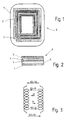
- Fig. 1 shows an embodiment of the invention
- Resonant circuit 6 in plan view. 2 is the in Fig. 1 shown resonant circuit 6 in cross section see.
- Deactivation of the resonant circuit 6 done by shorting between the two spiral Conductor tracks 2, 3, which are preferably made of aluminum are manufactured, through the dielectric layer 4 is produced.
- An applied alternating magnetic field, like it e.g. is emitted by the monitoring system AC voltages in the two spiral conductor tracks 2, 3 of the resonant circuit 6.
- the spiral Conductor tracks 2, 3 at least partially overlap and are in opposite directions wrapped.
- the exterior End of the lower coil 2 has a positive potential relative to inner end of the lower coil 2 when the inner end the upper coil 3 has a positive potential with respect to the has the outer end of the upper coil 3. So it stays to note that the points / areas in which the induced alternating voltages between the two coils 2, 3 are maximum, located in the end regions of the coils 2, 3.
- the upper coil 3 Since in the example shown in FIG. 1 the upper coil 3 has fewer turns than the lower coil 2, the highest voltages between the ends of the upper coil 3 and the positions directly below the lower coil 2 generated.
- Fig. 3 illustrates the voltage relationships in different areas of the two themselves at least partially overlapping coils 2, 3 of a resonant circuit 6, according to an advantageous development of the resonant circuit 6 according to the invention used can be.
- the dielectric layer 4 breaks open these local vulnerabilities together, although the potential for tension here is lower than at the ends of the top Coil 2 and lower coil 3. Since the voltage potential at the local vulnerabilities is less than at the ends of the Conductor tracks 2, 3 are those for generating the deactivation short circuit available electrical energy less than the electrical energy needed to generate one Deactivation short circuit at the ends of the upper coil 3 would be necessary.
- Fig. 5 shows a cross section through a dielectric Layer with manufacturing defects, here air bubbles 7 and Irregularities in the surface.
- the dielectric layer is to avoid manufacturing defects 4 trained according to a further training that they in essentially has a uniform thickness and large Part is free from local vulnerabilities 7.
- Such uniform dielectric layer 4 provides a Deactivation in the end areas of the spiral Conductor tracks 2, 3 safe, since here the induced voltage and Energy are maximum. A short circuit caused by a such deactivation arises, is very robust and little susceptible to inadvertent reactivation.
- the resonant circuit 6 consists of the dielectric layer 4 from at least two components 4a, 4b, an upper one Component 4a and a lower component 4b.
- the lower one Component 4b is stamped onto the lower coil 3 applied.
- the upper component 4a is on the upper coil 2 applied.
- the upper component has 4a a relatively low melting point, which allows her to serve as a hot melt adhesive and the two coils 2, 3 during the hot stamping of the upper coil 2 onto the lower one Glue coil 3.
- the upper component 4a of the dielectric Layer 4 melts during hot stamping of the top coil 2.
- the lower component 4b of the dielectric layer 4 has a higher melting point and does not melt during the Hot stamping on the top spool 2.
- the uniformity of the lower component 4b of the dielectric layer 4 which is not melts, improves the uniformity in the thickness of the dielectric layer 4 overall.
- Fig. 6 shows a cross section through a resonant circuit 6 with a dielectric layer 4 consisting of two Components 4a, 4b.
- the lower component 4b can either by coating the lower coil 3 or by Laminating the lower component 4b of the dielectric Layer 4 are produced on the coil 3.
- the coil material (A1) in the form of wide Roll material before, so that the uniformity of the surface the dielectric layer 4 can be maintained and other defects, for example, by Air pockets 7 are caused to be minimized.
- the resonant circuit 6 is local in the Area of the ends of the upper coil 2 or in the area of prepared area reinforced.
- the reinforced zone 10 is less prone to shear and glide or a Delaminate.
- everyone can Strain on the resonant circuit 6 by buckling or Bends are reduced because the two are spiral Conductor tracks 2, 3 only nearby, but not within the locally reinforced zone 10 shear, slide, kink or delaminate.
- Resonant circuit 6 are the areas around the ends one of the two conductor tracks 2, 3, here the upper one Conductor 2, reinforced by the fact that a local zone 10 with an additional pressure is applied, the metal, preferably aluminum, is shaped so that it is a non-plane Takes shape.
- the local pressurization causes better adhesion between the two conductor tracks 2, 3 and between the lower conductor track 3 and the dielectric layer 4. Is this pressure by means of a shaping tool 11 with a survey with a preset profile (stamp 12), the Traces 2,3 are shaped so that the resistance of the Resonant circuit 6 significantly against reactivation is improved.
- the tool 11 can also be flat be formed and have predetermined dimensions.
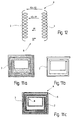
- Fig. 7 shows a plan view of an embodiment of a reinforced zone 10 at one end of the upper conductor track 2.
- Fig. 8a is a cross section and in Fig. 8b is a plan view a tool 11 shown for the manufacture of the reinforced zone 10 can be used.
- Training the weakened zone 13 can be done either by the Width of the conductor track 2, 3 is narrowed, as in FIG. 9 and Fig. 10, or by corresponding Treatment of the adhesive layer in this weakened zone 13, in such a way that the bond between the Conductor tracks 2, 3 is considerably weaker here.
- Another One way to get weakened zones 13 is to to perforate the conductor tracks 2, 3.
- FIG. 12 The equivalent circuit diagram of this arrangement is shown in FIG. 12 shown.
- the generated between the two coils 2, 3 Voltage difference is at the outer coil ends is much larger than anywhere else between the coils 2, 3.
- Figures 11c and 12 also show that the outer turn of the lower conductor track 3 from the upper To a large extent, conductor track 2 is not covered at all becomes.
- this overlap-free section 9 there is also no deactivation. If you follow them outer turn of the lower conductor track 3 from the end point back where there is a small overlap area with the upper trace 2 there, it is found that the next Point at which there is an overlap of the conductor tracks 2, 3 and thus there is a possibility of deactivation, one piece back on the outer turn of the lower conductor track 3 lies. This point has a much lower one Voltage potential between upper and lower conductor track 2, 3rd
- Another advantage is that due to the uneven distribution of the potential difference along the Conductor tracks 2, 3 for a deactivation short circuit available energy between the conductor tracks 2, 3 is higher must as with an even distribution of tension and Capacity. However, higher energy means one more reliable short circuit and thus also automatically less risk of unwanted reactivation.
Abstract
Description
Die Erfindung betrifft ein Sicherungselement für die elektronische Artikelsicherung, bestehend aus zumindest einer spiralförmigen Leiterbahn und einem Kondensator mit einer dazwischen befindlichen dielektrischen Schicht oder bestehend aus zwei spiralförmigen Leiterbahnen, die zumindest teilweise überlappend zu beiden Seiten einer dielektrischen Schicht angeordnet sind (→ Resonanzschwingkreis).The invention relates to a fuse element for the electronic Article security, consisting of at least one spiral conductor track and a capacitor with a intermediate dielectric layer or existing from two spiral conductor tracks, which are at least partially overlapping on both sides of a dielectric layer are arranged (→ resonant circuit).
Resonanzschwingkreise, die bei einer vorgegebenen Resonanzfrequenz, die üblicherweise bei 8.2 MHz liegt, zu Resonanzschwingungen angeregt werden, sind zur Sicherung von Waren gegen Diebstahl in Warenhäuser allgemein gebräuchlich. Oftmals sind Sie integraler Teil von Klebeetiketten oder Hängeetiketten aus Karton, die an den zu sichernden Artikeln befestigt sind. Typischerweise ist das Warenhaus mit einem elektronischen Überwachungssystem im Ausgangsbereich ausgestattet, das die Resonanzschwingkreise erkennt und einen Alarm auslöst, wenn ein gesicherter Artikel in unerlaubter Weise eine gesicherte Überwachungszone passiert. Sobald ein Kunde die Ware bezahlt hat, wird der Resonanzschwingkreis deaktiviert. Durch die Maßnahme wird verhindert, daß ein Alarm ausgelöst wird, sobald ein Artikel rechtmäßig erworben worden ist und nachfolgend die Überwachungszone passiert.Resonance resonant circuits, which at a predetermined resonance frequency, which is usually 8.2 MHz, to resonance vibrations are encouraged to secure goods common against theft in department stores. They are often an integral part of adhesive labels or Cardboard hang tags attached to the items to be secured are attached. Typically, the department store is with one electronic surveillance system in the exit area equipped that recognizes the resonant circuits and one Alarm triggers when a secured item is in an unauthorized manner Way a secured surveillance zone happens. Once a Customer has paid for the goods, the resonant circuit deactivated. The measure prevents a Alarm is triggered as soon as an item is lawfully purchased has been passed and subsequently the surveillance zone.
Die Deaktivierungssysteme, die oft in den Kassenbereichen plaziert sind, erzeugen ein Resonanzsignal mit einer größeren Amplitude als sie in den Überwachungssystemen erzeugt wird. Ein Resonanzetikett wird normalerweise in einer Feldstärke, die größer ist als 1,5 A/m, deaktiviert. Bekannt geworden sind unterschiedliche Deaktivierungsmechanismen für Resonanzschwingkreise. Entweder wird die Isolation zwischen einander gegenüberliegenden Leiterbahnen zerstört, wodurch ein Kurzschluß entsteht, oder ein Stück einer Leiterbahn wird überlastet und schmilzt, wodurch eine Unterbrechung entsteht. Als Folge der Deaktivierung werden die resonanten Eigenschaften des Resonanzschwingkreises, d.h. die Resonanzfrequenz und/oder der "Q"-Faktor derart stark modifiziert, daß das Resonanzetikett nicht mehr durch das Überwachungssystem detektiert wird.The deactivation systems, often in the checkout areas placed produce a resonance signal with a larger one Amplitude as it is generated in the surveillance systems. A resonance label is usually in a field strength, which is greater than 1.5 A / m, deactivated. Known are different deactivation mechanisms for Resonant circuits. Either the isolation between opposing interconnects destroyed, whereby a short circuit occurs or a piece of a conductor track becomes overloads and melts, causing an interruption. As a result of the deactivation, the resonant properties of the resonant circuit, i.e. the resonance frequency and / or the "Q" factor is modified so much, that the resonance label is no longer through the surveillance system is detected.
Der deaktivierte Resonanzschwingkreis kann durch mechanische Manipulation, beispielsweise durch Knicken, Einpacken und Transportieren der Ware oder durch eine Biegung des Etiketts und damit des Resonanzschwingkreises, unbeabsichtigt wieder reaktiviert werden. Eine unbeabsichtigte Reaktivierung eines Resonanzschwingkreises, der an einem rechtmäßig erworbenen Artikel befestigt ist, kann dann zur Auslösung eines Alarms führen, was ein ziemliches Ärgernis sowohl für den Käufer als auch für das Warenhaus darstellt.The deactivated resonant circuit can be mechanically Manipulation, for example by kinking, packing and Transporting the goods or by bending the label and thus the resonant circuit, unintentionally again be reactivated. An unintentional reactivation of one Resonant circuit which is based on a lawfully acquired Item attached, can then trigger an alarm perform what is quite a nuisance to both the buyer and also represents for the department store.
Bislang ist kein Stand der Technik bekannt geworden, der sich mit dem Problem der Verringerung des Risikos einer unbeabsichtigten Reaktivierung von bereits deaktivierten Resonanzetiketten befaßt. Bezüglich der Deaktivierung von Resonanzetiketten sind unterschiedliche Verfahren beschrieben worden. To date, no state of the art has become known with the problem of reducing the risk of accidental Reactivation of already deactivated resonance labels deals. Regarding the deactivation of resonance labels different methods have been described.
In der US-PS 4,876,555 bzw. in der entsprechenden EP 0285 559 B1 wird vorgeschlagen, mittels einer Nadel ein Loch in der Isolationsschicht zwischen zwei gegenüberliegenden Kondensatorflächen zu erzeugen. Hierdurch wird ein Deaktivierungsmechanismus hergestellt, der fehlerfrei und dauerhaft ist.In US Pat. No. 4,876,555 or in the corresponding EP 0285 559 B1 proposes a hole in the by means of a needle Insulation layer between two opposite To generate capacitor areas. This will be a Deactivation mechanism made that is error free and is permanent.
Auch die US-PS 5,187,466 beschreibt ein Verfahren zur Erzeugung eines deaktivierbaren Resonanzschwingkreises mittels eines Kurzschlusses, der unter normalen Umständen nicht zerstört werden kann.US Pat. No. 5,187,466 also describes a method for Generation of a deactivatable resonant circuit by means of a short circuit which, under normal circumstances cannot be destroyed.
Bezüglich der zuerst genannten US-PS 4,876,555 bzw. der EP 0
285 559 B1 sollte angemerkt werden, daß der dort offenbarte
Resonanzschwingkreis Kondensatorplatten aufweist, die auf
beiden Seiten des Dielektrikums angeordnet sind. Die zwischen
den beiden Kondensatorplatten liegende dielektrische Schicht
weist ein durchgehendes Loch auf.With regard to the first-mentioned US Pat. No. 4,876,555 and
In der bereits erwähnten US-PS 5,187,466 wird ein Verfahren beschrieben, das auf einen Resonanzschwingkreis mit Kondensatorplatten auf beiden Seiten des Dielektrikums angewendet wird, wobei die Kondensatorplatten erst kurzgeschlossen werden und der Kurzschluß später durch Beaufschlagung mit elektrischer Energie geschmolzen wird.A process is described in the previously mentioned US Pat. No. 5,187,466 described that with a resonant circuit Capacitor plates on both sides of the dielectric is applied, the capacitor plates first be short-circuited and the short-circuit later Electric power is melted.
Es sind noch andere wichtige Techniken auf dem Gebiet der
Deaktivierung von Resonanzetiketten bekannt geworden, die
sich jedoch ebenfalls nicht mit der Verringerung des Risikos
einer unbeabsichtigten Reaktivierung befassen. Eine
Patentfamilie, die in diese Richtung geht, umfaßt u.a. die EP
0 181 327 Bl, die US-PS 4,567,473 und die US-PS 4,498,076.
Das in diesen Patenten beschriebene erfindungsgemäße
Resonanzetikett setzt sich wie folgt zusammen: ein
Trägermaterial, das als Dielektrikum dient, Kondensatorplatten
auf beiden Seiten des planaren, dielektrischen
Trägermaterials, eine Deaktivierungszone und ein Schwingkreis,
der auf dem Dielektrikum angeordnet ist. Der Stand der
Technik nennt bislang keinerlei Maßnahmen, die eine
ungewollte Reaktivierung nach erfolgreicher Deaktivierung
verhindern.There are other important techniques in the field of
Deactivation of resonance labels has become known
however, also does not deal with reducing the risk
deal with unintended reactivation. A
Patent family that goes in this direction includes the
Der Erfindung liegt die Aufgabe zugrunde, einen Resonanzschwingkreis mit einer reduzierten Reaktivierungswahrscheinlichkeit vorzuschlagen.The invention has for its object a resonant circuit with a reduced probability of reactivation to propose.
Die Aufgabe wird dadurch gelöst, daß in der dielektrischen Schicht zumindest ein ausgewählter Bereich (eine Soll-Durchbruchstelle) vorgesehen ist, in dem bei einer entsprechend hohen Energiezufuhr durch ein magnetisches Wechselfeld ein Kurzschluß zwischen den gegenüberliegenden Kondensatorplatten oder den spiralförmigen Leiterbahnen geschaffen wird, und wobei der ausgewählte Bereich lokal derart verstärkt ist, daß eine Zerstörung des Kurzschlusses (=leitfähiger Pfad) durch mechanische Beanspruchung und somit eine Reaktivierung des Sicherungselementes verhindert wird.The object is achieved in that in the dielectric Layer at least one selected area (a target breakthrough point) is provided in which at a correspondingly high energy supply through a magnetic Alternating field a short circuit between the opposite Capacitor plates or the spiral conductor tracks is created, and where the selected area is local is so amplified that destruction of the short circuit (= conductive path) due to mechanical stress and thus reactivation of the securing element is prevented.
Gemäß einer vorteilhaften Weiterbildung des erfindungsgemäßen Sicherungselementes ist vorgesehen, daß die dielektrische Schicht im wesentlichen eine gleichmäßige Dicke und keine zusätzlichen Fertigungsfehler (z.B. Lufteinschlüsse) aufweist.According to an advantageous development of the invention Fuse element is provided that the dielectric layer essentially a uniform thickness and no additional manufacturing defects (e.g. air pockets) having.
Weiterhin wird vorgeschlagen, daß im Falle von zwei zumindest teilweise überlappenden Leiterbahnen diese in entgegengesetzten Richtungen gewickelt sind, wobei der ausgewählte Bereich an den äußeren Enden der Leiterbahnen liegt. Hier tritt nämlich die höchste Induktionsspannung auf.It is further proposed that in the case of two at least partially overlapping traces these in opposite Directions are wound, the selected one Area lies at the outer ends of the conductor tracks. Here namely the highest induction voltage occurs.
Eine vorteilhafte Ausbildung des erfindungsgemäßen Sicherungselementes schlägt vor, die dielektrische Schicht in dem ausgewählten Bereich dünner auszubilden als in den verbleibenden Bereichen.An advantageous embodiment of the invention Fuse element suggests the dielectric layer in to make the selected area thinner than in the remaining areas.
Gemäß einer Alternative ist der ausgewählte Bereich dadurch ausgezeichnet, daß die dielektrische Schicht hier eine andere chemische oder physikalische Beschaffenheit aufweist als in den verbleibenden Bereichen.According to an alternative, the selected area is thereby excellent that the dielectric layer here is another has chemical or physical properties as in the remaining areas.
Gemäß einer vorteilhaften Weiterbildung des erfindungsgemäßen Sicherungselementes besteht die dielektrische Schicht aus zumindest zwei Komponenten. In diesem Zusammenhang ist es besonders günstig, wenn der Schmelzpunkt der einen Komponente der dielektrischen Schicht oberhalb der Fertigungstemperatur für Sicherungselemente liegt. Weiterhin sieht eine Ausgestaltung vor, daß die Komponenten der dielektrischen Schicht derart beschaffen sind, daß sie entweder durch Beschichtung oder durch Laminierung hergestellt werden.According to an advantageous development of the invention Fuse element consists of the dielectric layer from at least two components. In this context it is particularly favorable if the melting point of one component the dielectric layer above the manufacturing temperature for securing elements. Furthermore one sees Design before that the components of the dielectric Layer are such that they can either by Coating or by lamination.
Gemäß einer vorteilhaften Ausgestaltung des erfindungsgemäßen Sicherungselementes wird der ausgewählte Bereich, in dem die Deaktivierung stattfindet, durch die Beaufschlagung mit zusätzlichem Druck verstärkt. Durch das Zusammendrücken wird die Haftung zwischen den Kondensatorplatten bzw. den sich zumindest teilweise überlappenden Leiterbahnen verbessert. Als günstig hat es sich erwiesen, wenn die Verstärkung durch Druckformen der Kondensatorplatten bzw. der sich zumindest teilweise überlappenden Leiterbahnen in eine dreidimensionale Form erzielt wird. Hierbei ist es besonders vorteilhaft, wenn die verbesserte Haftung und das Formen der Kondensatorplatten bzw. der Leiterbahnen in einem Vorgang erreicht werden.According to an advantageous embodiment of the invention Security element is the selected area, in the deactivation takes place through the application reinforced with additional pressure. By squeezing the liability between the capacitor plates or at least partially overlapping conductor tracks improved. It has proven to be favorable if the Reinforcement by printing the capacitor plates or at least partially overlapping conductor tracks into one three-dimensional shape is achieved. It is special here advantageous if the improved adhesion and the shaping of the Capacitor plates or the conductor tracks in one process can be achieved.
Kommt es zu einem Verbiegen oder Umknicken des Resonanzschwingkreises im Bereich der verstärkten Zone, in der ja auch die Deaktivierung stattfindet, besteht immer noch die Gefahr des Verziehens, der Abscherung, Verschiebung oder Ablösung des Resonanzschwingkreises an der Deaktivierungsstelle. Dadurch würde der Resonanzschwingkreis in unerwünschter Weise wieder aktiviert werden. Um dieser Gefahr vorzubeugen, ist gemäß einer Weiterbildung der Erfindung vorgesehen, beiderseits der verstärkten Zone geschwächte Zonen auszubilden. Greift ein Biegemoment von außen an, so ist die Wahrscheinlichkeit, daß der Resonanzschwingkreis im Bereich der geschwächten Zonen umknickt oder sogar bricht, viel größer als ein Umbiegen oder Brechen innerhalb der verstärkten Zone. Die geschwächte Zone kann daher auch als die bevorzugte Biege- oder Bruchzone bezeichnet werden.If the resonant circuit is bent or bent in the area of the reinforced zone, in the yes the deactivation takes place, there is still the Risk of warping, shearing, shifting or Replacement of the resonant circuit at the deactivation point. This would cause the resonant circuit in undesirably reactivated. To this danger to prevent, is according to a development of the invention provided weakened on both sides of the reinforced zone Train zones. Attacks a bending moment from the outside, so is the probability that the resonant circuit in the Area of the weakened zones is bent or even breaks, much larger than bending or breaking within the reinforced zone. The weakened zone can therefore also be used as the preferred bending or breaking zone.
Die Ausbildung der geschwächten Zonen kann einmal dadurch erfolgen, daß die Breite der Leiterbahn verengt wird. Eine weitere Möglichkeit besteht darin, daß die Klebstoffschicht in diesen geschwächten Zonen so behandelt ist, daß die Bindung zwischen den spiralförmigen Leiterbahnen erheblich reduziert ist. Weiterhin ist es möglich, die Leiterbahnen in den geschwächten Zonen zu perforieren.The formation of the weakened zones can do this take place that the width of the conductor track is narrowed. A another possibility is that the adhesive layer in these weakened zones is treated in such a way that the Binding between the spiral conductor tracks considerably is reduced. It is also possible to trace the tracks in to perforate the weakened zones.
Gemäß einer vorteilhaften Weiterbildung der Erfindung ist der Resonanzschwingkreis so ausgebildet, daß die Kapazität zwischen oberer und unterer Leiterbahn an den inneren Enden der Spulen konzentriert wird. Insbesondere ist an den inneren Enden der Spulen ein großer Überlappungsbereich der Leiterbahnen vorgesehen, woraus sich eine entsprechend große Kapazität ergibt, während die Überlappung an den äußeren Spulenenden sehr gering ist.According to an advantageous development of the invention Resonant circuit designed so that the capacity between the upper and lower conductor tracks at the inner ends the coils are concentrated. In particular is on the inner Ends of the coils a large area of overlap Conductor tracks provided, resulting in a correspondingly large Capacity results while the overlap on the outer Coil ends is very low.
Eine vorteilhafte Weiterbildung der erfindungsgemäßen Vorrichtung schlägt vor, daß sich die Überlappungsbereiche zwischen den beiden Leiterbahnen und somit die Kapazität zwischen den Leiterbahnen an den inneren Enden der Leiterbahnen konzentrieren. Insbesondere ist vorgesehen, daß die äußeren Enden der beiden Leiterbahnen in einem kleinen Bereich überlappen und daß sich an die äußeren Enden der Leiterbahnen ein relativ langer überlappungsfreier Bereich anschließt. Ein Vorteil dieser Topologie besteht darin, daß die Deaktivierung im Überlappungsbereich zwischen den äußeren Enden von oberer und unterer Leiterbahn stattfindet, da dies die Stelle mit dem höchsten Spannungspotential zwischen den Leiterbahnen ist.An advantageous development of the invention Device suggests that the overlap areas between the two conductor tracks and thus the capacity between the traces at the inner ends of the Concentrate conductor tracks. In particular, it is provided that the outer ends of the two traces in a small one Area overlap and that is at the outer ends of the Conductors a relatively long area without overlap connects. An advantage of this topology is that deactivation in the overlap area between the outer ones Ends of the upper and lower trace takes place as this the point with the highest voltage potential between the Conductor tracks is.
Die Deaktivierungsstelle ist daher mit hoher Sicherheit im ausgewählten Bereich angesiedelt.The deactivation point is therefore very safe in the selected area.
Die Erfindung wird anhand der nachfolgenden Figuren näher
erläutert. Es zeigt:
Fig. 1 zeigt eine Ausführungsform des erfindungsgemäßen
Resonanzschwingkreises 6 in Draufsicht. In Fig. 2 ist der in
Fig. 1 gezeigte Resonanzschwingkreis 6 im Querschnitt zu
sehen. Die Deaktivierung des Resonanzschwingkreises 6
erfolgt, indem ein Kurzschluß zwischen den beiden spiralförmigen
Leiterbahnen 2, 3, die vorzugsweise aus Aluminium
gefertigt sind, durch die dielektrische Schicht 4 hindurch
erzeugt wird. Ein angelegtes magnetisches Wechselfeld, wie es
z.B. von dem Überwachungssystem ausgesendet wird, induziert
Wechselspannungen in die beiden spiralförmigen Leiterbahnen
2, 3 des Resonanzschwingkreises 6. Die spiralförmigen
Leiterbahnen 2, 3, überlappen zumindest teilweise und sind in
entgegengesetzte Richtungen gewickelt. Daher weist das äußere
Ende der unteren Spule 2 ein positives Potential relativ zum
inneren Ende der unteren Spule 2 auf, wenn das innere Ende
der oberen Spule 3 ein positives Potential bezüglich des
äußeren Endes der oberen Spule 3 hat. Es bleibt also
festzuhalten, daß sich die Punkte/Bereiche, in denen die
induzierten Wechselspannungen zwischen den beiden Spulen 2, 3
maximal sind, in den Endbereichen der Spulen 2, 3 befinden.Fig. 1 shows an embodiment of the invention
Da in dem in Fig. 1 gezeigten Beispiel die obere Spule 3
weniger Windungen besitzt als die untere Spule 2, werden die
höchsten Spannungen zwischen den Enden der oberen Spule 3 und
den direkt darunterliegenden Stellen der unteren Spule 2
erzeugt.Since in the example shown in FIG. 1 the
Fig. 3 verdeutlicht die Spannungsverhältnisse in
unterschiedlichen Bereichen der beiden sich zumindest
teilweise überlappenden Spulen 2, 3 eines Resonanzschwingkreises
6, der gemäß einer vorteilhaften Weiterbildung
des erfindungsgemäßen Resonanzschwingkreises 6 verwendet
werden kann.Fig. 3 illustrates the voltage relationships in
different areas of the two themselves at least
partially overlapping
Bei dem zuvor beschriebenen Resonanzschwingkreis 6 mit
gleichmäßiger Dicke der dielektrischen Schicht 4 zwischen den
Spulen 2, 3 erfolgt die Deaktivierung in den Endbereichen von
oberer Spule 3 und unterer Spule 2, da hier das induzierte
Potential maximal ist. Da die elektrische Feldstärke
konzentriert an einer Oberfläche mit kleinem Radius auftritt,
kommt es zu einer Deaktivierung genau an den Enden der
Leiterbahnen 2, 3 - wie in Fig. 4 gezeigt.With the
Wenn jedoch die dielektrische Schicht 4 nicht gleichmäßig
dick ist oder Luftblasen 7 enthält, was aufgrund von
Fertigungsfehlern durchaus möglich ist, kann eine
Deaktivierung in verschiedenen Bereichen der Spulen 2, 3
auftreten. Solche Fertigungsfehler können örtliche
Schwachstellen verursachen und sogar Löcher durch
Lufteinschlüsse 7 in der dielektrischen Schicht 4
hervorrufen. Hierdurch bricht die dielektrische Schicht 4 an
diesen lokalen Schwachstellen zusammen, obwohl das Spannungspotential
hier niedriger ist als an den Enden von oberer
Spule 2 und unterer Spule 3. Da das Spannungspotential an den
lokalen Schwachstellen geringer ist als an den Enden der
Leiterbahnen 2, 3, ist die zur Erzeugung des Deaktivierungskurzschlusses
zur Verfügung stehende elektrische Energie
kleiner als die elektrische Energie, die zur Erzeugung eines
Deaktivierungskurzschlusses an den Enden der oberen Spule 3
notwendig wäre.However, if the
Fig. 5 zeigt einen Querschnitt durch eine dielektrische
Schicht mit Fertigungsfehlern, hier Luftblasen 7 und
Unregelmäßigkeiten im Bereich der Oberfläche. Um derartige
Fertigungsfehler zu vermeiden, ist die dielektrische Schicht
4 gemäß einer Weiterbildung so ausgebildet, daß sie im
wesentlichen eine gleichmäßige Dicke aufweist und zum großen
Teil frei ist von lokalen Schwachstellen 7. Eine solch
gleichmäßige dielektrische Schicht 4 stellt eine
Deaktivierung in den Endbereichen der spiralförmigen
Leiterbahnen 2, 3 sicher, da hier die induzierte Spannung und
Energie maximal sind. Ein Kurzschluß, der durch eine
derartige Deaktivierung entsteht, ist sehr robust und wenig
anfällig für unbeabsichtigtes Reaktivieren.Fig. 5 shows a cross section through a dielectric
Layer with manufacturing defects, here air bubbles 7 and
Irregularities in the surface. To such
The dielectric layer is to avoid
Gemäß einer vorteilhaften Weiterbildung des erfindungsgemäßen
Resonanzschwingkreises 6 besteht die dielektrische Schicht 4
aus zumindest zwei Komponenten 4a, 4b, einer oberen
Komponente 4a und einer unteren Komponente 4b. Die untere
Komponente 4b wird vor dem Abstanzen und Heißprägen auf die
untere Spule 3 aufgebracht. Die obere Komponente 4a wird auf
die obere Spule 2 aufgebracht. Die obere Komponente 4a hat
einen relativ niedrigen Schmelzpunkt, der es ihr ermöglicht,
als Schmelzklebstoff zu dienen und die beiden Spulen 2, 3
während des Heißprägens der oberen Spule 2 auf die untere
Spule 3 zu kleben. Die obere Komponente 4a der dielektrischen
Schicht 4 schmilzt während des Heißprägens der oberen Spule
2. Die untere Komponente 4b der dielektrischen Schicht 4 hat
einen höheren Schmelzpunkt und schmilzt nicht während des
Heißprägens auf die obere Spule 2. Die Gleichmäßigkeit der
unteren Komponente 4b der dielektrischen Schicht 4, die nicht
schmilzt, verbessert die Gleichmäßigkeit in der Dicke der
dielektrischen Schicht 4 insgesamt.According to an advantageous development of the invention
The
Fig. 6 zeigt einen Querschnitt durch einen Resonanzschwingkreis
6 mit einer dielektrischen Schicht 4, die aus zwei
Komponenten 4a, 4b besteht. Die untere Komponente 4b kann
entweder durch Beschichtung der unteren Spule 3 oder durch
Laminierung der unteren Komponente 4b der dielektrischen
Schicht 4 auf die Spule 3 hergestellt werden. Üblicherweise
liegt das Spulenmaterial (A1) in Form von breitem
Rollenmaterial vor, so daß die Gleichmäßigkeit der Oberfläche
der dielektrischen Schicht 4 aufrechterhalten werden kann und
andere Fehlerstellen, die beispielsweise durch
Lufteinschlüsse 7 hervorgerufen werden, minimiert werden.Fig. 6 shows a cross section through a
Es kann vorkommen, daß der Kurzschluß durch Knicken oder
andere mechanische Manipulationen aufgebrochen wird, selbst
wenn die dielektrische Schicht 4 so gleichmäßig ist, daß
Defekte 7 weitgehend reduziert sind und der Deaktivierungskurzschluß
ausschließlich am Ende der oberen Leiterbahn
auftritt, wo die induzierte Energie maximal ist. (Dies ist
natürlich nur der Fall, wenn keine anderweitig präparierte
Druchbruchstelle vorgesehen.) Scher- oder Gleitbewegungen der
zwei Metallschichten relativ zu einander oder Delaminierung
der beiden Schichten können zu einer unbeabsichtigten
Reaktivierung führen.It can happen that the short circuit by kinking or
other mechanical tampering is broken up, even
if the
Erfindungsgemäß ist der Resonanzschwingkreis 6 lokal im
Bereich der Enden der oberen Spule 2 bzw. im Bereich des
präparierten Bereichs verstärkt. Die verstärkte Zone 10 ist
weniger anfällig für Scher- und Gleitbewegungen oder ein
Delaminieren. Durch lokale Verstärkung kann jede
Beanspruchung des Resonanzschwingkreises 6 durch Knicken oder
Biegen verringert werden, da die beiden spiralförmigen
Leiterbahnen 2, 3 nur in der Nähe, aber nicht innerhalb der
lokal verstärkten Zone 10 scheren, gleiten, knicken oder
delaminieren.According to the
Gemäß einer vorteilhaften Weiterbildung des erfindungsgemäßen
Resonanzschwingkreises 6 werden die Bereiche um die Enden
einer der beiden Leiterbahnen 2, 3, hier der oberen
Leiterbahn 2, dadurch verstärkt, daß eine lokale Zone 10 mit
einem zusätzlichen Druck beaufschlagt wird, wobei das Metall,
vorzugsweise Aluminium, so geformt wird, daß es eine nichtebene
Form annimmt. Die örtliche Beaufschlagung mit Druck
bewirkt eine bessere Haftung zwischen den beiden Leiterbahnen
2, 3 und zwischen der unteren Leiterbahn 3 und der
dielektrischen Schicht 4. Wird dieser Druck mittels eines
formgebenden Werkzeugs 11 mit einer Erhebung mit einem
vorgegebenen Profil (Stempel 12) beaufschlagt, können die
Leiterbahnen 2,3 so geformt werden, daß die Resistenz des
Resonanzschwingkreises 6 gegen Reaktivierung erheblich
verbessert wird. Das Werkzeug 11 kann übrigens auch flach
ausgebildet sein und vorgegebene Abmessungen aufweisen.According to an advantageous development of the invention
Hinsichtlich der strukturellen Eigenschaften von Metallen ist
es wohlbekannt, daß ein Metallblech mit Rillen, Wölbungen
oder anderen eingearbeiteten Strukturen sich nicht so leicht
biegen läßt wie ein flaches Blech. Das gleiche Prinzip wird
hier angewendet, um eine lokal verstärkte Zone 10 zu
erzeugen. Jedes großflächige Falten oder Biegen des
Resonanzschwingkreises 6 führt dazu, den Resonanzschwingkreis
6 in der Nähe aber nicht innerhalb der verstärkten Zone 10 zu
biegen, zu falten, zu scheren oder zu delaminieren. So wird
das Risiko einer unbeabsichtigten Reaktivierung verringert.
Die tatsächliche Form der verstärkten Zone 10 ist nicht
ausschlaggebend, das tatsächliche Profil der geformten
Leiterbahn 2, 3 in der verstärkten Zone 10 ist auch nicht
kritisch.Regarding the structural properties of metals
it is well known that a metal sheet with grooves, bulges
or other incorporated structures are not so easy
bends like a flat sheet. The same principle will
applied here to a locally reinforced
Fig. 7 zeigt eine Draufsicht auf eine Ausführungsform einer
verstärkten Zone 10 am einen Ende der oberen Leiterbahn 2.Fig. 7 shows a plan view of an embodiment of a
reinforced
In Fig. 8a ist ein Querschnitt und in Fig. 8b eine Draufsicht
eines Werkzeug 11 gezeigt, das zur Herstellung der
verstärkten Zone 10 verwendet werden kann.In Fig. 8a is a cross section and in Fig. 8b is a plan view
a
Kommt es zu einem Verbiegen oder Umknicken des Resonanzschwingkreises
6 im Bereich der verstärkten Zone 10, also der
Zone, in der bekanntermaßen die Deaktivierung stattfindet und
die. absichtlich verstärkt worden ist, besteht hier immer noch
die Gefahr einer Verziehung, Abscherung, Verschiebung oder
Ablösung des Resonanzschwingkreises 6. Dies würde zu einer
unerwünschten Reaktivierung des Resonanzschwingkreises 6
führen. Um dieser Gefahr vorzubeugen, ist in einer
zusätzlichen Weiterbildung der Erfindung vorgesehen,
beiderseits der verstärkten Zone 10 geschwächte Zonen 13
auszubilden. Greift ein Biegemoment von außen her an, so ist
es wahrscheinlich, daß der Resonanzschwingkreis 6 im Bereich
der geschwächten Zonen 13 umknickt oder sogar bricht. Die
geschwächte Zone 13 kann daher auch als die bevorzugte Biege-
oder Bruchzone bezeichnet werden. Die Ausbildung der
geschwächten Zone 13 kann entweder dadurch erfolgen, daß die
Breite der Leiterbahn 2, 3 verengt wird, wie in den Fig. 9
und Fig. 10 dargestellt, oder auch durch entsprechende
Behandlung der Klebstoffschicht in dieser geschwächten Zone
13, und zwar in der Weise, daß die Bindung zwischen den
Leiterbahnen 2, 3 hier erheblich schwächer ist. Eine weitere
Möglichkeit, geschwächte Zonen 13 zu erhalten, besteht darin,
die Leiterbahnen 2, 3 zu perforieren.If the resonant circuit is bent or bent
6 in the area of the reinforced
Gemäß einer zusätzlichen Weiterbildung der Erfindung sind die
Leiterbahnen 2, 3 und der Resonanzschwingkreis 6 so
ausgebildet, daß die Kapazität zwischen oberer und unterer
Leiterbahn 2, 3 an den inneren Enden der spiralförmigen
Leiterbahnen 2, 3 konzentriert wird. Die Figuren Fig. 11a,
Fig. 11b und Fig. 11c zeigen einen entsprechenden Resonanzschwingkreis
6. Aus den Figuren ist zu ersehen, daß an den
inneren Enden der Spulen 2, 3 ein großer Überlappungsbereich
der Leiterbahnen 2, 3 vorhanden ist, woraus sich eine
proportional große Kapazität ergibt, während die Überlappung
an den äußeren Enden der Spulen 2, 3 sehr gering ist.According to an additional development of the invention
Conductor tracks 2, 3 and the
Das Ersatzschaltbild dieser Anordnung ist in Figur 12
dargestellt. Der zwischen den beiden Spulen 2, 3 erzeugte
Spannungsunterschied ist an den äußeren Spulenenden
wesentlich größer ist als an jeder anderen Stelle zwischen
den Spulen 2, 3. Bei einer gemeinsamen Betrachtung der
Figuren Fig. 11c und Fig. 12 ist auch festzustellen, daß die
äußere Windung der unteren Leiterbahn 3 von der oberen
Leiterbahn 2 zu einem großen Teil überhaupt nicht überdeckt
wird. Somit kann entlang dieses überlappungsfreien Abschnitts
9 auch keine Deaktivierung stattfinden. Verfolgt man die
äußere Windung der unteren Leiterbahn 3 vom Endpunkt an
zurück, wo es einen kleinen Überlappungsbereich mit der
oberen Leiterbahn 2 gibt, so stellt man fest, daß der nächste
Punkt, an dem eine Überlappung der Leiterbahnen 2, 3 und
somit die Möglichkeit der Deaktivierung besteht, ein Stück
zurück auf der äußeren Windung der unteren Leiterbahn 3
liegt. Dieser Punkt hat ein erheblich geringeres
Spannungspotential zwischen oberer und unterer Leiterbahn 2,
3.The equivalent circuit diagram of this arrangement is shown in FIG. 12
shown. The generated between the two
Selbst wenn die dielektrische Schicht 4 zwischen den beiden
Leiterbahnen nicht von absolut gleichmäßiger Dicke oder nicht
absolut frei von sonstigen Schwachstellen 7 ist, findet die
Deaktivierung an dieser äußeren Überlappungsstelle statt, da
an dieser Stelle eine erheblich höhere Potentialdifferenz
zwischen den Leiterbahnen 2, 3 vorhanden ist. Even if the
Ein weiterer Vorteil besteht darin, daß aufgrund der ungleichmäßigen Verteilung der Potentialdifferenz entlang der Leiterbahnen 2, 3 die für einen Deaktivierungskurzschluß zwischen den Leiterbahnen 2, 3 verfügbare Energie höher sein muß als bei einer gleichmäßigen Verteilung von Spannung und Kapazität. Höhere Energie bedeutet jedoch wiederum einen zuverlässigeren Kurzschluß und damit automatisch auch ein geringeres Risiko einer unerwünschten Reaktivierung. Another advantage is that due to the uneven distribution of the potential difference along the Conductor tracks 2, 3 for a deactivation short circuit available energy between the conductor tracks 2, 3 is higher must as with an even distribution of tension and Capacity. However, higher energy means one more reliable short circuit and thus also automatically less risk of unwanted reactivation.
- 11
- TrägermaterialBacking material
- 22nd
- obere Spuleupper coil
- 33rd
- untere Spulelower coil
- 44th
- dielektrische Schichtdielectric layer
- 4a4a
- obere Komponenteupper component
- 4b4b
- untere Komponentelower component
- 55
- KlebeschichtAdhesive layer
- 66
-
Resonanzschwingkreis bzw.
SicherungselementResonant circuit or
Securing element - 77
- LufteinschlußTrapped air
- 88th
- (präparierter) ausgewählter Bereich(prepared) selected area
- 99
- überlappungsfreier Bereichoverlap-free area
- 1010th
- verstärkte Zonereinforced zone
- 1111
- WerkzeugTool
- 1212th
- Stempelstamp
- 1313
- geschwächte Zoneweakened zone
Claims (17)
- A security element for electronic article surveillance, comprising at least one coiled conductive track and a capacitor having a dielectric layer arranged therebetween, or comprising two coiled conductive tracks that are disposed on either side of a dielectric layer so as to overlap at least in part,wherein provision is made in the dielectric layer (4) for at least one selected area (8) in which a short circuit is produced between the opposed capacitor plates or the coiled conductive tracks (2, 3) by the supply of energy in sufficiently high amount by an alternating magnetic field,and wherein the selected area (8) is strengthened locally such that a destruction of the short circuit by mechanical loads, and hence a reactivation of the security element (6), are prevented.
- The security element as claimed in claim 1,
wherein the dielectric layer (4) is of substantially uniform thickness and has no additional manufacturing defects. - The security element as claimed in claim 1 or 2,
wherein in the event of two at least partly overlapping conductive tracks (2, 3) being used these are wound in opposite directions, with the selected area (8) being located in the outer end areas of the conductive tracks (2, 3) where the induced voltage is at its highest level. - The security element as claimed in claim 1,
wherein the selected area (8) is characterized in that the dielectric layer (4) is thinner in said area than in the remaining areas, or that it has a hole. - The security element as claimed in claim 1,
wherein the selected area (8) is characterized in that the dielectric layer (4) has in said area a different chemical or physical property than in the remaining areas. - The security element as claimed in claim 1 or 2,
wherein the dielectric layer (4) is comprised of at least two components (4a, 4b). - The security element as claimed in claim 6,
wherein the melting point of the one component (4a; 4b) of the dielectric layer (4) lies above the production temperature for security elements (6). - The security element as claimed in claim 3,
wherein the components of the dielectric layer (4) are of a nature enabling them to be fabricated by either a coating or a laminating process. - The security element as claimed in claim 1, 3, 4 or 5,
wherein the strengthening in the strong zone (10) is accomplished by the application of additional pressure in order to enhance the bond between the capacitor plates or the at least partly overlapping conductive tracks (2, 3). - The security element as claimed in claim 9,
wherein the strong zone (10) is obtained by pressure forming the capacitor plates or the at least partly overlapping conductive tracks (2, 3) into a three-dimensional shape. - The security element as claimed in claim 9 or 10,
wherein the enhanced bonding and the forming of the capacitor plates or conductive tracks (2, 3) are accomplished in a single operation. - The security element as claimed in claim 1, 3, 4 or 5,
wherein weak zones (13) are provided on either side, or on the other side, of the selected area (8). - The security element as claimed in claim 12,
wherein the weak zones (13) are formed by narrowing down the width of the conductive track (2; 3). - The security element as claimed in claim 12 or 13,
wherein in the weak zones (13) the dielectric layer (4) is less strongly bonded to the capacitor plates or conductive tracks (2, 3) than in the remaining areas. - The security element as claimed in claim 12 or 13,
wherein the weak zones (13) are characterized in that the capacitor plates or the conductive tracks (2, 3) are perforated. - The security element as claimed in claim 2,
wherein the areas of overlap between the two conductive tracks (2, 3) and hence the capacitance between the conductive tracks (2, 3) are concentrated at the inner ends of the conductive tracks (2, 3). - The security element as claimed in claim 16,
wherein the outer ends of the two conductive tracks (2, 3) overlap in a small area and there is a relatively long area with no overlap (9) adjacent to the outer ends of the conductive tracks (2, 3).
Applications Claiming Priority (5)
| Application Number | Priority Date | Filing Date | Title |
|---|---|---|---|
| DE19631775 | 1996-08-06 | ||
| DE19631775 | 1996-08-06 | ||
| DE19705723A DE19705723A1 (en) | 1996-08-06 | 1997-02-14 | Securing element for electronic article surveillance |
| DE19705723 | 1997-02-14 | ||
| PCT/EP1997/004116 WO1998006075A1 (en) | 1996-08-06 | 1997-07-29 | Electronic anti-theft element |
Publications (2)
| Publication Number | Publication Date |
|---|---|
| EP0919050A1 EP0919050A1 (en) | 1999-06-02 |
| EP0919050B1 true EP0919050B1 (en) | 2000-03-22 |
Family
ID=26028183
Family Applications (1)
| Application Number | Title | Priority Date | Filing Date |
|---|---|---|---|
| EP97940042A Expired - Lifetime EP0919050B1 (en) | 1996-08-06 | 1997-07-29 | Electronic anti-theft element |
Country Status (10)
| Country | Link |
|---|---|
| US (1) | US6262663B1 (en) |
| EP (1) | EP0919050B1 (en) |
| JP (1) | JP3634382B2 (en) |
| AT (1) | ATE191095T1 (en) |
| AU (1) | AU4203397A (en) |
| CA (1) | CA2262573C (en) |
| ES (1) | ES2147456T3 (en) |
| NO (1) | NO313066B1 (en) |
| PT (1) | PT919050E (en) |
| WO (1) | WO1998006075A1 (en) |
Cited By (1)
| Publication number | Priority date | Publication date | Assignee | Title |
|---|---|---|---|---|
| CN108806155A (en) * | 2018-06-29 | 2018-11-13 | 仁怀市云侠网络科技有限公司 | Security-protecting and monitoring method based on Internet of Things |
Families Citing this family (8)
| Publication number | Priority date | Publication date | Assignee | Title |
|---|---|---|---|---|
| JP3390389B2 (en) * | 1999-12-08 | 2003-03-24 | チェックポイント・マニュファクチュアリング・ジャパン株式会社 | Resonance tag |
| US6775839B1 (en) | 2002-03-15 | 2004-08-10 | O'brien Patrick J. | Optical storage device with print layer surface feature |
| JP2003317052A (en) * | 2002-04-24 | 2003-11-07 | Smart Card:Kk | Ic tag system |
| US7221275B2 (en) * | 2002-09-03 | 2007-05-22 | Massachusetts Institute Of Technology | Tuneable wireless tags using spatially inhomogeneous structures |
| US7355516B2 (en) * | 2004-12-23 | 2008-04-08 | Checkpoint Systems, Inc. | Method and apparatus for protecting culinary products |
| WO2007130147A2 (en) * | 2005-11-04 | 2007-11-15 | Gerald Giasson | Security sensor system |
| US8125341B2 (en) * | 2007-12-10 | 2012-02-28 | Checkpoint Systems, Inc. | Resonant tag with reinforced deactivation dimple |
| WO2010066955A1 (en) | 2008-12-11 | 2010-06-17 | Yves Eray | Rfid antenna circuit |
Family Cites Families (8)
| Publication number | Priority date | Publication date | Assignee | Title |
|---|---|---|---|---|
| US3967161A (en) | 1972-06-14 | 1976-06-29 | Lichtblau G J | A multi-frequency resonant tag circuit for use with an electronic security system having improved noise discrimination |
| US4498076A (en) | 1982-05-10 | 1985-02-05 | Lichtblau G J | Resonant tag and deactivator for use in an electronic security system |
| US4876555B1 (en) | 1987-03-17 | 1995-07-25 | Actron Entwicklungs Ag | Resonance label and method for its fabrication |
| WO1991009387A1 (en) | 1989-12-20 | 1991-06-27 | Actron Entwicklungs Ag | Deactivatable resonance label |
| CH682957A5 (en) | 1991-04-16 | 1993-12-15 | Kobe Properties Ltd | Method for deactivating a resonant tag. |
| NL9202067A (en) | 1992-11-27 | 1994-06-16 | Dutch A & A Trading Bv | Detection label. |
| US5510770A (en) | 1994-03-30 | 1996-04-23 | Checkpoint Systems, Inc. | Surface deactivateable tag |
| EP0755036A1 (en) | 1995-07-20 | 1997-01-22 | Esselte Meto International GmbH | Deactivatable resonant tag and method of making the same |
-
1997
- 1997-07-29 PT PT97940042T patent/PT919050E/en unknown
- 1997-07-29 AT AT97940042T patent/ATE191095T1/en not_active IP Right Cessation
- 1997-07-29 ES ES97940042T patent/ES2147456T3/en not_active Expired - Lifetime
- 1997-07-29 CA CA002262573A patent/CA2262573C/en not_active Expired - Fee Related
- 1997-07-29 AU AU42033/97A patent/AU4203397A/en not_active Abandoned
- 1997-07-29 US US09/147,646 patent/US6262663B1/en not_active Expired - Lifetime
- 1997-07-29 WO PCT/EP1997/004116 patent/WO1998006075A1/en active IP Right Grant
- 1997-07-29 EP EP97940042A patent/EP0919050B1/en not_active Expired - Lifetime
- 1997-07-29 JP JP50756898A patent/JP3634382B2/en not_active Expired - Fee Related
-
1999
- 1999-02-04 NO NO19990517A patent/NO313066B1/en not_active IP Right Cessation
Cited By (2)
| Publication number | Priority date | Publication date | Assignee | Title |
|---|---|---|---|---|
| CN108806155A (en) * | 2018-06-29 | 2018-11-13 | 仁怀市云侠网络科技有限公司 | Security-protecting and monitoring method based on Internet of Things |
| CN108806155B (en) * | 2018-06-29 | 2020-02-11 | 仁怀市云侠网络科技有限公司 | Security monitoring method based on Internet of things |
Also Published As
| Publication number | Publication date |
|---|---|
| PT919050E (en) | 2000-08-31 |
| ES2147456T3 (en) | 2000-09-01 |
| JP3634382B2 (en) | 2005-03-30 |
| US6262663B1 (en) | 2001-07-17 |
| NO990517D0 (en) | 1999-02-04 |
| NO990517L (en) | 1999-02-04 |
| ATE191095T1 (en) | 2000-04-15 |
| CA2262573C (en) | 2002-04-16 |
| JP2001504604A (en) | 2001-04-03 |
| AU4203397A (en) | 1998-02-25 |
| WO1998006075A1 (en) | 1998-02-12 |
| EP0919050A1 (en) | 1999-06-02 |
| NO313066B1 (en) | 2002-08-05 |
| CA2262573A1 (en) | 1998-02-12 |
Similar Documents
| Publication | Publication Date | Title |
|---|---|---|
| DE60124900T2 (en) | ACTIVATABLE / DISABLED SAFETY LABEL WITH IMPROVED ELECTROSTATIC PROTECTION FOR USE WITH AN ELECTRONIC SECURITY SYSTEM | |
| DE19733849C2 (en) | Anti-theft shield | |
| EP0092555B1 (en) | Tag-shaped identification device attachable to an object | |
| DE69836650T2 (en) | Fuseanordnung | |
| DE4129446C2 (en) | Deactivatable electronic article surveillance labels, label tapes and methods for producing label tapes | |
| EP0472073B1 (en) | Method for producing electric resonant circuits, particularly resonance-tags | |
| EP0919050B1 (en) | Electronic anti-theft element | |
| DE3942722A1 (en) | FERROMAGNETIC FIBERS FOR USE IN ELECTRONIC ITEM SURVEILLANCE AND METHOD FOR THE PRODUCTION THEREOF | |
| EP0919049B1 (en) | Resonant circuit for electronic anti-theft element | |
| EP0260330A1 (en) | Theft protection for objects | |
| DE19705723A1 (en) | Securing element for electronic article surveillance | |
| EP1017033B1 (en) | Security element for electronic article surveillance and production method | |
| DE60304735T2 (en) | SAFETY LABEL FOR LOADING STEEL | |
| EP1224640B1 (en) | Securing element for electronically securing articles | |
| EP0252071A1 (en) | A label-like device and process for its manufacture | |
| EP0935767B1 (en) | Security device for electronic surveillance of articles | |
| DE19708180A1 (en) | Security element for electronic article surveillance | |
| DE602006000700T2 (en) | Coated textile fabric | |
| EP0941531B1 (en) | Anti-theft system, specially for textiles, leather goods and the like | |
| EP1014323B1 (en) | Security element for electronic article surveillance | |
| DE19730694A1 (en) | Security element for electronic item alarm | |
| DE19908877A1 (en) | Goods security label for LF operation has flat carrier element with defined number of tracks of electrically conducting material applied to one surface parallel to each other to form spiral path | |
| DE202004002088U1 (en) | A sheet material has a foil substrate, a thermally active top layer sandwiching an electric resistance foil heater to disclose a hidden effect when energized | |
| EP1028402A1 (en) | Security label with hologram and detection strip | |
| EP2919170A1 (en) | Method for producing a data carrier |
Legal Events
| Date | Code | Title | Description |
|---|---|---|---|
| PUAI | Public reference made under article 153(3) epc to a published international application that has entered the european phase |
Free format text: ORIGINAL CODE: 0009012 |
|
| 17P | Request for examination filed |
Effective date: 19981127 |
|
| AK | Designated contracting states |
Kind code of ref document: A1 Designated state(s): AT BE CH DE DK ES FI FR GB IT LI NL PT SE |
|
| GRAG | Despatch of communication of intention to grant |
Free format text: ORIGINAL CODE: EPIDOS AGRA |
|
| GRAG | Despatch of communication of intention to grant |
Free format text: ORIGINAL CODE: EPIDOS AGRA |
|
| GRAH | Despatch of communication of intention to grant a patent |
Free format text: ORIGINAL CODE: EPIDOS IGRA |
|
| 17Q | First examination report despatched |
Effective date: 19990812 |
|
| GRAH | Despatch of communication of intention to grant a patent |
Free format text: ORIGINAL CODE: EPIDOS IGRA |
|
| GRAA | (expected) grant |
Free format text: ORIGINAL CODE: 0009210 |
|
| AK | Designated contracting states |
Kind code of ref document: B1 Designated state(s): AT BE CH DE DK ES FI FR GB IT LI NL PT SE |
|
| REF | Corresponds to: |
Ref document number: 191095 Country of ref document: AT Date of ref document: 20000415 Kind code of ref document: T |
|
| REG | Reference to a national code |
Ref country code: CH Ref legal event code: EP |
|
| REF | Corresponds to: |
Ref document number: 59701333 Country of ref document: DE Date of ref document: 20000427 |
|
| ITF | It: translation for a ep patent filed |
Owner name: BARZANO' E ZANARDO MILANO S.P.A. |
|
| GBT | Gb: translation of ep patent filed (gb section 77(6)(a)/1977) |
Effective date: 20000517 |
|
| ET | Fr: translation filed | ||
| REG | Reference to a national code |
Ref country code: CH Ref legal event code: NV Representative=s name: OK PAT AG |
|
| REG | Reference to a national code |
Ref country code: DK Ref legal event code: T3 |
|
| REG | Reference to a national code |
Ref country code: PT Ref legal event code: SC4A Free format text: AVAILABILITY OF NATIONAL TRANSLATION Effective date: 20000530 |
|
| REG | Reference to a national code |
Ref country code: ES Ref legal event code: FG2A Ref document number: 2147456 Country of ref document: ES Kind code of ref document: T3 |
|
| NLR4 | Nl: receipt of corrected translation in the netherlands language at the initiative of the proprietor of the patent | ||
| PLBE | No opposition filed within time limit |
Free format text: ORIGINAL CODE: 0009261 |
|
| STAA | Information on the status of an ep patent application or granted ep patent |
Free format text: STATUS: NO OPPOSITION FILED WITHIN TIME LIMIT |
|
| 26N | No opposition filed | ||
| REG | Reference to a national code |
Ref country code: GB Ref legal event code: IF02 |
|
| PGFP | Annual fee paid to national office [announced via postgrant information from national office to epo] |
Ref country code: AT Payment date: 20040702 Year of fee payment: 8 |
|
| PGFP | Annual fee paid to national office [announced via postgrant information from national office to epo] |
Ref country code: PT Payment date: 20040705 Year of fee payment: 8 |
|
| PGFP | Annual fee paid to national office [announced via postgrant information from national office to epo] |
Ref country code: FI Payment date: 20040722 Year of fee payment: 8 Ref country code: DK Payment date: 20040722 Year of fee payment: 8 |
|
| PG25 | Lapsed in a contracting state [announced via postgrant information from national office to epo] |
Ref country code: FI Free format text: LAPSE BECAUSE OF NON-PAYMENT OF DUE FEES Effective date: 20050710 |
|
| PG25 | Lapsed in a contracting state [announced via postgrant information from national office to epo] |
Ref country code: AT Free format text: LAPSE BECAUSE OF NON-PAYMENT OF DUE FEES Effective date: 20050729 |
|
| PG25 | Lapsed in a contracting state [announced via postgrant information from national office to epo] |
Ref country code: DK Free format text: LAPSE BECAUSE OF NON-PAYMENT OF DUE FEES Effective date: 20050801 |
|
| PG25 | Lapsed in a contracting state [announced via postgrant information from national office to epo] |
Ref country code: PT Free format text: LAPSE BECAUSE OF NON-PAYMENT OF DUE FEES Effective date: 20060130 |
|
| REG | Reference to a national code |
Ref country code: DK Ref legal event code: EBP |
|
| PGFP | Annual fee paid to national office [announced via postgrant information from national office to epo] |
Ref country code: CH Payment date: 20070730 Year of fee payment: 11 |
|
| PGFP | Annual fee paid to national office [announced via postgrant information from national office to epo] |
Ref country code: SE Payment date: 20070727 Year of fee payment: 11 |
|
| REG | Reference to a national code |
Ref country code: CH Ref legal event code: PL |
|
| EUG | Se: european patent has lapsed | ||
| PG25 | Lapsed in a contracting state [announced via postgrant information from national office to epo] |
Ref country code: LI Free format text: LAPSE BECAUSE OF NON-PAYMENT OF DUE FEES Effective date: 20080731 Ref country code: CH Free format text: LAPSE BECAUSE OF NON-PAYMENT OF DUE FEES Effective date: 20080731 |
|
| PG25 | Lapsed in a contracting state [announced via postgrant information from national office to epo] |
Ref country code: SE Free format text: LAPSE BECAUSE OF NON-PAYMENT OF DUE FEES Effective date: 20080730 |
|
| REG | Reference to a national code |
Ref country code: DE Ref legal event code: R082 Ref document number: 59701333 Country of ref document: DE |
|
| PGFP | Annual fee paid to national office [announced via postgrant information from national office to epo] |
Ref country code: BE Payment date: 20130712 Year of fee payment: 17 |
|
| PGFP | Annual fee paid to national office [announced via postgrant information from national office to epo] |
Ref country code: IT Payment date: 20130717 Year of fee payment: 17 |
|
| PG25 | Lapsed in a contracting state [announced via postgrant information from national office to epo] |
Ref country code: IT Free format text: LAPSE BECAUSE OF NON-PAYMENT OF DUE FEES Effective date: 20140729 |
|
| REG | Reference to a national code |
Ref country code: FR Ref legal event code: PLFP Year of fee payment: 20 |
|
| PGFP | Annual fee paid to national office [announced via postgrant information from national office to epo] |
Ref country code: ES Payment date: 20160613 Year of fee payment: 20 |
|
| PGFP | Annual fee paid to national office [announced via postgrant information from national office to epo] |
Ref country code: FR Payment date: 20160613 Year of fee payment: 20 |
|
| PGFP | Annual fee paid to national office [announced via postgrant information from national office to epo] |
Ref country code: NL Payment date: 20160711 Year of fee payment: 20 |
|
| PGFP | Annual fee paid to national office [announced via postgrant information from national office to epo] |
Ref country code: DE Payment date: 20160726 Year of fee payment: 20 Ref country code: GB Payment date: 20160727 Year of fee payment: 20 |
|
| REG | Reference to a national code |
Ref country code: DE Ref legal event code: R071 Ref document number: 59701333 Country of ref document: DE |
|
| PG25 | Lapsed in a contracting state [announced via postgrant information from national office to epo] |
Ref country code: BE Free format text: LAPSE BECAUSE OF NON-PAYMENT OF DUE FEES Effective date: 20140731 |
|
| REG | Reference to a national code |
Ref country code: NL Ref legal event code: MK Effective date: 20170728 |
|
| REG | Reference to a national code |
Ref country code: GB Ref legal event code: PE20 Expiry date: 20170728 |
|
| PG25 | Lapsed in a contracting state [announced via postgrant information from national office to epo] |
Ref country code: GB Free format text: LAPSE BECAUSE OF EXPIRATION OF PROTECTION Effective date: 20170728 |
|
| REG | Reference to a national code |
Ref country code: ES Ref legal event code: FD2A Effective date: 20180508 |
|
| PG25 | Lapsed in a contracting state [announced via postgrant information from national office to epo] |
Ref country code: ES Free format text: LAPSE BECAUSE OF EXPIRATION OF PROTECTION Effective date: 20170730 |