EP0918308B1 - Artikelsortiersystem - Google Patents
Artikelsortiersystem Download PDFInfo
- Publication number
- EP0918308B1 EP0918308B1 EP99200019A EP99200019A EP0918308B1 EP 0918308 B1 EP0918308 B1 EP 0918308B1 EP 99200019 A EP99200019 A EP 99200019A EP 99200019 A EP99200019 A EP 99200019A EP 0918308 B1 EP0918308 B1 EP 0918308B1
- Authority
- EP
- European Patent Office
- Prior art keywords
- interrogation
- label
- field
- reply
- identification
- Prior art date
- Legal status (The legal status is an assumption and is not a legal conclusion. Google has not performed a legal analysis and makes no representation as to the accuracy of the status listed.)
- Expired - Lifetime
Links
- 239000003990 capacitor Substances 0.000 claims description 25
- 230000005672 electromagnetic field Effects 0.000 claims description 12
- 239000004020 conductor Substances 0.000 claims description 7
- 230000002452 interceptive effect Effects 0.000 claims description 4
- 230000004907 flux Effects 0.000 claims description 3
- 239000000463 material Substances 0.000 claims description 3
- 238000004891 communication Methods 0.000 abstract description 2
- 230000008901 benefit Effects 0.000 description 30
- 238000000034 method Methods 0.000 description 16
- 238000004519 manufacturing process Methods 0.000 description 14
- 230000005855 radiation Effects 0.000 description 14
- 230000006870 function Effects 0.000 description 13
- 230000008569 process Effects 0.000 description 10
- 230000008878 coupling Effects 0.000 description 8
- 238000010168 coupling process Methods 0.000 description 8
- 238000005859 coupling reaction Methods 0.000 description 8
- 230000000694 effects Effects 0.000 description 8
- 239000002184 metal Substances 0.000 description 8
- 229910052751 metal Inorganic materials 0.000 description 8
- 230000009467 reduction Effects 0.000 description 8
- 230000035945 sensitivity Effects 0.000 description 8
- 238000010586 diagram Methods 0.000 description 7
- 230000002829 reductive effect Effects 0.000 description 7
- VYPSYNLAJGMNEJ-UHFFFAOYSA-N Silicium dioxide Chemical compound O=[Si]=O VYPSYNLAJGMNEJ-UHFFFAOYSA-N 0.000 description 6
- 239000005030 aluminium foil Substances 0.000 description 6
- 238000001514 detection method Methods 0.000 description 6
- 230000004044 response Effects 0.000 description 6
- 230000003044 adaptive effect Effects 0.000 description 5
- 238000010276 construction Methods 0.000 description 5
- 238000013461 design Methods 0.000 description 5
- 238000009826 distribution Methods 0.000 description 5
- 238000002955 isolation Methods 0.000 description 5
- 230000010363 phase shift Effects 0.000 description 5
- 239000004033 plastic Substances 0.000 description 5
- 229920003023 plastic Polymers 0.000 description 5
- 229910021420 polycrystalline silicon Inorganic materials 0.000 description 5
- 229920005591 polysilicon Polymers 0.000 description 5
- 230000008030 elimination Effects 0.000 description 4
- 238000003379 elimination reaction Methods 0.000 description 4
- 230000007613 environmental effect Effects 0.000 description 4
- 238000009434 installation Methods 0.000 description 4
- 229910000859 α-Fe Inorganic materials 0.000 description 4
- 239000000853 adhesive Substances 0.000 description 3
- 230000001070 adhesive effect Effects 0.000 description 3
- 230000008859 change Effects 0.000 description 3
- 239000013078 crystal Substances 0.000 description 3
- 230000000670 limiting effect Effects 0.000 description 3
- 230000007246 mechanism Effects 0.000 description 3
- 238000012216 screening Methods 0.000 description 3
- 238000000926 separation method Methods 0.000 description 3
- 238000007493 shaping process Methods 0.000 description 3
- 235000012239 silicon dioxide Nutrition 0.000 description 3
- 239000000377 silicon dioxide Substances 0.000 description 3
- 238000001228 spectrum Methods 0.000 description 3
- 239000000758 substrate Substances 0.000 description 3
- 230000001629 suppression Effects 0.000 description 3
- 230000003321 amplification Effects 0.000 description 2
- 238000004364 calculation method Methods 0.000 description 2
- 238000006243 chemical reaction Methods 0.000 description 2
- 230000005684 electric field Effects 0.000 description 2
- 230000005284 excitation Effects 0.000 description 2
- 238000003780 insertion Methods 0.000 description 2
- 230000037431 insertion Effects 0.000 description 2
- 238000012423 maintenance Methods 0.000 description 2
- 238000003199 nucleic acid amplification method Methods 0.000 description 2
- 230000010355 oscillation Effects 0.000 description 2
- 230000001902 propagating effect Effects 0.000 description 2
- 238000012360 testing method Methods 0.000 description 2
- 238000010521 absorption reaction Methods 0.000 description 1
- 239000004411 aluminium Substances 0.000 description 1
- XAGFODPZIPBFFR-UHFFFAOYSA-N aluminium Chemical compound [Al] XAGFODPZIPBFFR-UHFFFAOYSA-N 0.000 description 1
- 229910052782 aluminium Inorganic materials 0.000 description 1
- 230000033228 biological regulation Effects 0.000 description 1
- 230000003247 decreasing effect Effects 0.000 description 1
- 230000001934 delay Effects 0.000 description 1
- 230000001419 dependent effect Effects 0.000 description 1
- 230000003292 diminished effect Effects 0.000 description 1
- 230000009977 dual effect Effects 0.000 description 1
- 239000000284 extract Substances 0.000 description 1
- 239000011888 foil Substances 0.000 description 1
- 230000002401 inhibitory effect Effects 0.000 description 1
- 230000003993 interaction Effects 0.000 description 1
- 239000000696 magnetic material Substances 0.000 description 1
- 230000007257 malfunction Effects 0.000 description 1
- 230000004048 modification Effects 0.000 description 1
- 238000012986 modification Methods 0.000 description 1
- 239000002985 plastic film Substances 0.000 description 1
- 229920006255 plastic film Polymers 0.000 description 1
- 238000012545 processing Methods 0.000 description 1
- 238000005086 pumping Methods 0.000 description 1
- 230000006798 recombination Effects 0.000 description 1
- 238000005215 recombination Methods 0.000 description 1
- 230000009466 transformation Effects 0.000 description 1
- 238000004804 winding Methods 0.000 description 1
Images


Classifications
-
- G—PHYSICS
- G06—COMPUTING; CALCULATING OR COUNTING
- G06K—GRAPHICAL DATA READING; PRESENTATION OF DATA; RECORD CARRIERS; HANDLING RECORD CARRIERS
- G06K19/00—Record carriers for use with machines and with at least a part designed to carry digital markings
- G06K19/06—Record carriers for use with machines and with at least a part designed to carry digital markings characterised by the kind of the digital marking, e.g. shape, nature, code
- G06K19/067—Record carriers with conductive marks, printed circuits or semiconductor circuit elements, e.g. credit or identity cards also with resonating or responding marks without active components
- G06K19/07—Record carriers with conductive marks, printed circuits or semiconductor circuit elements, e.g. credit or identity cards also with resonating or responding marks without active components with integrated circuit chips
- G06K19/077—Constructional details, e.g. mounting of circuits in the carrier
- G06K19/07749—Constructional details, e.g. mounting of circuits in the carrier the record carrier being capable of non-contact communication, e.g. constructional details of the antenna of a non-contact smart card
- G06K19/07758—Constructional details, e.g. mounting of circuits in the carrier the record carrier being capable of non-contact communication, e.g. constructional details of the antenna of a non-contact smart card arrangements for adhering the record carrier to further objects or living beings, functioning as an identification tag
-
- B—PERFORMING OPERATIONS; TRANSPORTING
- B07—SEPARATING SOLIDS FROM SOLIDS; SORTING
- B07C—POSTAL SORTING; SORTING INDIVIDUAL ARTICLES, OR BULK MATERIAL FIT TO BE SORTED PIECE-MEAL, e.g. BY PICKING
- B07C3/00—Sorting according to destination
- B07C3/18—Devices or arrangements for indicating destination, e.g. by code marks
-
- G—PHYSICS
- G06—COMPUTING; CALCULATING OR COUNTING
- G06K—GRAPHICAL DATA READING; PRESENTATION OF DATA; RECORD CARRIERS; HANDLING RECORD CARRIERS
- G06K19/00—Record carriers for use with machines and with at least a part designed to carry digital markings
- G06K19/06—Record carriers for use with machines and with at least a part designed to carry digital markings characterised by the kind of the digital marking, e.g. shape, nature, code
- G06K19/067—Record carriers with conductive marks, printed circuits or semiconductor circuit elements, e.g. credit or identity cards also with resonating or responding marks without active components
- G06K19/07—Record carriers with conductive marks, printed circuits or semiconductor circuit elements, e.g. credit or identity cards also with resonating or responding marks without active components with integrated circuit chips
- G06K19/0723—Record carriers with conductive marks, printed circuits or semiconductor circuit elements, e.g. credit or identity cards also with resonating or responding marks without active components with integrated circuit chips the record carrier comprising an arrangement for non-contact communication, e.g. wireless communication circuits on transponder cards, non-contact smart cards or RFIDs
-
- G—PHYSICS
- G06—COMPUTING; CALCULATING OR COUNTING
- G06K—GRAPHICAL DATA READING; PRESENTATION OF DATA; RECORD CARRIERS; HANDLING RECORD CARRIERS
- G06K19/00—Record carriers for use with machines and with at least a part designed to carry digital markings
- G06K19/06—Record carriers for use with machines and with at least a part designed to carry digital markings characterised by the kind of the digital marking, e.g. shape, nature, code
- G06K19/067—Record carriers with conductive marks, printed circuits or semiconductor circuit elements, e.g. credit or identity cards also with resonating or responding marks without active components
- G06K19/07—Record carriers with conductive marks, printed circuits or semiconductor circuit elements, e.g. credit or identity cards also with resonating or responding marks without active components with integrated circuit chips
- G06K19/077—Constructional details, e.g. mounting of circuits in the carrier
- G06K19/07749—Constructional details, e.g. mounting of circuits in the carrier the record carrier being capable of non-contact communication, e.g. constructional details of the antenna of a non-contact smart card
- G06K19/07773—Antenna details
- G06K19/07777—Antenna details the antenna being of the inductive type
- G06K19/07779—Antenna details the antenna being of the inductive type the inductive antenna being a coil
- G06K19/07783—Antenna details the antenna being of the inductive type the inductive antenna being a coil the coil being planar
-
- G—PHYSICS
- G06—COMPUTING; CALCULATING OR COUNTING
- G06K—GRAPHICAL DATA READING; PRESENTATION OF DATA; RECORD CARRIERS; HANDLING RECORD CARRIERS
- G06K19/00—Record carriers for use with machines and with at least a part designed to carry digital markings
- G06K19/06—Record carriers for use with machines and with at least a part designed to carry digital markings characterised by the kind of the digital marking, e.g. shape, nature, code
- G06K19/067—Record carriers with conductive marks, printed circuits or semiconductor circuit elements, e.g. credit or identity cards also with resonating or responding marks without active components
- G06K19/07—Record carriers with conductive marks, printed circuits or semiconductor circuit elements, e.g. credit or identity cards also with resonating or responding marks without active components with integrated circuit chips
- G06K19/077—Constructional details, e.g. mounting of circuits in the carrier
- G06K19/07749—Constructional details, e.g. mounting of circuits in the carrier the record carrier being capable of non-contact communication, e.g. constructional details of the antenna of a non-contact smart card
- G06K19/07773—Antenna details
- G06K19/07786—Antenna details the antenna being of the HF type, such as a dipole
-
- G—PHYSICS
- G06—COMPUTING; CALCULATING OR COUNTING
- G06K—GRAPHICAL DATA READING; PRESENTATION OF DATA; RECORD CARRIERS; HANDLING RECORD CARRIERS
- G06K7/00—Methods or arrangements for sensing record carriers, e.g. for reading patterns
- G06K7/0008—General problems related to the reading of electronic memory record carriers, independent of its reading method, e.g. power transfer
-
- G—PHYSICS
- G06—COMPUTING; CALCULATING OR COUNTING
- G06K—GRAPHICAL DATA READING; PRESENTATION OF DATA; RECORD CARRIERS; HANDLING RECORD CARRIERS
- G06K7/00—Methods or arrangements for sensing record carriers, e.g. for reading patterns
- G06K7/10—Methods or arrangements for sensing record carriers, e.g. for reading patterns by electromagnetic radiation, e.g. optical sensing; by corpuscular radiation
- G06K7/10009—Methods or arrangements for sensing record carriers, e.g. for reading patterns by electromagnetic radiation, e.g. optical sensing; by corpuscular radiation sensing by radiation using wavelengths larger than 0.1 mm, e.g. radio-waves or microwaves
- G06K7/10316—Methods or arrangements for sensing record carriers, e.g. for reading patterns by electromagnetic radiation, e.g. optical sensing; by corpuscular radiation sensing by radiation using wavelengths larger than 0.1 mm, e.g. radio-waves or microwaves using at least one antenna particularly designed for interrogating the wireless record carriers
- G06K7/10336—Methods or arrangements for sensing record carriers, e.g. for reading patterns by electromagnetic radiation, e.g. optical sensing; by corpuscular radiation sensing by radiation using wavelengths larger than 0.1 mm, e.g. radio-waves or microwaves using at least one antenna particularly designed for interrogating the wireless record carriers the antenna being of the near field type, inductive coil
-
- G—PHYSICS
- G06—COMPUTING; CALCULATING OR COUNTING
- G06K—GRAPHICAL DATA READING; PRESENTATION OF DATA; RECORD CARRIERS; HANDLING RECORD CARRIERS
- G06K7/00—Methods or arrangements for sensing record carriers, e.g. for reading patterns
- G06K7/10—Methods or arrangements for sensing record carriers, e.g. for reading patterns by electromagnetic radiation, e.g. optical sensing; by corpuscular radiation
- G06K7/10009—Methods or arrangements for sensing record carriers, e.g. for reading patterns by electromagnetic radiation, e.g. optical sensing; by corpuscular radiation sensing by radiation using wavelengths larger than 0.1 mm, e.g. radio-waves or microwaves
- G06K7/10316—Methods or arrangements for sensing record carriers, e.g. for reading patterns by electromagnetic radiation, e.g. optical sensing; by corpuscular radiation sensing by radiation using wavelengths larger than 0.1 mm, e.g. radio-waves or microwaves using at least one antenna particularly designed for interrogating the wireless record carriers
- G06K7/10346—Methods or arrangements for sensing record carriers, e.g. for reading patterns by electromagnetic radiation, e.g. optical sensing; by corpuscular radiation sensing by radiation using wavelengths larger than 0.1 mm, e.g. radio-waves or microwaves using at least one antenna particularly designed for interrogating the wireless record carriers the antenna being of the far field type, e.g. HF types or dipoles
-
- G—PHYSICS
- G06—COMPUTING; CALCULATING OR COUNTING
- G06K—GRAPHICAL DATA READING; PRESENTATION OF DATA; RECORD CARRIERS; HANDLING RECORD CARRIERS
- G06K7/00—Methods or arrangements for sensing record carriers, e.g. for reading patterns
- G06K7/10—Methods or arrangements for sensing record carriers, e.g. for reading patterns by electromagnetic radiation, e.g. optical sensing; by corpuscular radiation
- G06K7/10009—Methods or arrangements for sensing record carriers, e.g. for reading patterns by electromagnetic radiation, e.g. optical sensing; by corpuscular radiation sensing by radiation using wavelengths larger than 0.1 mm, e.g. radio-waves or microwaves
- G06K7/10366—Methods or arrangements for sensing record carriers, e.g. for reading patterns by electromagnetic radiation, e.g. optical sensing; by corpuscular radiation sensing by radiation using wavelengths larger than 0.1 mm, e.g. radio-waves or microwaves the interrogation device being adapted for miscellaneous applications
- G06K7/10415—Methods or arrangements for sensing record carriers, e.g. for reading patterns by electromagnetic radiation, e.g. optical sensing; by corpuscular radiation sensing by radiation using wavelengths larger than 0.1 mm, e.g. radio-waves or microwaves the interrogation device being adapted for miscellaneous applications the interrogation device being fixed in its position, such as an access control device for reading wireless access cards, or a wireless ATM
- G06K7/10425—Methods or arrangements for sensing record carriers, e.g. for reading patterns by electromagnetic radiation, e.g. optical sensing; by corpuscular radiation sensing by radiation using wavelengths larger than 0.1 mm, e.g. radio-waves or microwaves the interrogation device being adapted for miscellaneous applications the interrogation device being fixed in its position, such as an access control device for reading wireless access cards, or a wireless ATM the interrogation device being arranged for interrogation of record carriers passing by the interrogation device
- G06K7/10435—Methods or arrangements for sensing record carriers, e.g. for reading patterns by electromagnetic radiation, e.g. optical sensing; by corpuscular radiation sensing by radiation using wavelengths larger than 0.1 mm, e.g. radio-waves or microwaves the interrogation device being adapted for miscellaneous applications the interrogation device being fixed in its position, such as an access control device for reading wireless access cards, or a wireless ATM the interrogation device being arranged for interrogation of record carriers passing by the interrogation device the interrogation device being positioned close to a conveyor belt or the like on which moving record carriers are passing
-
- G—PHYSICS
- G07—CHECKING-DEVICES
- G07B—TICKET-ISSUING APPARATUS; FARE-REGISTERING APPARATUS; FRANKING APPARATUS
- G07B15/00—Arrangements or apparatus for collecting fares, tolls or entrance fees at one or more control points
-
- G—PHYSICS
- G08—SIGNALLING
- G08B—SIGNALLING OR CALLING SYSTEMS; ORDER TELEGRAPHS; ALARM SYSTEMS
- G08B13/00—Burglar, theft or intruder alarms
- G08B13/22—Electrical actuation
- G08B13/24—Electrical actuation by interference with electromagnetic field distribution
- G08B13/2402—Electronic Article Surveillance [EAS], i.e. systems using tags for detecting removal of a tagged item from a secure area, e.g. tags for detecting shoplifting
- G08B13/2405—Electronic Article Surveillance [EAS], i.e. systems using tags for detecting removal of a tagged item from a secure area, e.g. tags for detecting shoplifting characterised by the tag technology used
- G08B13/2414—Electronic Article Surveillance [EAS], i.e. systems using tags for detecting removal of a tagged item from a secure area, e.g. tags for detecting shoplifting characterised by the tag technology used using inductive tags
- G08B13/2417—Electronic Article Surveillance [EAS], i.e. systems using tags for detecting removal of a tagged item from a secure area, e.g. tags for detecting shoplifting characterised by the tag technology used using inductive tags having a radio frequency identification chip
-
- G—PHYSICS
- G08—SIGNALLING
- G08B—SIGNALLING OR CALLING SYSTEMS; ORDER TELEGRAPHS; ALARM SYSTEMS
- G08B13/00—Burglar, theft or intruder alarms
- G08B13/22—Electrical actuation
- G08B13/24—Electrical actuation by interference with electromagnetic field distribution
- G08B13/2402—Electronic Article Surveillance [EAS], i.e. systems using tags for detecting removal of a tagged item from a secure area, e.g. tags for detecting shoplifting
- G08B13/2428—Tag details
- G08B13/2431—Tag circuit details
-
- G—PHYSICS
- G08—SIGNALLING
- G08B—SIGNALLING OR CALLING SYSTEMS; ORDER TELEGRAPHS; ALARM SYSTEMS
- G08B13/00—Burglar, theft or intruder alarms
- G08B13/22—Electrical actuation
- G08B13/24—Electrical actuation by interference with electromagnetic field distribution
- G08B13/2402—Electronic Article Surveillance [EAS], i.e. systems using tags for detecting removal of a tagged item from a secure area, e.g. tags for detecting shoplifting
- G08B13/2428—Tag details
- G08B13/2434—Tag housing and attachment details
-
- G—PHYSICS
- G08—SIGNALLING
- G08B—SIGNALLING OR CALLING SYSTEMS; ORDER TELEGRAPHS; ALARM SYSTEMS
- G08B13/00—Burglar, theft or intruder alarms
- G08B13/22—Electrical actuation
- G08B13/24—Electrical actuation by interference with electromagnetic field distribution
- G08B13/2402—Electronic Article Surveillance [EAS], i.e. systems using tags for detecting removal of a tagged item from a secure area, e.g. tags for detecting shoplifting
- G08B13/2428—Tag details
- G08B13/2437—Tag layered structure, processes for making layered tags
-
- G—PHYSICS
- G08—SIGNALLING
- G08B—SIGNALLING OR CALLING SYSTEMS; ORDER TELEGRAPHS; ALARM SYSTEMS
- G08B13/00—Burglar, theft or intruder alarms
- G08B13/22—Electrical actuation
- G08B13/24—Electrical actuation by interference with electromagnetic field distribution
- G08B13/2402—Electronic Article Surveillance [EAS], i.e. systems using tags for detecting removal of a tagged item from a secure area, e.g. tags for detecting shoplifting
- G08B13/2428—Tag details
- G08B13/2448—Tag with at least dual detection means, e.g. combined inductive and ferromagnetic tags, dual frequencies within a single technology, tampering detection or signalling means on the tag
-
- G—PHYSICS
- G08—SIGNALLING
- G08B—SIGNALLING OR CALLING SYSTEMS; ORDER TELEGRAPHS; ALARM SYSTEMS
- G08B13/00—Burglar, theft or intruder alarms
- G08B13/22—Electrical actuation
- G08B13/24—Electrical actuation by interference with electromagnetic field distribution
- G08B13/2402—Electronic Article Surveillance [EAS], i.e. systems using tags for detecting removal of a tagged item from a secure area, e.g. tags for detecting shoplifting
- G08B13/2451—Specific applications combined with EAS
- G08B13/2462—Asset location systems combined with EAS
-
- G—PHYSICS
- G08—SIGNALLING
- G08B—SIGNALLING OR CALLING SYSTEMS; ORDER TELEGRAPHS; ALARM SYSTEMS
- G08B13/00—Burglar, theft or intruder alarms
- G08B13/22—Electrical actuation
- G08B13/24—Electrical actuation by interference with electromagnetic field distribution
- G08B13/2402—Electronic Article Surveillance [EAS], i.e. systems using tags for detecting removal of a tagged item from a secure area, e.g. tags for detecting shoplifting
- G08B13/2465—Aspects related to the EAS system, e.g. system components other than tags
- G08B13/2468—Antenna in system and the related signal processing
- G08B13/2471—Antenna signal processing by receiver or emitter
-
- G—PHYSICS
- G08—SIGNALLING
- G08B—SIGNALLING OR CALLING SYSTEMS; ORDER TELEGRAPHS; ALARM SYSTEMS
- G08B13/00—Burglar, theft or intruder alarms
- G08B13/22—Electrical actuation
- G08B13/24—Electrical actuation by interference with electromagnetic field distribution
- G08B13/2402—Electronic Article Surveillance [EAS], i.e. systems using tags for detecting removal of a tagged item from a secure area, e.g. tags for detecting shoplifting
- G08B13/2465—Aspects related to the EAS system, e.g. system components other than tags
- G08B13/2468—Antenna in system and the related signal processing
- G08B13/2474—Antenna or antenna activator geometry, arrangement or layout
-
- G—PHYSICS
- G08—SIGNALLING
- G08B—SIGNALLING OR CALLING SYSTEMS; ORDER TELEGRAPHS; ALARM SYSTEMS
- G08B13/00—Burglar, theft or intruder alarms
- G08B13/22—Electrical actuation
- G08B13/24—Electrical actuation by interference with electromagnetic field distribution
- G08B13/2402—Electronic Article Surveillance [EAS], i.e. systems using tags for detecting removal of a tagged item from a secure area, e.g. tags for detecting shoplifting
- G08B13/2465—Aspects related to the EAS system, e.g. system components other than tags
- G08B13/2485—Simultaneous detection of multiple EAS tags
-
- H—ELECTRICITY
- H01—ELECTRIC ELEMENTS
- H01Q—ANTENNAS, i.e. RADIO AERIALS
- H01Q7/00—Loop antennas with a substantially uniform current distribution around the loop and having a directional radiation pattern in a plane perpendicular to the plane of the loop
-
- H—ELECTRICITY
- H01—ELECTRIC ELEMENTS
- H01Q—ANTENNAS, i.e. RADIO AERIALS
- H01Q9/00—Electrically-short antennas having dimensions not more than twice the operating wavelength and consisting of conductive active radiating elements
- H01Q9/04—Resonant antennas
- H01Q9/16—Resonant antennas with feed intermediate between the extremities of the antenna, e.g. centre-fed dipole
- H01Q9/28—Conical, cylindrical, cage, strip, gauze, or like elements having an extended radiating surface; Elements comprising two conical surfaces having collinear axes and adjacent apices and fed by two-conductor transmission lines
- H01Q9/285—Planar dipole
Definitions
- the present invention relates to a system for handling of articles such as baggage or carrier cargo.
- the invention relates to a system for automated identification of articles wherein an electronic sub system called an interrogator including a transmitter and receiver extracts by electromagnetic means useful information from an electronically coded label attached to such articles as they are processed through sorting operations eg. at an airport or node of a cargo handling organisation.
- US 3,849,633 describes an object identifying apparatus.
- the apparatus identifies labels by providing a substantially homogeneous electromagnetic field in a region through which an object moves.
- a circuit on the label is powered by the field.
- Labels are identified by their characteristic field absorption properties.
- sorting system of the present invention may be applied to material handling operations generally eg. sorting of stock or parts.
- FIG. 1 A block diagram of the type of system to which the invention relates is shown in Figure 1.
- This system uses the principle of electromagnetic communication in which an interrogator containing a transmitter generates an electromagnetic signal which is transmitted via an interrogator antenna system to an electronic label containing a label receiving antenna.
- the label antenna receives a proportion of the transmitted energy and through a rectifier generates a dc power supply for operation of a reply generation circuit connected either to the label receiving antenna or a separate label reply antenna with the result that an information bearing electromagnetic reply signal is radiated by the label.
- a portion of a time-varying radio frequency signal is transmitted by the label antenna and may enter the interrogator antenna, and in a signal separator located within the interrogator be separated from the signal transmitted by the interrogator, and passed to a receiver wherein it is amplified, decoded and presented via a microcontroller in digital or analog form to other systems such as a host computer or a system of sorting gates which make use of the information provided by the interrogator.
- operations of the reply generation circuit may be controlled in time by an oscillator, the output of which may be used either directly or after reduction in frequency by a divider circuit to control the code generator circuit and a reply interval generator circuit.
- the code generator circuit may control a modulator circuit which may present a time-varying impedance varying in accordance with the modulation signal either directly to the receiver antenna or to the rectifier, or may present a modulated reply carrier signal to a reply antenna.
- the code generator circuit may alternatively present to the receiver antenna or to the rectifier a reply signal without carrier wave.
- the reply interval generator circuit may control timing signals to the code generator circuit or to the modulator circuit so that the reply signal is radiated by the label for only a portion of the time for which the label is interrogated.
- Propagation of electromagnetic signals between the interrogator antenna system and the label antenna may be constrained to take place within a field confinement structure which may be used to enhance the coupling of energy between the interrogator antenna system and the label antenna, and may also be used to diminish unwanted propagation of interrogator energy beyond the region desired for interrogation.
- the interrogator antenna system may be connected to the interrogator via an antenna re-configuration switch, either mechanical or electronic, which allows the nature of the interrogation field created by the interrogator antenna system at the position of the label to be changed in magnitude and direction.
- Such antenna re-configuration may be automatic over time or may be under control of the microcontroller within the interrogator.
- the transmitter may generate, in addition to the signals supplied to the interrogator antenna system, reference signals supplied to the receiver and may also generate signals supplied to a field cancellation system which may be placed externally to the field confinement system or to the region occupied by the interrogator antenna system, and may serve to reduce the net propagation of interrogation signals beyond the region desired for interrogation.
- the signals supplied to the field cancellation system may be fixed in nature or may be varied under control of the microcontroller which may receive signals from a field sensing system which samples the unwanted propagating signals in regions external to the interrogation region.
- the microcontroller may perform in addition to the operations discussed various calculation and control functions such as functional testing of the system components and may also participate in the reply decoding process.
- One problem is that of discrimination between replies which can come simultaneously from identification labels attached to different objects simultaneously present in the interrogation field.
- the usual solution to this problem is to ensure that the interrogation field is created at a very low frequency, below the broadcast band, by a near-field dipole antenna in which the interrogation field strength diminishes as approximately the third power of the distance from the antenna to the label, and to simultaneously ensure that differently labelled objects are sufficiently separated in their passage through the identification apparatus for the field of the interrogator to excite only one label at a time.
- replies from different tags interfere one with another, and incorrect readings, or a failure to read a label, can occur.
- a further problem is caused by orientation sensitivity of magnetic field sensitive label antennae to low frequency interrogation fields.
- the problem is compounded by unpredictability of construction of objects to which labels are to be attached, and the modification to the field created by the interrogator which can occur in commonly occurring situations.
- An example is provided by the metal clad suitcase, upon the surface of which eddy currents are created by the interrogation field, so that the resulting oscillating magnetic field in the vicinity of the surface is constrained to lie parallel to that surface.
- This field re-orientation together with the fact that planar coil label antennae are insensitive to a magnetic field within their plane, causes low frequency labels which lie close to and parallel to such metal surfaces not to respond. It is also the case that simply configured magnetic field creating antennae generate field configurations with symmetry planes through which a conveyor borne label can pass without at any stage achieving strong coupling to the interrogation field.
- a further problem is that of achieving an interrogation field which provides an acceptably low level of interference to other users of the electromagnetic spectrum.
- Commonly used solutions to this problem consist of either the use of interrogation frequencies well below the broadcast band, at which frequencies radiation restrictions are generally less stringent than at higher frequencies, and for which radiation from magnetic field producing antennae of size useful in interrogation of labels attached to person-portable objects is small, or the use of UHF or microwave frequencies where in some countries bands allowing greater stray radiation are defined.
- the usual method of keeping excessive interrogation power from entering the receiver is to employ a transmitter-receiver signal duplexer in the form of a directional coupler, a circulator or a bridge circuit.
- Such circuit elements only provide the necessary degree of isolation when carefully adjusted to achieve an appropriate match between the input impedance of the antenna structure, and a characteristic impedance of the duplexer structure. Even when such isolation is achieved by careful adjustment, introduction of objects to be sorted of significant size within the field of the interrogator antenna system will change its impedance properties by a sufficient amount to destroy the isolation achieved.
- the problem is not significantly alleviated by using separate transmitter and receiver elements because the factors just mentioned make maintenance of a high degree of isolation between such elements impossible to maintain.
- the receiver structure normally used is the homodyne receiver in which the same oscillator is used as the primary generator of transmitted signal and as a local oscillator for the down-converting mixer in the receiver.
- Such receivers have the benefit of avoiding the effects of low frequency phase noise which arise when separate transmitter and receiver local oscillators are used.
- homodyne receivers have the property that the phase between the reply signal and the local oscillator presented to the down-converting mixer is relevant to performance, in that when those two signals are in quadrature; there is no mixer output in the desired output passband.
- the requirement to maintain an appropriate phase relationship between the reply signal and the receiver local oscillator can be achieved by initial design and adjustment of the interrogator circuits.
- interrogation frequency rises toward the higher values desired to allow low-cost processes to be employed in manufacture of labels
- phase shifts due to the movement of objects to be identified within the scanning field and time delays in the propagation path between the label and interrogator antennas, make the phase of the reply reaching the receiver mixer uncertain, and positions of the label occur for which effectively no reply is seen. Measures need to be taken to deal with this matter.
- the usual measure is to split the reply signal into two halves which are down-converted in frequency in separate mixers, the local oscillator signals fed to those mixers being in phase quadrature.
- the output signals from the mixers are then either re-combined after one is modified to suffer a further phase shift over the relevant band, or are separately decoded, and compared in amplitude and in the decoded result, before a decision is made on whether a correct reply has been received.
- Each of these measures has its shortcomings, either in distortion of the signal envelope in the in-phase and quadrature channel recombination process, or in introducing additional complexity to the interrogator through the requirement to provide circuits for processing of split signals down to and including the decoding operation.
- the present invention provides an interrogation system which permits labels of low manufacturing cost to be used in a convenient interrogation environment providing clarity in the definition of the region of space from which a reply is detected, good discrimination between labels attached to objects of all separations, and provides a sufficiently low stray interrogation field to comply with type approval licensing requirements in all countries.
- the present invention may provide a label interrogation environment in the form of a metallic wall tube, known below as an interrogation tunnel, of cross sectional dimension less than half a wave length at the interrogation frequency, through which a non-metallic conveyor carrying objects to be sorted may pass.
- the tunnel through operating as a waveguide beyond cut-off, may provide an interrogation field confinement structure to limit the escape into the external environment of unwanted amounts of interrogation energy, and may also provide screening of the antenna receiving the label replies from externally generated interfering signals.
- the tunnel through its capacity substantially to limit interrogation energy to within its boundaries, may also provide for more efficient generation of an interrogation field with limited total interrogator power, and may provide interrogation field shaping to enhance discrimination between replies from labels attached to adjacent objects submitted for identification.
- Attenuation of the interrogation field at the points where objects to be identified enter and exit the tunnel may be enhanced by insertion within the tunnel walls, at positions between the interrogation antenna system and the ends of the tunnel, of structures known as chokes and having the form of quarter wave length co-axial lines, which inhibit the passage of wall currents, supporting the fields interior to the tunnel, from passing along the tunnel walls in a direction of its axis.
- An advantage of the use of an interrogation frequency and interrogation field confinement structure as described above is that the region of space from which replies can occur is more sharply defined than when higher frequencies, which are subject to reflection from the environment and multi-path propagation, are used.
- a further advantage of the use of such frequencies and confinement structure is that both screening by well-conducting objects and attenuation by partially conducting objects which occurs with higher interrogation frequencies when the identifying label happens to be positioned with an obstructed view of the interrogation antenna are avoided.
- antennae which create the interrogation field or receive the label replies may take the form of posts in metal walled chambers attached to the tunnel and communicating therewith through openings in the chamber and tunnel walls, or may take the form of rods or bars of magnetic material placed either in such chambers or against the interior of the tunnel walls.
- the present invention may provide for the creation of a label interrogation field by means of a current carrying loop which may be placed adjacent to or surround the conveyor carrying objects to be sorted.
- a current carrying loop which may be placed adjacent to or surround the conveyor carrying objects to be sorted.
- Such loop may be tuned by capacitors and may be loaded by resistors either to present a more convenient driving impedance or to diminish the effect of detuning or losses introduced by objects to be sorted as they pass by or through the loop.
- the tuning capacitors may be placed at a single point or may be distributed over the circumference of the loop to improve distribution of current within the loop which would otherwise be made non-uniform through the operation of its self-capacitance, or to reduce build up of dangerous voltages which can occur when the required series reactance is placed at a single tuning point.
- a distribution of series tuning capacitors around the circumference is employed, benefits of reduced radiation of electromagnetic fields to distant points, and reduced pickup of noise from surrounding electric fields, are also obtained.
- the present invention may also employ for the creation of the interrogation field a plurality of field creation loops carrying similar currents which are adjusted in magnitude and phase to generate near to the loops an appropriate interrogation field strength, combined with diminished radiation to far points.
- Such field creation structures have the advantage that stronger interrogation fields can be created while still complying with stringent restrictions on generation of stray fields set by licensing authorities.
- An unclaimed embodiment of the present invention may also employ in either the screened or unscreened field creation structures described above either fixed or adaptive far-field cancellation antennae also excited from the interrogator.
- the benefit of such components is that the field reduction provided by either a tunnel structure or a system of similar-magnitude suitably-phased loops may be insufficient to meet the more stringent licensing regulations, particularly when the disturbance to fixed field configurations caused by the entry of objects to be sorted into the interrogation field is considered.
- An unclaimed embodiment of the present invention may also provide interrogation field creation systems which may either through adjustment of separate signals provided by the interrogator to the antenna elements or through operation of an antenna system re-configuration switch change the nature of the interrogation field established by the interrogation antenna system, in respect of the direction of the major component of the field and in the position at which it is strongest.
- interrogation field re-configuration is that labels which are unfavourably oriented or positioned in respect of one field configuration and which suffer risk of not replying with sufficient strength to be read will be strongly read by a re-configured field.
- An unclaimed embodiment of the present invention may also provide for minimisation of label read failures by employing substantially magnetic field sensitive label antennae, together with a label design such that labels will not naturally lie flat against metal clad objects.
- An unclaimed embodiment of the present invention may also minimise label read failures or misreads though adaptive control of interrogator power. Such control may be used to elicit replies from unfavourably oriented tags. To minimise risk of damage to or misreads from other labels simultaneously in an iterrogation field which has been temporarily increased in power level to stimulate an unfavourably oriented or positioned label, the invention may also provide circuits within the label to ensure correct and undamaged operation of the label over a large dynamic range of interrogation filed strength.
- An unclaimed embodiment of the present invention may also employ for control of timing operations within the label an oscillator built into the microcircuit which performs the reply generating operations.
- the interrogator frequency may from other considerations be required to be much greater than any frequency required to control timing operations in reply generation, the use of such an oscillator may avoid excessive consumption in high speed counting circuits within the label of the small amount of power received by the label which can occur when timing operations are derived by the detection and frequency division within the label of the interrogation frequency. This provision can thus make more of the label received power available for provision of the reply.
- An unclaimed embodiment of the present invention also provides for simultaneous unamibiguous detection and decoding of replies from several labels which may inadvertently be positioned at one time in the interrogation field.
- simultaneous detection is of extreme importance in security checking of articles such as airline baggage where it is important for human safety to identify every baggage item loaded on an aircraft.
- An unclaimed embodiment of the present invention may also provide through control of various aspects of label response with power level and possibly also through control of interrogation power level, measures for greater discrimination between replies from closely spaced items being sorted.
- An unclaimed embodiment of the present invention may also provide for greater sensitivity in reading weak replies in the face of strong environmental noise, in the face of strong interrogation signals and in the face of disturbances to optimum adjustment of the interrogation system which will inevitably occur through the introduction of objects to be sorted of an unpredictable nature and significant size into the interrogation field, and may provide for the achievement of these objectives with a variety of reply modulation methods which may include either frequency or phase shift keying.
- An unclaimed embodiment of the present invention may also provide for avoidance of apparently null response positions in the interrogation field which can arise in some receiver systems as a result of phase shifts in the interrogation and reply signal propagation paths.
- An unclaimed embodiment of the present invention may also provide for maintenance of system performance and economy of interrogator power when objects which can significantly detune the interrogation antenna enter the scanned region.
- An unclaimed embodiment of the present invention may also provide for convenient and secure programming or re-programming of all or part of label information either at the time a label is first brought into use or dynamically during its subsequent deployment in sorting operations.
- An unclaimed embodiment of the present invention may also provide for assured separate detection of and correct reading of all replies from labels which are simultaneously present in the interrogation field, even when such labels have virtually identical electronic performance and are programmed with identical information content.
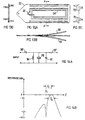
- Figure 1 shows an arrangement of an interrogator system in which an interrogator 1 containing a transmitter 2 generates an electromagnetic signal 3 which is transmitted via an interrogator antenna system 4 to an electronic label 5 containing a label receiving antenna 6.
- the label antenna 5 receives a proportion of the transmitted energy and through operation of a rectifier 7 generates a dc power supply for operation of a reply generation circuit 8 connected either to the label receiving antenna 6 or a separate label reply antenna 9 with the result that the an information bearing electromagnetic reply signal 10 is radiated by the label 5.
- a portion of a time-varying radio frequency signal transmitted by the label antenna 9 may enter the interrogator antenna 4 and in a signal separator 11 located within the interrogator 1 be separated from the signal transmitted by the interrogator 1 and passed to a receiver 12 wherein it is amplified, decoded and presented via a microcontroller 13 in digital or analog form to other systems such as a host computer or a system of sorting gates which make use of the information provided by the interrogator.
- operations of the reply generation circuit 8 may be controlled in time by an oscillator 14, the output of which may be used either directly or after reduction in frequency by a divider circuit 15 to control a code generator circuit 16 and a reply interval generator circuit 17.
- the code generator circuit 16 may control a modulator circuit 18 which may present a time-varying impedance varying in accordance with the modulation signal, either directly to the receiving antenna 6 or to the rectifier 7 or may apply a modulated reply carrier voltage to reply antenna 9.
- the code generator circuit may alternatively present an impedance directly varing in accord with the reply signal, either to the receiving antenna 6 or to the rectifier 7, or may present a reply signal directly to a separate reply antenna 9.
- the reply interval generator circuit 17 may control timing signals to the code generator circuit 16 or to the modulator circuit 18 so that the reply signal is radiated by the label 5 for only a portion of the time for which the label 5 is interrogated.
- Propagation of electromagnetic signals between the interrogator antenna system 4 and the label antenna 6 may be constrained to take place within a field confinement structure 19 which may be used to enhance coupling of energy between the interrogator antenna system 4 and the label antenna 6, and may also be used to diminish unwanted propagation of interrogator energy beyond the region desired for interrogation.
- the interrogator antenna system 4 may be connected to the interrogator 1 via an antenna re-configuration switch 20, either mechanical or electronic, which allows the nature of the interrogation field created by the interrogator antenna system 4 at the position of the label 5 to be changed in magnitude and direction.
- Such antenna re-configuration may be automatic over time or may be under control of the microcontroller 13 within the interrogator 1.
- the transmitter 2 may generate, in addition to the signals supplied to the interrogator antenna system 4, reference signals supplied to the receiver 12 and may also generate signals supplied to a field cancellation system 21 which may be placed externally to the field confinement system 19 or externally to the region occupied by the interrogator antenna system 4, and may serve to reduce net propagation of interrogation signals beyond the region desired for interrogation.
- the signals supplied to the field cancellation system 21 may be fixed in nature or may be varied under control of the microcontroller 13 which may receive signals from a field sensing system 22 which samples unwanted propagating signals in regions external to the interrogation region.
- the microcontroller 13 may perform in addition to those discussed various calculation and control functions such as functional testing of system components and may also participate in the reply decoding process.
- Figure 2 shows one preferred embodiment of a coded label.
- a label body 23 is constructed from a laminate of thin cardboard and plastics film.
- the coded label includes a label antenna 24 comprising an aluminium foil pattern embossed on to the plastics film, as does printed matching element 25.
- printed matching element 25 may carry aluminium conductors, and through-connections may be made by stamped holes filled with conductive adhesive.
- the printed matching element may be absent and is desirably so. Neither the antenna 24 or the matching element 25 require conductors of fine resolution nor positioning.
- the antenna 24 and matching element 25 are connected to the integrated microcircuit 26 via a pair of terminals, conductive adhesive being again the preferred mode of connection.
- an integrated matching element 27 preferably a capacitor, is connected in parallel with the antenna 24 and printed matching element 25 terminals.
- the system of antenna 24, printed matching element 25 and integrated matching element 27 may form a resonant circuit at the interrogation frequency so that coupling between the interrogator and the label is enhanced.
- the signal developed across the just mentioned resonant circuit is conveyed within the microcircuit 26 to an integrated rectifier 28 in which both rectifier diode and reservoir capacitor are manufactured as part of the microcircuit fabrication process.
- the voltage developed across a resevoir capacitor of the rectifier system is fed to a reply generation circuit 29 the output of which is conveyed either directly to the antenna system or is presented to the rectifier system.
- the operation of the rectifier circuit may be such as to draw from the label reply antenna non-sinusoidal currents, which may result in the emission from the label of signals at one or more of the harmonics of the interrogation frequency, these harmonic signals being detected by the interrogator.
- label antennae and printed matching elements are shown in Figures 3A and 3B.
- the label antenna is in the form of a electric dipole 30 again fabricated as stamped aluminium foil.
- the printed matching element takes the form of a rectangular spiral tuning inductor 31 connected in parallel with the antenna 30.
- the parallel combination is connected to the integrated microcircuit 26 via a pair of stamped aluminium foil conductors.
- the antenna consists of a magnetic dipole in the form of a large area spiral pattern loop 32 with only a small number of turns.
- the printed matching element takes the form of a tuning capacitor 33 fabricated as a pair of aluminium foil plates with the plastic film of the label body 23 as the dielectric. Necessary through-connections and connections to the microcircuit 26 are preferably made by stamped holes and conductive adhesive.
- the rectangular portion of the label antenna can be 50 by 80 mm with the magnetic dipole containing four turns each of strip width 0.8 mm and spacing 0.8 mm, and the printed tuning capacitor is absent.
- the reactance of the magnetic dipole antenna 32 is removed by an integrated matching element 29 consisting of a capacitor, preferably formed either with silicon dioxide dielectric between polysilicon layers or using gate oxide dielectric between a polysilicon layer and an implanted region of the substrate.
- the oscillating voltage developed across the antenna system is converted to a dc supply for the microcircuit 26 through the integrated rectifier diode 34 and integrated reservoir capacitor 35.
- the output of rectifier 34 is presented to an unmodulated variable load 36.
- the unmodulated variable load 36 operates under control of a voltage sensor 37 so that as the voltage developed by the rectifier 34 rises above the value for optimum circuit operation, a decreasing impedance is presented by the unmodulated variable load 36 to the rectifier 34.
- the result of the additional loading will reduce the quality factor of the resonant circuit formed by the magnetic dipole antenna and its matching element with the result that the label will be protected against incorrect functioning or damage from strong interrogation fields which are encountered by labels which pass with optimum orientation close to the interrogator antenna.
- interrogator fields of greater strength may be used, either fixed in time or adaptively varied, to elicit replies from badly positioned or orientated labels.
- the voltage developed by the rectifier 34 is also presented to and powers an integrated circuit oscillator 38.
- this oscillator will operate in the frequency range 180 kHz to 220 kHz, and will provide among other things a reply signal sub-carrier signal.
- An advantage of using within the label an integrated oscillator to control timing operations is that the high power consumption associated with circuits which derive their timing from counting down the relatively high interrogation frequency is avoided, and more of the power present in the label is available for generating the reply or for controlling essential processes which generate the reply by backscatter of a portion of the energy received by the label antenna.
- the output of integrated circuit oscillator 38 is fed to a bit rate divider 39 which in the preferred embodiment shown here will accomplish frequency division by a factor of 4.
- the output of the bit rate divider 39 is fed to a message interval circuit 40 which controls the operation of and receives information from a reply code generator circuit 41 containing a sixty-four bit reply code stored in a reply code memory.
- the information in the reply memory may be fixed in content at the time of manufacture, may be programmable at the time the label is brought into use, or may be re-programmed in operation, and may also contain a unique microcircuit serial number which may be made part of the reply or may be used for other purposes.
- the information in the reply code memory may be fed, in part, at the bit rate, to a modulator circuit 42 in which the reply information is modulated upon a reply sub-carrier provided by the integrated circuit oscillator 38.
- the relationship between the message interval circuit 40 and the reply code generator circuit 41 is in part as follows.
- the message interval circuit 40 asserts a Reply Code Generate signal which is passed to the reply code generator 41 which then issues, at the reply bit rate, four repetitions of the reply information stored in the reply code memory to the modulator, and also issues appropriate information to be defined below to the message interval circuit.
- the reply code generator 41 issues, at the reply bit rate, four repetitions of the reply information stored in the reply code memory to the modulator, and also issues appropriate information to be defined below to the message interval circuit.
- Other aspects of the interaction between the message interval circuit 40 and the reply code generator circuit 41 are discussed further below.
- the output of the reply code generator 41 is combined with the output of the integrated circuit oscillator 38 in the modulator 42 to accomplish differential phase shift keying of the reply sub-carrier frequency, a phase change in the output of the modulator occurring at the end of each four cycles of the reply sub-carrier whenever the output of the reply code generator 41 is a binary zero.
- the output of the modulator 42 together with the output of the voltage sensor 37 is applied to modulated variable load 43.
- This component presents to the power supply line a time-varying impedance which varies in accord with a signal from the phase modulator 42 and also varies with in amplitude with the signal derived from the voltage sensor 37.
- the result is that a time-varying loading is presented first to the rectifier 34 and is then presented by the rectifier 34 to the label antenna 32. It will there cause generation, through the mechanism of modulated backscatter described below, of a reply signal from the label.
- the reply signal may consist of modulated sidebands of the interrogator signal or modulated sidebands of a harmonic of the interrogator signal.
- variable impedance presented to the label antenna will provide that a portion of the available power received by the antenna will not be transmitted to its rectifier load, but will be reflected back into the antenna, wherefrom it will be re-radiated in a time varying manner.
- This time varying re-radiated signal will consist of sidebands of the original interrogation frequency, separated therefrom by a frequency difference equal to the frequency of the integrated circuit oscillator.
- the sub-carrier signal represented by those sidebands will be phase modulated with the reply signal information at the rate of one bit per four cycles of sub-carrier frequency.
- the amplitude of the impedance variation provided by the modulated variable load 43 is made dependent upon the output of the voltage sensor 37 so that, when an unmodulated variable load 43 presents a low impedance to rectifier 34, the relative level of unmodulated and modulated impedance may be approximately preserved, and the relative strength of the backscattered reply will not diminish.
- the advantage of the method of reply code generation discussed above is that the label may be operated without damage or malfunction over a wide dynamic range of interrogation signal.
- the Reply Code Generate signal is de-asserted and the generation of a reply signal by the label temporarily ceases.
- the message interval circuit receives data, either the reply code or a microcircuit serial number, from the reply code generator, and uses that data to initialize the state of a random number generator which is used to determine the number of reply bit periods which elapse before the Reply Code Generate signal is re-asserted and the reply signal is re-radiated by the label.
- the interval between reply periods is designed to be pseudo-randomly distributed between zero and 40 ms. That interval provides on the average an adequate time for replies from other labels simultaneously in the interrogation field to occur without interfering with the reply from the label under discussion. Even when such interference between replies does on one occasion occur, the differently seeded pseudo-random distribution of reply intervals within different labels will ensure that the probability of this interference continuing to occur will with time become vanishingly small.
- FIG. 4B An alternative preferred embodiment of the label is provided in Figure 4B.
- the reactance of the magnetic dipole antenna 32 is removed by the integrated tuning capacitor 33 placed within the integrated microcircuit 26.
- a power supply for the operation of the microcircuit is developed by the integrated rectifier diode 34 and integrated reservoir capacitor 35.
- an unmodulated variable load 36 operating under a control of voltage sensor 37 serves to keep the developed power supply within the microcircuit within acceptable levels in the face of large variations in strength of interrogator field.
- the power supply is again presented to a integrated circuit oscillator 38 which in this embodiment has an enhanced sensitivity of frequency to supply voltage and operates preferably in the range of 150 kHz to 250 kHz.
- the output of the integrated circuit oscillator 38 is passed to a bit rate divider 39 and a message interval circuit 40.
- the message interval circuit 40 simply consists of a dual counter which alternately issues a high signal for 256 of the reply bit periods, and a low signal for 4096 reply bit periods.
- the outputs of the bit rate divider 39 and the reply interval circuit 40 are both passed to a reply code generator 41 which performs functions similar to those described for Figure 4A, except that the information from the reply code generator 41 is not in this case conveyed to the reply interval circuit 40.
- the output of the reply code generator 41 is presented to the integrated circuit oscillator 38 wherein it accomplishes, at the bit rate, changes to the oscillator frequency in addition to the relatively slow changes accomplished by variations in supply voltage.
- the integrated circuit oscillator 38 is slowly varying with the microcircuit supply voltage and is in addition frequency modulated by the contents of a reply code memory within the reply code generator 41.
- the output of the integrated circuit oscillator 38 is presented, together with the output of the voltage sensor 37, to the modulated variable load 43 the operation of which is to generate through the mechanism of modulated backscatter, a reply code in the manner described in relation to Figure 4A.
- the voltage dependence of the integrated circuit oscillator within the microcircuit operates, together with the fact that the reply message is intermittently issued at intervals which vary inversely with the frequency of that oscillator, to ensure that whenever several labels are present within interrogation field, the natural variation between label circuits, together with variation in strength of interrogation field from one position to another within the interrogation environment, replies from different tags within the field will not permanently overlap.
- This feature of variation in the reply intervals between different labels may be enhanced by varying the power level of the interrogation field, as it is a property of most integrated circuit oscillators that the variation of oscillation frequency with power supply voltage increases as the supply voltage is reduced towards the threshold of oscillation.
- the probability of failure to read all labels passing through the scanned environment may be reduced to a negligible value.
- FIG. 5 The basic structure of yet another preferred embodiment of the label is shown in Figure 5.
- the receiving antenna 44 which received energy from the interrogation signal has its reactance removed by the combination of printed receiver matching element 45 and integrated receiver matching element 46.
- the voltage developed across that combination of elements is converted to a dc supply by an integrated rectifier 28 within the integrated microcircuit 26 and supplies power to the integrated reply generation circuit 29.
- the integrated reply generation circuit 29 develops a phase modulated reply signal at a frequency unrelated to that of the interrogation signal.
- the reply signal is presented to the reply antenna 47, which has its reactance removed by the integrated reply matching element 48 and printed reply matching element 49.
- the printed receiver matching element 45 may be absent.
- the reply frequency is preferably one for which low power integrated oscillator circuits and low cost printed antenna elements are both practicable. In this preferred embodiment a frequency in the vicinity of 2 MHz is suitable.
- the receiving magnetic dipole antenna 50 again consists of a rectangular coil of four turns of stamped aluminium foil of strictly 0.8 mm in separation 0.8 mm.
- the label is interrogated at a preferred interrogation frequency of 27 MHz.
- the required integrated receiver tuning capacitor 51 contained within the integrated microcircuit 26 is preferably realised with polysilicon electrodes separated by silicon dioxide dielectric.
- the integrated rectifier diode 34 is formed between a p type implanted layer and an n type substrate with the reservoir capacitor again employing either polysilicon electrodes and silicon dioxide dielectric or gate oxide dielectric with one polysilicon electrode and an implanted region of the substrate as another.
- An unmodulated variable load 36, operating under voltage sensor 37 performs functions corresponding to those described in relation to the preferred embodiments of figures 4A and 4B.
- the integrated circuit oscillator 38 will operate at a frequency of approximately 2 MHz and will be reduced in frequency in a bit rate divider 39 by a factor of 32 to produce a bit period of nominally 16 microseconds.
- the output of the bit rate divider is passed to the message interval circuit 40, which operates as described previously in relation to Figure 4A to provide an interval between replies effectively randomly distributed between zero and 40 ms.
- the output of the reply code generator 41 varies between low and high states and accomplishes frequency modulation of the integrated circuit oscillator 38.
- the output of the integrated circuit oscillator 38 remains undisturbed, other than to follow its normal variations with respect to power supply.
- the frequency modulated output of the integrated circuit oscillator 38 is presented directly to the transmitting magnetic dipole antenna 52 via additional output connections one of which is separate from those to the receiving magnetic dipole antenna 50.
- the reactance of the transmitting magnetic dipole 52 is removed by a combination of printed matching element 53 taking the form of an aluminium foil plastic dielectric capacitor and integrated tuning capacitor 54.
- Figure 7 Operations within the microcircuit of another preferred embodiment of the label shown in Figure 2 are shown in Figure 7.
- the sub-units 55, 57, 58, 63 and 64 are inactive and sub-units 32, 33, 34, 35, 36, 37, 38, 39, 40, 41, 43 function as described previously in relation to Figure 4B to generate a reply.
- the voltage fall detector 55 detects this condition and sends an Enter Program Mode signal 56 to program charge pump 57 and program control circuit 58.
- the program charge pump 57 Upon the receipt of this signal the program charge pump 57 becomes active and begins to generate through the mechanism of charge pumping a programming voltage higher than the normal circuit operating voltage provided by the rectifier diode 34 and reservoir capacitor 35, and supplies that voltage to the reply code generator 41 which in this embodiment contains at least part of the reply code in an electrically re-programmable memory.
- the program control circuit 58 sends a signal to the reply code generator 41 to prevent until the programming process is complete the generation of the reply code.
- the interrogation signal must be modulated in amplitude with a depth of at least 20% and at a bit rate corresponding to the bit rate of the reply previously issued by the label.
- the interrogator power level is predictively adjusted to bring that bit rate to the nominal 50 kbits per second for this design of label.
- the form of modulation of the interrogator power is pulse width modulation with a binary one being signalled by a high power level for a period of 15 microseconds followed by a low power level (less than 80% of full power) for a period of 5 microseconds, while a binary zero is signalled by a low power level (less than 80% of full power) for a period of 15 microseconds followed by a high power level for a period of 5 microseconds.
- this form of modulation is detected by the voltage fall detector 55, and is passed to the program control circuit 58. That circuit records the first 64 binary digits signalled to the label and interprets them as a programming mode key.
- the interpretation of those digits employs the principle of feedback shift register encoding using the reply code as a key, so that for each label the correct value of the key depends upon its programmed contents and is calculated in the interrogator from the just received reply before it is issued.
- the label interprets the next portion of the programming bit stream as data to be programmed into reply memory. Providing the conditions relating to Program Lock and Program Enable bits described below are satisfied, that data is then with the aid of Programming in Progress Signal 59, Write Data Signal 60, Write Enable Signal 61 entered into the reply code memory of reply code generator 41, taking a time appropriate to the programming speed of the memory. Upon the completion of the entry of the programmed data the reply code generation functions of the label are restored, and the interrogator checks that correct programming has taken place.
- the operations described above will only occur when two bits of the reply code memory, known as the Program Enable Bit and the Program Lock Bit, are in the appropriate states.
- the Program Enable Bit which can when the Auxiliary Programming Signal to be described below is applied, be both raised and lowered by the programming process described above, must be in a high state
- the Programming Lock Bit which when the Auxiliary Programming Signal described below is applied can be raised by the programming process described above but once raised cannot be lowered by any means, must be in a low state.
- a second electromagnetically coupled signal For the Auxiliary Programming Signal to be asserted on the label a second electromagnetically coupled signal must be applied to the label antenna.
- This auxiliary signal is applied via a carrier at a frequency of approximately 500 MHz, and is applied to the label in a programming chamber which may take the form of a closed metal container or a waveguide beyond cut-off.
- the second electromagnetically coupled signal enters the label via the same terminal pair as the interrogation signal.
- Figure 8 shows a preferred embodiment of an object identification system containing a field confinement structure and a field cancellation structure.
- baggage items 65 with attached electronic labels 5 are placed on non-metallic conveyor 66 through a rectangular metallic tunnel 67 which serves as the field confinement structure.
- the tunnel 67 has an interior width of 900 millimetres, an interior height of 1 metre, and a length of 2 metres, and interrogation takes place at a frequency of 27MHz, at which frequency the electromagnetic wavelength is much greater than both aperture dimensions of the tunnel 67.
- the interrogation field is created by rectangular bar antennae approximately 100 millimetres in square cross section, attached to each side wall and with a 20 millimetre gap at the centre providing a feed point for that antenna. From the feed point a coaxial line passes through the interior of one bar to the outside wall of the structure, thus permitting shielded connection of that antenna to the iterrogator 1.
- the fields created by the antennae are substantially magnetic and follow a path surrounding the antenna bars in closed loops. A portion of the field extends into the interior section of the tunnel 67 with the return flux path being provided by the metallic wall antenna housings 68 which provide a vertical expansion of the tunnel 67 cross section in the vicinity of its centre.
- the interrogator 1 has connections also to field cancellation antennae 21 placed close to each end of the tunnel mouth.
- the field cancellation antennae 21 are capable of radiating both vertically and horizontally polarized electromagnetic fields, the radiation being adjusted to cancel in the far field region of the residual radiation emerging from each end of the tunnel mouth.
- the interrogator 1 shown in Figure 8 may contain a number of independent transmitter, receiver and reply decoder systems, connected separately to interrogator antennas 68, the outputs of the said decoder systems being combined in one of the decoders or in an overall system controller within the interrogator so that for each correctly decoded label a single report of its decoded reply is provided to the sorting gates or host computer.
- the bars are increased in width to 300 mm and are driven in phase, or in quadrature.
- This shaping of the antenna field has the advantage that replies form tags in particular orientations are confined to short intervals of time as a label passes through the antenna region with the result that the order of entry of labels into the interrogation region may be inferred with increased accuracy compared with field generation systems creating spatially more uniform fields.
- Figures 9A-9D An alternative preferred embodiment of the field confinement structure and interrogation field antenna structure is illustrated in Figures 9A-9D.
- Figure 9A shows a sectional view on BB of Figure 9B and Figure 9B shows a sectional view on AA of Figure 9A.
- Figure 9C shows a sectional view on CC of Figure 9A and Figure 9C shows a sectional view on DD of Figure 9A.
- a waveguide beyond cut-off of dimensions similar to that discussed in Figure 8 for an operating frequency of approximately 27 MHz is again used.
- the interrogation field creation antennae take the form of ferrite bars 69 excited by ferrite antenna windings 70 and placed in shallow chambers 71 exterior to the tunnel walls and of length a little less than the height of the tunnel, and communicating therewith through rectangular apertures 72 which provide an entry for the magnetic flux within the ferrite bars 69 generated by the antenna excitation system.
- the confinement of the interrogation fields substantially to the region of the tunnel is achieved in part by again exploiting the properties of electromagnetic field distributions in waveguides beyond cut-off and in part by the insertion of current inhibiting chokes 73 in series with the tunnel walls between the region occupied by the interrogation antenna structure and the tunnel openings.
- the chokes illustrated take the form of a re-entrant coaxial lines, short circuited at one end and of total length one quarter of a wave length so that at the aperture 74 at which they connect to the interrupted tunnel walls an open circuit is presented.
- chokes 73 serve to inhibit the passage of wall currents across the gap and thus aid in the confinement of the interrogation field to the central region of the tunnel.
- FIG. 10 A preferred embodiment of yet another type of interrogation field creation and cancellation structure is illustrated in Figure 10.
- baggage items 65 carrying electronic labels 5 enter on a conveyor 66 which passes through a pair of single-turn portal interrogation antennae 75 in which reactance is removed by a number of series tuning capacitors 76 disposed at intervals around the circumference of the loops.
- the loop antennae are spaced in the direction of the conveyor by distance approximately equal to the width and are excited by the interrogator 1 so that currents 77 flow in opposite directions in the two loops.
- On top of the interrogator smaller but similarly oriented field cancellation antennae 78 are mounted.
- the field created by the interrogation antenna system is substantially quadrupole in nature with a maximum logitudinal component in the centre of each loop and a null field half way between them.
- the disposition of currents and the positions of the antennae are such as to minimize radiation to the far field. Such radiation as does occur is substantially cancelled by suitably phased additional currents which flow in the field cancellation antennae 78 mounted on the interrogator 1 or elsewhere if desired.
- the field cancellation antennae are sufficiently small for their own near fields not to significantly reduce the interrogation field at the label position.
- the advantages of this form of field creation and stray field cancellation are: economy of space occupied by and economy in cost of manufacture of an interrogation installation; reduction in radiation of interrogation energy to far fields as a result firstly of the use of distributed series tuning capacitors, secondly as a result of the magnetic quadrupole nature of the field creation structure, and thirdly as a result of the stray field cancellation system, so that type approval of an interrogation installation may be more easily obtained; as a result of the distributed capacitance of the tuning system a reduction of both dangerous voltages and unwanted electric fields in the interrogation region; and as a consequence of the interrogation field distribution the obtaining of two interrogation opportunities for one pass of a label through the interrogation antenna structure.
- the field shaping which results from overlap of the antenna fields and the relative amplitude and phasing of the antenna currents to produce a field null between the loops offers the advantage of more accurate inference of relative label position as labels pass through the interrogation region.
- FIG. 11 A block diagram of a preferred embodiment of an interrogator system is provided in Figure 11.
- the interrogation signal is generated by a local oscillator 79, increased in amplitude in a transmitter signal amplifier 80 and passed through signal separator 11 to interrogator antenna system 4.
- the reply signal from the labels is received by the same interrogator antenna system and separated by signal separator 11 and passed via receiver filter 81 to balanced modulator 82.
- the receiver filter provides very large attenuation, of the order of 60 dB, at the interrogation frequency while providing a passband 100 kHz wide situated 200 kHz above the interrogation frequency for the reply signal.
- receiver filter with these properties are that: reduction in receiver sensitivity through saturation of the down-converting mixer is avoided; the introduction of interrogator signal phase noise into the receiver path is reduced; the influence of environmental noise in the receiver is reduced; and positional nulls in the label reply which result when double sideband homodyne reception is used are eliminated.
- the balanced modulator 82 also receives a signal from the local oscillator 79 to effect down-conversion of the reply signal to a more convenient amplifying frequency.
- the output signal of balanced modulator 82 is passed to an amplitude detector system 83, the output of which enters microcontroller 13 to serve as an indication of whether replies have been obtained or some adjustment to interrogator power is required.
- This adaptive adjustment of interrogator power has the advantage of eliciting replies from unfavourably oriented or positioned labels.
- the output of balanced modulator 82 is also passed to a low frequency band pass amplitude limiting amplifier 84 which provides amplification in the region of the reply sub-carrier, and also provides suppression of small signals.
- the advantage of using an amplitude limiting amplifier, and frequency or phase modulation in the encoding of the label reply, are that when more than one label has responded only the strongest supply is significantly present at its output, and that the preferably phase or frequency or modulated reply signals are presented at a suitable amplitude to signal sampler 85.
- the signal sampler 85 takes limited resolution samples at a frequency significantly greater than the reply sub-carrier frequency so that a digital representation of the reply signal is passed to microcontroller 13. This method of operation offers advantages in that before the frequency or phase encoded reply information is extracted, decoding algorithms within microcontroller 13 can detect and compensate for time warping of the reply signal sub-carrier frequency which can occur as labels move through the interrogation field which varies in strength from position to position.
- the microcontroller 13 also controls the gain of a cancellation signal amplifier 86 of which the input signal is the derived from the local oscillator 79 and the output signal is conveyed to field cancellation antennae 87 to give the advantage of minimisation of stray radiation which escapes the field confinement system.
- the level of the cancellation field is determined by the microcontroller 13 which receives information from stray field sensing antennae 21 via stray field sensing amplifiers 88 and stray field sensing detectors 89.
- the microcontroller 13 may also control an antenna re-configuration switch which can place the excitations of antennae on opposite sides of the tunnel in phase, in anti-phase or in quadrature to provide the advantage of minimisation of weak field positions and unfavourable label orientations within the structure.
- the receiver filter 81 provides its passband 200 kHz above or below the second harmonic of the interrogation frequency, and the balanced modulator 82 is fed with a local oscillator signal at the second harmonic of the interrogation signal.
- An advantage of providing for reply detection in the band surrounding an harmonic of the interrogation signal is that harmonic energy and phase noise of the transmitter signal, which in homodyne receivers present a limit to system sensitivity, may in this elevated reply passband be easily removed from the transmitter signal by low cost filter circuits.
- a further advantage of the use of a reply passband near an harmonic of the interrogation frequency is that local scattering systems such as electrically powered machinery which can interact readily with the interrogation signal to produce at sidebands of the interrogation frequency intefering signals which can compete with the label reply, do not as readily produce interfering signals at sidebands an harmonic of the interrogation frequency, and label replies can be detected in the presence of strong local scatterers.
- FIG. 12 A block diagram of another preferred embodiment of an interrogator system is provided in Figure 12.
- the interrogation signal is generated by a transmitter master oscillator 90, increased in amplitude in a transmitter signal amplifier 80 and passed through frequency selective signal separator 91 to interrogator antenna system 4.
- the reply signal from the labels is received by the same interrogator antenna system and separated by signal separator 91 and passed via receiver filter 81 to balanced modulator 82. While no longer requiring a sharp notch at the interrogation frequency in its response, this receiver filter 81 has the task of sharply rejecting signals at the interrogation frequency while providing an appropriate passband for the reply signal.
- the balanced modulator 82 also receives a signal from a receiver local oscillator 92 to effect down-conversion of the reply signal to a more convenient amplifying frequency.
- the output signal to the balanced modulator 82 is passed to an amplitude detector system 83 the output of which enters the microcontroller 13 to serve as an indication of whether replies have been obtained or some adjustment to the interrogator power is required.
- the output of the balanced modulator 82 is also passed to a low frequency band pass amplitude limiting amplifier 84 which provides amplification in the region of the reply frequency base band and also suppression of small signals to ensure that when more than one label has responded only the strongest supply is significantly present at its output, and also to present the preferably frequency modulated reply signals at a suitable amplitude to the signal sampler 85.
- This component takes limited resolution samples at a frequency significantly greater than the reply sub-carrier frequency so that a digital representation of the reply signal is passed to the microcontroller 13. This method of operation offers the same advantages as were discussed in relation to Figure 11.
- the microcontroller 13 also controls the gain of a cancellation signal amplifier 86, the input signal of which is the derived from master oscillator 90 and the output signal is conveyed to field cancellation antennae 87 whose purpose is to cancel stray radiation which escapes the field confinement system.
- the level of the cancellation field is determined by the microcontroller 13 which receives information from stray field sensing antennae 21 via stray field sensing amplifiers 88 and stray field sensing detectors 89.
- Figures 13A-13D show plan, side elevation and end elevation views of the label.
- Figure 13D shows a sectional view on AA of Figure 13A.
- the label consists of a plastic label body 23 to which is attached a stamped metal foil antenna 24 connected to the integrated microcircuit 26.
- circuit diagram and frequency response when placed between fifty ohm source and load impedances of a receiver filter suitable for use in the interrogator defined in Figure 11 and operating at an interrogation frequency of 27 MHz are shown in Figures 14A and 14B respectively.
- the circuit shown in Figure 14A consists of a piezoelectric crystal 94 with its series mode resonance set to the interrogation frequency f i , in this case 27 MHz, with the combination of the crystal self capacitance (not explicitly shown in the circuit) and the added capacitance 95 being tuned by inductor 96 to a frequency an amount f c above the series mode resonance, where f c is the reply frequency sub-carrier.
- the series capacitors 97 accomplish impedance transformation of the resonant circuit formed by the inductor 96, crystal capacitance and added capacitance 95 so that, in conjunction with the source and load impedances, between which the circuit is placed, the 3 dB bandwidth of the passband provided for the reply signal upper sideband is established to be 100 kHz while the depth of the notch established at the interrogation frequency f i is at least 60 dB.
Claims (18)
- Identifizierungs- und Telemetriesystem mit
einem Abfrager (1), der einen Sender (2) für das Erzeugen eines Abfragesignals (3) bei einer Abfragesignal-Frequenz und einen Empfänger für die Erfassung und die Dekodierung eines Antwortsignals beinhaltet;
einer Abfragefeld-Erzeugungs- und Begrenzungs-Vorrichtung (19), umfassend eine Sendeantenne (4), die mit dem Sender (2) verbunden ist, um aus dem Abfragesignal ein elektromagnetisches Abfragefeld zu erzeugen, durch welches ein Objekt hindurchtreten kann, das ein Kode-Antwort-Etikett (5) aufweist,
wobei das Kode-Antwort-Etikett (5) eine Etiketten-Empfangsantenne (6) für das Empfangen eines Etikettenabfragesignals aus dem Abfragefeld (3), eine Einrichtung zur Erzeugung eines Etikettenantwortsignals und eine Einrichtung zur Erzeugung eines elektromagnetischen Antwortfeldes (10) aus dem Etikettenantwortsignal umfasst;
einer Empfängerantenne (4), die mit dem Empfänger (12) verbunden ist, für das Empfangen eines Antwortsignals aus dem elektromagnetischen Etikettenantwort-Feld;
wobei die Feld-Erzeugungs- und Begrenzungs-Vorrichtung (19) bei der Abfragesignal-Frequenz einen Wellenleiter umfasst, der unterhalb seiner Abschneidefrequenz zum Begrenzen des elektromagnetischen Abfragefelds arbeitet. - Identifizierungs- und Telemetriesystem nach Anspruch 1, wobei das Kode-Antwort-Etikett (5) einen Gleichrichter (7) aufweist, der eine Diode und einen Speicherkondensator für die Umwandlung eines Teils der Energie, welche als Wechselspannung über das Etikettenabfragesignal (3) geliefert wird, in Gleichstrom umfasst.
- Identifizierungs- und Telemetriesystem nach Anspruch 1, wobei die Feld-Erzeugungs- und Begrenzungs-Vorrichtung (19) ein magnetisch permeables Material in einem metallisch begrenzten Rückkehrflusspfad für die magnetische Komponente des Abfragefelds aufweist.
- Identifizierungs- und Telemetriesystem nach Anspruch 1, umfassend einen Abfragebereich, in und aus welchem das Objekt treten kann, wobei die Feld-Erzeugungs- und Begrenzungs-Vorrichtung (19) mindestens eine metallische Leiterbahn (67) umfasst, die den Abfragebereich umgibt, und wobei eine durch die Leiterbahn gebildete Öffnung, durch welche das Objekt einen Einlass zu dem Abfragebereich erhält oder aus diesem austritt, Abmessungen aufweist, die kleiner als die Hälfte der elektromagnetischen Wellenlänge der Abfragefrequenz sind.
- Identifizierungs- und Telemetriesystem nach Anspruch 4, wobei die Feld-Erzeugungs- und Begrenzungs-Vorrichtung (19) eine Metallwand-Röhre umfasst, die an der Öffnung befestigt ist, um den Wellenleiter zu bilden.
- Identifizierungs- und Telemetriesystem nach Anspruch 1, wobei die Feld-Erzeugungs- und Begrenzungs-Vorrichtung (19) Objekt-Eingangs- und Ausgangsbereiche aufweist, und wobei Drosselmittel (73), die das Fließen von Wandströmen verhindern, in den Objekt-Eingangs- und Ausgangsbereichen angeordnet sind.
- Identifzierungs- und Telemetriesystem nach Anspruch 1, wobei die Feld-Erzeugungs- und Begrenzungs-Vorrichtung (19) eine Metallwand-Röhre umfasst, die Querschnitts-Abmessungen aufweist, die kleiner als die Hälfte der Wellenlänge der Abfrage-Frequenz sind.
- Identifizierungs- und Telemetriesystem nach Anspruch 1, wobei die Feld-Erzeugungs- und Begrenzungs-Vorrichtung (19) Objekt-Eingangs- und Ausgangsbereiche aufweist, und wobei die Objekt-Eingangs- und Ausgangsbereiche bei der Abfragesignal-Frequenz den Wellenleiter bilden, der unterhalb seiner Abschneidefrequenz arbeitet.
- Identifizierungs- und Telemetriesystem nach Anspruch 8, wobei die Feld-Erzeugungs- und Begrenzungs-Vorrichtung (19) Objekt-Eingangs- und Ausgangsbereiche aufweist, und wobei die Drosselmittel (73), die das Fließen von Wandströmen verhindern, in den Objekt-Eingangs- und Ausgangsbereichen angeordnet sind.
- Identifizierungs- und Telemetriesystem nach Anspruch 1, wobei die Feld-Erzeugungs-Vorrichtung Stäbe oder Stangen (69) aus einem metallisch permeablen Material aufweist, die in einer metallischen Kammer oder an Innenwänden einer metallischen Röhre angeordnet sind.
- Identifizierungs- und Telemetriesystem nach Anspruch 1, wobei die Abfragesignal-Frequenz einen gleichzeitigen Einsatz einer monolithischen integrierten Gleichrichterdiode (34) und eines monolithisch integrierten Speicherkondensators (35) gestattet.
- Identifizierungs- und Telemetriesystem nach Anspruch 11, wobei die Feld-Erzeugungs- und Begrenzungs-Vorrichtung (19) Objekt-Eingangs- und Ausgangsbereiche aufweist, und wobei die Objekt-Eingangs- und Ausgangsbereiche bei der Abfragesignal-Frequenz den Wellenleiter bilden, der unterhalb seiner Abschneidefrequenz arbeitet.
- Identifizierungs- und Telemetriesystem nach Anspruch 1, umfassend ein Streufeld-Auslöschmittel (87), das mit dem Abfrager verbunden ist, das von dem Abfrager ein Signal mit der Abfragefrequenz empfängt und in einem Bereich außerhalb der Abfragefeld-Erzeugungs- und Begrenzungs-Vorrichtung (19) ein elektromagnetisches Auslöschfeld erzeugt, um in diesem Bereich das elektromagnetische Streufeld auszulöschen, welches von der Feld-Erzeugungs- und Begrenzungs-Vorrichtung hervorgeht, und wobei die dem Streufeld-Auslöschmittel (87) gelieferten Signale adaptiv eingestellt werden, um das aus der Feld-Erzeugungs-Vorrichtung tretende elektromagnetische Streufeld zu minimieren.
- Identifizierungs- und Telemetriesystem nach Anspruch 1, wobei die Abfragefeld-Erzeugungs- und Begrenzungs-Vorrichtung (19) eine Vielzahl von Sendeantennen umfasst und die Signale in den Sendeantennen in Amplitude und Phase eingestellt werden, um die elektromagnetischen Streufelder zu reduzieren, die in einem Bereich außerhalb demjenigen erzeugt werden, in welchem die Abfrage eines Etiketts (5) beabsichtigt ist, zu geschehen.
- Identifizierungs- und Telemetriesystem nach Anspruch 1, wobei das Abfragefeld durch eine Vielzahl von Sendeantennen (4) bereitgestellt wird, die überlappende und störende Felder in der Feld-Erzeugungs-und Begrenzungs-Vorrichtung erzeugen.
- Identifizierungs- und Telemetriesystem nach Anspruch 4, wobei die mindestens eine metallische Leiterbahn (67) eine Lücke aufweist, die ein Paar von Anschlüssen für die Verbindung mit dem Sender (2) liefert.
- Identifizierungs- und Telemetriesystem nach Anspruch 4, wobei die mindestens eine metallische Leiterbahn (67) eine Vielzahl von Lücken aufweist, über welche eine Vielzahl Serien-Resonanz-Kondensatoren (76) angeschlossen sind.
- Identifizierungs- und Telemetriesystem nach Anspruch 1, wobei das Abfragefeld durch ein Paar von Schleifenantennen (75) geliefert wird, die auf einer gemeinsamen Achse konfiguriert sind und Ströme (77) mit entgegengesetzten Phasen bei der Abfragesignal-Frequenz tragen.
Applications Claiming Priority (4)
| Application Number | Priority Date | Filing Date | Title |
|---|---|---|---|
| AUPK538691 | 1991-04-03 | ||
| AUPK538691 | 1991-04-03 | ||
| AUPK5386/91 | 1991-04-03 | ||
| EP92907816A EP0578701B1 (de) | 1991-04-03 | 1992-04-03 | Warensortiersystem |
Related Parent Applications (2)
| Application Number | Title | Priority Date | Filing Date |
|---|---|---|---|
| EP92907816A Division EP0578701B1 (de) | 1991-04-03 | 1992-04-03 | Warensortiersystem |
| EP92907816.0 Division | 1992-10-22 |
Publications (3)
| Publication Number | Publication Date |
|---|---|
| EP0918308A2 EP0918308A2 (de) | 1999-05-26 |
| EP0918308A3 EP0918308A3 (de) | 2000-10-04 |
| EP0918308B1 true EP0918308B1 (de) | 2005-12-14 |
Family
ID=3775310
Family Applications (2)
| Application Number | Title | Priority Date | Filing Date |
|---|---|---|---|
| EP92907816A Expired - Lifetime EP0578701B1 (de) | 1991-04-03 | 1992-04-03 | Warensortiersystem |
| EP99200019A Expired - Lifetime EP0918308B1 (de) | 1991-04-03 | 1992-04-03 | Artikelsortiersystem |
Family Applications Before (1)
| Application Number | Title | Priority Date | Filing Date |
|---|---|---|---|
| EP92907816A Expired - Lifetime EP0578701B1 (de) | 1991-04-03 | 1992-04-03 | Warensortiersystem |
Country Status (6)
| Country | Link |
|---|---|
| US (2) | US5523749A (de) |
| EP (2) | EP0578701B1 (de) |
| AT (2) | ATE185914T1 (de) |
| DE (2) | DE69230171T2 (de) |
| ES (1) | ES2252911T3 (de) |
| WO (1) | WO1992017866A1 (de) |
Families Citing this family (120)
| Publication number | Priority date | Publication date | Assignee | Title |
|---|---|---|---|---|
| ATE185914T1 (de) * | 1991-04-03 | 1999-11-15 | Integrated Silicon Design Pty | Warensortiersystem |
| US7158031B2 (en) | 1992-08-12 | 2007-01-02 | Micron Technology, Inc. | Thin, flexible, RFID label and system for use |
| US6097301A (en) * | 1996-04-04 | 2000-08-01 | Micron Communications, Inc. | RF identification system with restricted range |
| US20050040961A1 (en) * | 1995-04-11 | 2005-02-24 | Tuttle John R. | RF identification system with restricted range |
| JP3305843B2 (ja) * | 1993-12-20 | 2002-07-24 | 株式会社東芝 | 半導体装置 |
| AUPM690494A0 (en) * | 1994-07-18 | 1994-08-11 | Magellan Corporation (Australia) Pty Ltd | Attenuator |
| JP2853965B2 (ja) * | 1994-07-26 | 1999-02-03 | センサーテクノス株式会社 | 食堂の精算装置 |
| DE4431604A1 (de) * | 1994-09-05 | 1996-03-07 | Siemens Ag | Schaltungsanordnung mit einem Chipkartenmodul und einer damit verbundenen Spule |
| GB9502907D0 (en) * | 1995-02-15 | 1995-04-05 | Int Computers Ltd | Electronic identification system |
| US7123129B1 (en) * | 1995-08-14 | 2006-10-17 | Intermec Ip Corp. | Modulation of the resonant frequency of a circuit using an energy field |
| US7002475B2 (en) * | 1997-12-31 | 2006-02-21 | Intermec Ip Corp. | Combination radio frequency identification transponder (RFID tag) and magnetic electronic article surveillance (EAS) tag |
| US6400274B1 (en) * | 1995-08-31 | 2002-06-04 | Intermec Ip Corp. | High-performance mobile power antennas |
| US7511621B1 (en) | 1995-08-31 | 2009-03-31 | Intermec Ip Corp. | High-performance mobile power antennas |
| FR2738370B1 (fr) * | 1995-09-06 | 1997-11-07 | France Telecom | Installation pour l'echange d'informations a distance entre un objet portatif passif et une station, objet et station correspondants |
| FR2747250B1 (fr) * | 1996-04-03 | 1998-06-26 | Bouvier Jacky | Procede d'echange d'informations a distance entre un objet electronique portatif, tel qu'une carte a memoire, et un terminal, et objet portatif correspondant |
| AU709985B2 (en) * | 1996-06-19 | 1999-09-09 | Gemplus | Enhanced range transponder system |
| AUPO055296A0 (en) * | 1996-06-19 | 1996-07-11 | Integrated Silicon Design Pty Ltd | Enhanced range transponder system |
| DE19633923A1 (de) * | 1996-08-22 | 1998-02-26 | Siemens Ag | Chipkarte mit einer Induktionsspule und Verfahren zu ihrer Herstellung |
| US6362737B1 (en) * | 1998-06-02 | 2002-03-26 | Rf Code, Inc. | Object Identification system with adaptive transceivers and methods of operation |
| US6222452B1 (en) * | 1996-12-16 | 2001-04-24 | Confidence International Ab | Electronic identification tag |
| US6104333A (en) * | 1996-12-19 | 2000-08-15 | Micron Technology, Inc. | Methods of processing wireless communication, methods of processing radio frequency communication, and related systems |
| US6084530A (en) * | 1996-12-30 | 2000-07-04 | Lucent Technologies Inc. | Modulated backscatter sensor system |
| US6046683A (en) * | 1996-12-31 | 2000-04-04 | Lucent Technologies Inc. | Modulated backscatter location system |
| US5952922A (en) * | 1996-12-31 | 1999-09-14 | Lucent Technologies Inc. | In-building modulated backscatter system |
| US6456668B1 (en) | 1996-12-31 | 2002-09-24 | Lucent Technologies Inc. | QPSK modulated backscatter system |
| US5784686A (en) * | 1996-12-31 | 1998-07-21 | Lucent Technologies Inc. | IQ combiner technology in modulated backscatter system |
| US6130623A (en) * | 1996-12-31 | 2000-10-10 | Lucent Technologies Inc. | Encryption for modulated backscatter systems |
| US6184841B1 (en) | 1996-12-31 | 2001-02-06 | Lucent Technologies Inc. | Antenna array in an RFID system |
| FR2760998B1 (fr) * | 1997-03-21 | 1999-05-21 | Equisecurite Sa | Procede d'inclusion d'une etiquette electronique dans un objet realise en plastique, au moment de la fabrication de l'objet |
| US6980085B1 (en) | 1997-08-18 | 2005-12-27 | Micron Technology, Inc. | Wireless communication devices and methods of forming and operating the same |
| US6339385B1 (en) * | 1997-08-20 | 2002-01-15 | Micron Technology, Inc. | Electronic communication devices, methods of forming electrical communication devices, and communication methods |
| GB9727042D0 (en) * | 1997-12-22 | 1998-02-18 | Advanced Technology Communicat | Tag and detection system |
| GB2335573B (en) | 1998-03-18 | 2000-03-15 | Univ Singapore | An RF transponder identification system and protocol |
| US6185479B1 (en) * | 1998-04-15 | 2001-02-06 | John F. Cirrone | Article sorting system |
| US6107921A (en) | 1998-04-16 | 2000-08-22 | Motorola, Inc. | Conveyor bed with openings for capacitive coupled readers |
| US6570541B2 (en) | 1998-05-18 | 2003-05-27 | Db Tag, Inc. | Systems and methods for wirelessly projecting power using multiple in-phase current loops |
| US6388628B1 (en) * | 1998-05-18 | 2002-05-14 | Db Tag, Inc. | Systems and methods for wirelessly projecting power using in-phase current loops |
| AUPP473898A0 (en) * | 1998-07-20 | 1998-08-13 | Integrated Silicon Design Pty Ltd | Metal screened electronic labelling system |
| JP3916328B2 (ja) * | 1998-07-27 | 2007-05-16 | ローム株式会社 | 非接触通信システム |
| EP1862982B1 (de) | 1998-08-14 | 2014-11-19 | 3M Innovative Properties Company | Verfahren zur Abfrage einer Verpackung mit RFID-Etikett |
| IL127569A0 (en) | 1998-09-16 | 1999-10-28 | Comsense Technologies Ltd | Interactive toys |
| AU6245899A (en) * | 1998-09-11 | 2000-04-03 | Motorola, Inc. | Generation of electrostatic voltage potentials for rfid/eas using piezoelectric crystals |
| US8228193B1 (en) * | 1998-09-14 | 2012-07-24 | Tuemer Tuemay O | Tag having a semiconductor chip and method of attachment to article |
| US6607136B1 (en) | 1998-09-16 | 2003-08-19 | Beepcard Inc. | Physical presence digital authentication system |
| EP1116155A2 (de) | 1998-10-02 | 2001-07-18 | Comsense Technologies Ltd. | Karte zur interaktion mit einem computer |
| DE19850353C1 (de) * | 1998-11-02 | 2000-03-16 | David Finn | Identifikationslabel sowie Verfahren zur Herstellung eines Indentifikationslabels |
| NL1010457C2 (nl) * | 1998-11-03 | 2000-05-04 | Nedap Nv | Grote lusantennes. |
| JP2000295027A (ja) * | 1999-02-01 | 2000-10-20 | Supersensor Pty Ltd | 電子識別システムに用いるハイブリッドアンテナ装置 |
| DE29905840U1 (de) * | 1999-03-30 | 1999-06-10 | Moba Mobile Automation Gmbh | Müllsackidentifikationssystem |
| JP3687459B2 (ja) * | 1999-06-29 | 2005-08-24 | ソニーケミカル株式会社 | Icカード |
| US6388630B1 (en) * | 1999-07-22 | 2002-05-14 | Supersensor (Proprietary) Limited | Waveguide for transmitting RF energy through an RF barrier |
| JP2001043336A (ja) * | 1999-07-29 | 2001-02-16 | Sony Chem Corp | Icカード |
| US6714121B1 (en) | 1999-08-09 | 2004-03-30 | Micron Technology, Inc. | RFID material tracking method and apparatus |
| US8019609B2 (en) | 1999-10-04 | 2011-09-13 | Dialware Inc. | Sonic/ultrasonic authentication method |
| US7280970B2 (en) * | 1999-10-04 | 2007-10-09 | Beepcard Ltd. | Sonic/ultrasonic authentication device |
| DE60023561T2 (de) * | 1999-12-03 | 2006-07-27 | Tagsys S.A. | Elektronisches etikettenlesesystem |
| US6960984B1 (en) * | 1999-12-08 | 2005-11-01 | University Of North Carolina | Methods and systems for reactively compensating magnetic current loops |
| FR2802738A1 (fr) * | 1999-12-15 | 2001-06-22 | Circe | Dispositif de lecture de transpondeur |
| US6522308B1 (en) * | 2000-01-03 | 2003-02-18 | Ask S.A. | Variable capacitance coupling antenna |
| JP3885922B2 (ja) * | 2000-03-07 | 2007-02-28 | 株式会社ルネサステクノロジ | 半導体チップとそれを用いたicカード及びrfid |
| US6369710B1 (en) | 2000-03-27 | 2002-04-09 | Lucent Technologies Inc. | Wireless security system |
| US7180402B2 (en) * | 2000-06-06 | 2007-02-20 | Battelle Memorial Institute K1-53 | Phase modulation in RF tag |
| EP1170695B1 (de) * | 2000-07-04 | 2008-12-03 | Texas Instruments Deutschland Gmbh | Abgleichschaltung zur Abgleichung von folienförmigen Antennen |
| US6714136B1 (en) * | 2000-08-14 | 2004-03-30 | Computime, Ltd. | Alarm clock with remote control function |
| JP2004536361A (ja) * | 2000-10-10 | 2004-12-02 | エスコート・メモリー・システムズ | モジュラーrfidアンテナシステム |
| DE10052444A1 (de) * | 2000-10-23 | 2002-05-08 | Avery Dennison Corp Pasadena | Verwendung eines RFID-Etikettes zum Kennzeichnen eines zu transportierenden Gegenstandes hinsichtlich seines Zielorts sowie System, Verfahren, Drucker und Anhänger hierfür |
| FR2817692B1 (fr) * | 2000-12-01 | 2003-10-03 | Gemplus Card Int | Procede et systemes de controle de reproduction de documents |
| US6946951B2 (en) | 2000-12-29 | 2005-09-20 | Tagsys Australia Pty Ltd. | System and method for interrogating electronic labels |
| US6715089B2 (en) * | 2001-01-22 | 2004-03-30 | Ati International Srl | Reducing power consumption by estimating engine load and reducing engine clock speed |
| US9219708B2 (en) | 2001-03-22 | 2015-12-22 | DialwareInc. | Method and system for remotely authenticating identification devices |
| US7377445B1 (en) | 2001-05-31 | 2008-05-27 | Alien Technology Corporation | Integrated circuits with persistent data storage |
| US6942155B1 (en) * | 2001-05-31 | 2005-09-13 | Alien Technology Corporation | Integrated circuits with persistent data storage |
| ITPD20010217A1 (it) * | 2001-09-11 | 2003-03-11 | Eds Te Ma Srl | Metodo di identificazione di colli in spedizione e dispositivo di identificazione predisposto per operare secondo tale metodo. |
| EP1308872A1 (de) * | 2001-10-24 | 2003-05-07 | Datamars SA | Identifizierungssystem mit einem Abfragegerät und einem Transponder |
| DE10206137A1 (de) * | 2002-02-14 | 2003-09-04 | Infineon Technologies Ag | Etikettenkennsystem und dafür geeignetes Codierverfahren |
| FR2837985B1 (fr) * | 2002-04-02 | 2004-05-21 | Commissariat Energie Atomique | Antenne receptrice morcelee |
| FR2837748A1 (fr) | 2002-04-02 | 2003-10-03 | Michelin Soc Tech | Pneumatique dote d'une antenne receptrice |
| DE60322048D1 (de) * | 2002-05-16 | 2008-08-21 | United Parcel Service Inc | Systemen und verfahren für sortierung und lieferung von paketen unter verwendung von rfid technik |
| DE10232007A1 (de) * | 2002-07-15 | 2004-02-19 | Giesecke & Devrient Gmbh | Transponder für flachstückartig ausgebildete Artikel |
| AU2002950973A0 (en) | 2002-08-22 | 2002-09-12 | Magellan Technology Pty Ltd | A radio frequency identification ("rfid") device |
| GB2395626B (en) * | 2002-11-21 | 2006-05-10 | Hewlett Packard Co | A memory tag and a reader |
| EP1620922B1 (de) * | 2003-04-10 | 2007-10-03 | Avery Dennison Corporation | Selbstkompensierende antennen für substrate mit unterschiedlichen dielektrizitätskonstanten |
| KR20060004932A (ko) * | 2003-04-10 | 2006-01-16 | 애버리 데니슨 코포레이션 | 자체 보상 안테나 및 전도성 차폐부를 갖는 알에프아이디디바이스 |
| US7055754B2 (en) * | 2003-11-03 | 2006-06-06 | Avery Dennison Corporation | Self-compensating antennas for substrates having differing dielectric constant values |
| US7652636B2 (en) * | 2003-04-10 | 2010-01-26 | Avery Dennison Corporation | RFID devices having self-compensating antennas and conductive shields |
| US6914562B2 (en) * | 2003-04-10 | 2005-07-05 | Avery Dennison Corporation | RFID tag using a surface insensitive antenna structure |
| US7501984B2 (en) * | 2003-11-04 | 2009-03-10 | Avery Dennison Corporation | RFID tag using a surface insensitive antenna structure |
| GB0310409D0 (en) * | 2003-05-07 | 2003-06-11 | Koninkl Philips Electronics Nv | Object sensing |
| US7298264B1 (en) | 2004-01-20 | 2007-11-20 | Charles A. Eldering | RFID tag filtering and monitoring |
| US7420458B1 (en) | 2004-01-20 | 2008-09-02 | Charles A. Eldering | Secondary card reader |
| JP4367238B2 (ja) * | 2004-05-31 | 2009-11-18 | 富士ゼロックス株式会社 | Icタグ通信中継装置、icタグ通信中継方法 |
| WO2006020187A2 (en) * | 2004-07-16 | 2006-02-23 | The University Of North Carolina At Chapel Hill | Methods, systems and computer program products for full spectrum projection |
| US7501955B2 (en) * | 2004-09-13 | 2009-03-10 | Avery Dennison Corporation | RFID device with content insensitivity and position insensitivity |
| FR2876507B1 (fr) * | 2004-10-12 | 2006-12-01 | K Sa As | Etiquette sans contact a antenne en y omnidirectionnelle |
| DE102004062132A1 (de) * | 2004-12-23 | 2006-07-13 | Atmel Germany Gmbh | Backscatter Transponder |
| JP4330575B2 (ja) * | 2005-03-17 | 2009-09-16 | 富士通株式会社 | タグアンテナ |
| US7492259B2 (en) * | 2005-03-29 | 2009-02-17 | Accu-Sort Systems, Inc. | RFID conveyor system and method |
| JP2007087211A (ja) * | 2005-09-22 | 2007-04-05 | Toshiba Tec Corp | Icタグ交信システム |
| NL1030233C2 (nl) * | 2005-10-20 | 2007-04-23 | Nedap Nv | Elektronisch identificatiesysteem voor van detectielabels voorziene artikelen. |
| US7482926B2 (en) * | 2005-10-28 | 2009-01-27 | Intermec Ip Corp. | System and method of enhancing range in a radio frequency identification system |
| US8067253B2 (en) * | 2005-12-21 | 2011-11-29 | Avery Dennison Corporation | Electrical device and method of manufacturing electrical devices using film embossing techniques to embed integrated circuits into film |
| US20080179404A1 (en) * | 2006-09-26 | 2008-07-31 | Advanced Microelectronic And Automation Technology Ltd. | Methods and apparatuses to produce inlays with transponders |
| WO2008046132A1 (en) * | 2006-10-17 | 2008-04-24 | Cochlear Limited | Transcutaneous receiving antenna device for implant |
| US20080212303A1 (en) * | 2007-03-02 | 2008-09-04 | Warren Farnworth | Device for reducing or preventing exchange of information |
| US20100069011A1 (en) * | 2007-04-19 | 2010-03-18 | Thingmagic, Inc. | Methods and Apparatus For Self-Jamming Suppression In A Radio Frequency Identification (RFID) Reader |
| JP5511949B2 (ja) | 2009-06-25 | 2014-06-04 | ザ ユニバーシティ オブ ノース カロライナ アット チャペル ヒル | 体液レオロジーを評価するための、作動され表面に付着したポストを使用するための方法及びシステム |
| TWI419490B (zh) * | 2009-12-18 | 2013-12-11 | Univ Kun Shan | 在特定空間提高無線電波被讀取率之方法 |
| DE102011000852A1 (de) * | 2011-02-21 | 2012-08-23 | Sick Ag | RFID-Lesetunnel und Verfahren zum Auslesen von RFID-Transpondern |
| US9760826B1 (en) * | 2012-05-08 | 2017-09-12 | Positek Rfid, L.P. | Shielded portal for multi-reading RFID tags affixed to articles |
| FR3005167B1 (fr) * | 2013-04-30 | 2016-09-30 | Senseor | Systeme d'interrogation d'un capteur passif interrogeable a distance integre dans une cavite metallique a bilan energetique optimise et procede d'interrogation |
| JP2015019137A (ja) * | 2013-07-09 | 2015-01-29 | ソニー株式会社 | 受信回路及び送信回路、並びに、通信システム及び通信方法 |
| US9651703B2 (en) | 2014-04-28 | 2017-05-16 | The United States Of America, As Represented By The Secretary Of The Army | Constant phase |
| EP3245610B1 (de) | 2015-01-14 | 2019-03-20 | Lyngsoe Systems A/S | System und verfahren zur identifizierung eines etiketts auf einem sich bewegenden objekt |
| US10591592B2 (en) | 2015-06-15 | 2020-03-17 | Humatics Corporation | High-precision time of flight measurement systems |
| KR20180096695A (ko) | 2015-12-17 | 2018-08-29 | 휴매틱스 코포레이션 | 무선-주파수 위치 측정 기술 및 관련 시스템, 디바이스 및 방법 |
| US10447406B1 (en) * | 2016-05-20 | 2019-10-15 | General Atomics | Magnetic antenna structures having spatially varying profiles |
| WO2020160733A1 (de) | 2019-02-07 | 2020-08-13 | Asanus Medizintechnik Gmbh | Antennenbox für rfid-lesegerate insbesondere für tischanwendungen insbesondere im bereich der medizintechnik und rfid-lesegerät mit einer solchen antennenbox |
| US11030429B2 (en) | 2019-09-11 | 2021-06-08 | RadicalID, Inc. | Multipurpose RFID transponder and a system for reading it |
| US10671822B1 (en) | 2019-09-11 | 2020-06-02 | RadicalID, Inc. | Multipurpose RFID transponder and a system for reading it |
| US11790191B2 (en) | 2019-09-11 | 2023-10-17 | RadicalID, Inc. | Multipurpose RFID transponder and a system for reading it |
Family Cites Families (43)
| Publication number | Priority date | Publication date | Assignee | Title |
|---|---|---|---|---|
| NL18784C (de) * | 1924-01-17 | |||
| US2927321A (en) * | 1956-01-26 | 1960-03-01 | Donald B Harris | Radio transmission systems with modulatable passive responder |
| US3088106A (en) * | 1960-04-04 | 1963-04-30 | Gen Precision Inc | Responder device |
| US3299424A (en) * | 1965-05-07 | 1967-01-17 | Jorgen P Vinding | Interrogator-responder identification system |
| US3448440A (en) * | 1965-12-17 | 1969-06-03 | Wiegand Electronics Co Inc | Interceptor transformer proximity key |
| US3426349A (en) * | 1967-04-04 | 1969-02-04 | Gen Electric | Vehicle locating system |
| GB1292380A (en) * | 1969-04-02 | 1972-10-11 | Unisearch Ltd | Electronic surveillance systems |
| US3816709A (en) * | 1971-12-27 | 1974-06-11 | C Walton | Electronic identification and recognition system |
| US3849633A (en) * | 1972-01-04 | 1974-11-19 | Westinghouse Electric Corp | Object identifying apparatus |
| SE384477B (sv) * | 1974-08-16 | 1976-05-10 | Philips Svenska Ab | Sett och anordning for att astadkomma synkronisering i en informationsoverforingsanleggning innefattande en fragestation och ett svarsdon |
| US4075632A (en) * | 1974-08-27 | 1978-02-21 | The United States Of America As Represented By The United States Department Of Energy | Interrogation, and detection system |
| US4314373A (en) * | 1976-05-24 | 1982-02-02 | Harris Corporation | Passive transmitter including parametric device |
| GB1577920A (en) * | 1976-11-01 | 1980-10-29 | Nedap Nv | Detection plate for identification systems |
| US4333072A (en) * | 1979-08-06 | 1982-06-01 | International Identification Incorporated | Identification device |
| US4274090A (en) * | 1980-02-19 | 1981-06-16 | Knogo Corporation | Detection of articles in adjacent passageways |
| US4361153A (en) * | 1980-05-27 | 1982-11-30 | Cordis Corporation | Implant telemetry system |
| DE3101207A1 (de) * | 1981-01-16 | 1982-09-02 | Elan-Schaltelemente Kurt Maecker Gmbh, 4040 Neuss | Einrichtung zur anzeige des vorhandenseins von sicherungsstreifen in einem ueberwachungsbereich |
| US4546241A (en) * | 1982-12-10 | 1985-10-08 | Walton Charles A | Electronic proximity identification system |
| DK148106C (da) * | 1983-04-12 | 1987-10-19 | 2 M Security System Aps | Tyverisikringsanlaeg, navnlig til butiksarealer |
| US4623877A (en) * | 1983-06-30 | 1986-11-18 | Knogo Corporation | Method and apparatus for detection of targets in an interrogation zone |
| US4509039A (en) * | 1983-07-05 | 1985-04-02 | Minnesota Mining And Manufacturing Company | Shielded, closely spaced transmit-receiver antennas for electronic article surveillance system |
| US4912471A (en) * | 1983-11-03 | 1990-03-27 | Mitron Systems Corporation | Interrogator-responder communication system |
| US4580041A (en) * | 1983-12-09 | 1986-04-01 | Walton Charles A | Electronic proximity identification system with simplified low power identifier |
| DE3402737C1 (de) * | 1984-01-27 | 1985-08-01 | Angewandte Digital Elektronik Gmbh, 2051 Brunstorf | Vorrichtung zur gegenseitigen Informationsuebertragung |
| US4654658A (en) * | 1984-08-03 | 1987-03-31 | Walton Charles A | Identification system with vector phase angle detection |
| US4668942A (en) * | 1984-11-19 | 1987-05-26 | Progressive Dynamics, Inc. | Signal analysis apparatus including recursive filter for electromagnetic surveillance system |
| US4751516A (en) * | 1985-01-10 | 1988-06-14 | Lichtblau G J | Antenna system for magnetic and resonant circuit detection |
| NL8601021A (nl) * | 1986-04-22 | 1987-11-16 | Nedap Nv | Programmeerbare responder. |
| FR2598006B1 (fr) * | 1986-04-28 | 1989-01-13 | Signalisation | Detecteur de presence, a proximite d'un poste de controle, d'un repondeur associe a un porteur |
| US4769631A (en) * | 1986-06-30 | 1988-09-06 | Sensormatic Electronics Corporation | Method, system and apparatus for magnetic surveillance of articles |
| NL8602033A (nl) * | 1986-08-08 | 1988-03-01 | Nedap Nv | Precisie richtfunctie bij herkensysteem. |
| NL8700861A (nl) * | 1987-04-13 | 1988-11-01 | Nedap Nv | Lees-, schrijfsysteem met miniatuur informatiedrager. |
| CA1335676C (en) * | 1988-01-14 | 1995-05-23 | Akira Iga | Portable data transmitter device and a system using the same |
| US5121103A (en) * | 1988-07-29 | 1992-06-09 | Knogo Corporation | Load isolated article surveillance system and antenna assembly |
| US4888579A (en) * | 1988-09-16 | 1989-12-19 | Minnesota Mining And Manufacturing Company | False alarm minimization and direction determination methods |
| GB8905440D0 (en) * | 1989-03-09 | 1989-04-19 | Cotag Intenational Limited | Transponder devices |
| FR2645309B1 (fr) * | 1989-04-04 | 1991-06-07 | Usil Flandres Artois | Dispositif de detection du passage d'au moins un mobile en au moins un point determine de son deplacement |
| US5005014A (en) * | 1989-05-22 | 1991-04-02 | Motorola, Inc. | System and method for optimally transmitting acknowledge back responses |
| SE464946B (sv) * | 1989-11-10 | 1991-07-01 | Philips Norden Ab | Oeverfoeringssystem innefattande en fraagestation och ett antal svarsstationer |
| ATE185914T1 (de) * | 1991-04-03 | 1999-11-15 | Integrated Silicon Design Pty | Warensortiersystem |
| US5266926A (en) * | 1991-05-31 | 1993-11-30 | Avid Marketing, Inc. | Signal transmission and tag power consumption measurement circuit for an inductive reader |
| CA2103288C (en) * | 1992-11-18 | 2004-08-17 | Michael John Camille Marsh | Detection of multiple articles |
| US5627517A (en) * | 1995-11-01 | 1997-05-06 | Xerox Corporation | Decentralized tracking and routing system wherein packages are associated with active tags |
-
1992
- 1992-04-03 AT AT92907816T patent/ATE185914T1/de not_active IP Right Cessation
- 1992-04-03 US US08/122,526 patent/US5523749A/en not_active Expired - Lifetime
- 1992-04-03 EP EP92907816A patent/EP0578701B1/de not_active Expired - Lifetime
- 1992-04-03 AT AT99200019T patent/ATE313134T1/de not_active IP Right Cessation
- 1992-04-03 ES ES99200019T patent/ES2252911T3/es not_active Expired - Lifetime
- 1992-04-03 WO PCT/AU1992/000143 patent/WO1992017866A1/en active IP Right Grant
- 1992-04-03 EP EP99200019A patent/EP0918308B1/de not_active Expired - Lifetime
- 1992-04-03 DE DE69230171T patent/DE69230171T2/de not_active Expired - Lifetime
- 1992-04-03 DE DE69233573T patent/DE69233573T2/de not_active Expired - Lifetime
-
1995
- 1995-09-29 US US08/536,204 patent/US5793305A/en not_active Expired - Lifetime
Also Published As
| Publication number | Publication date |
|---|---|
| ATE313134T1 (de) | 2005-12-15 |
| DE69230171T2 (de) | 2000-04-13 |
| WO1992017866A1 (en) | 1992-10-15 |
| EP0578701B1 (de) | 1999-10-20 |
| EP0918308A2 (de) | 1999-05-26 |
| DE69233573T2 (de) | 2006-06-14 |
| ES2252911T3 (es) | 2006-05-16 |
| EP0578701A4 (de) | 1995-05-31 |
| DE69233573D1 (de) | 2006-01-19 |
| US5523749A (en) | 1996-06-04 |
| ATE185914T1 (de) | 1999-11-15 |
| EP0918308A3 (de) | 2000-10-04 |
| DE69230171D1 (de) | 1999-11-25 |
| EP0578701A1 (de) | 1994-01-19 |
| US5793305A (en) | 1998-08-11 |
Similar Documents
| Publication | Publication Date | Title |
|---|---|---|
| EP0918308B1 (de) | Artikelsortiersystem | |
| US6130612A (en) | Antenna for RF tag with a magnetoelastic resonant core | |
| EP2497152B1 (de) | Multi-loop-antenne für sendung/empfang mit signalunterdrückung für ein lesegerät zur funkfrequenzidentifikation | |
| US6894614B2 (en) | Radio frequency detection and identification system | |
| US8085150B2 (en) | Inventory system for RFID tagged objects | |
| US4600829A (en) | Electronic proximity identification and recognition system with isolated two-way coupling | |
| US7336243B2 (en) | Radio frequency identification tag | |
| US3774205A (en) | Merchandise mark sensing system | |
| EP1127469B1 (de) | Hochfrequenzmarke mit parallelschwingkreis für das magnetische entkoppeln der marke von seiner umgebung | |
| EP2250631B1 (de) | Verfahren und vorrichtungen zum bewahren der privatsphäre in einem rfid-system | |
| US5214410A (en) | Location of objects | |
| EP2070198B1 (de) | Funkfrequenzidentifikations-lesegerät mit einem signalunterdrücker und verfahren dafür | |
| KR101222561B1 (ko) | Rfid 장치로부터 eas 기능을 검출하는 eas판독기 | |
| US20050092836A1 (en) | Loop coilantenna | |
| US20150310327A1 (en) | Rfid reader and transponders | |
| JPH06501595A (ja) | 情報通信装置 | |
| JPH07501641A (ja) | トランスポンダ・システム | |
| AU698056B2 (en) | Article sorting system | |
| AU664544B2 (en) | Article sorting system | |
| Andia et al. | Non-Linearities in Passive RFID Systems: Third Harmonic Concept and Applications | |
| WO1994014143A1 (en) | Dual frequency tag using rf and microwave technology | |
| Sohrab | Uhf rfid tags mountable on metallic and challenging objects | |
| T Mobashsher et al. | Recent Developments of Radio Frequency Identification Tag Antennas | |
| Das | Design of Chipless RFID Tag |
Legal Events
| Date | Code | Title | Description |
|---|---|---|---|
| PUAI | Public reference made under article 153(3) epc to a published international application that has entered the european phase |
Free format text: ORIGINAL CODE: 0009012 |
|
| 17P | Request for examination filed |
Effective date: 19990105 |
|
| AC | Divisional application: reference to earlier application |
Ref document number: 578701 Country of ref document: EP |
|
| AK | Designated contracting states |
Kind code of ref document: A2 Designated state(s): AT BE CH DE DK ES FR GB GR IT LI LU MC NL SE |
|
| PUAL | Search report despatched |
Free format text: ORIGINAL CODE: 0009013 |
|
| RIC1 | Information provided on ipc code assigned before grant |
Free format text: 7G 08B 13/24 A |
|
| AK | Designated contracting states |
Kind code of ref document: A3 Designated state(s): AT BE CH DE DK ES FR GB GR IT LI LU MC NL SE |
|
| 17Q | First examination report despatched |
Effective date: 20021016 |
|
| GRAP | Despatch of communication of intention to grant a patent |
Free format text: ORIGINAL CODE: EPIDOSNIGR1 |
|
| RAP1 | Party data changed (applicant data changed or rights of an application transferred) |
Owner name: TAGSYS SA |
|
| GRAS | Grant fee paid |
Free format text: ORIGINAL CODE: EPIDOSNIGR3 |
|
| GRAA | (expected) grant |
Free format text: ORIGINAL CODE: 0009210 |
|
| AC | Divisional application: reference to earlier application |
Ref document number: 0578701 Country of ref document: EP Kind code of ref document: P |
|
| AK | Designated contracting states |
Kind code of ref document: B1 Designated state(s): AT BE CH DE DK ES FR GB GR IT LI LU MC NL SE |
|
| PG25 | Lapsed in a contracting state [announced via postgrant information from national office to epo] |
Ref country code: NL Free format text: LAPSE BECAUSE OF FAILURE TO SUBMIT A TRANSLATION OF THE DESCRIPTION OR TO PAY THE FEE WITHIN THE PRESCRIBED TIME-LIMIT Effective date: 20051214 Ref country code: LI Free format text: LAPSE BECAUSE OF FAILURE TO SUBMIT A TRANSLATION OF THE DESCRIPTION OR TO PAY THE FEE WITHIN THE PRESCRIBED TIME-LIMIT Effective date: 20051214 Ref country code: CH Free format text: LAPSE BECAUSE OF FAILURE TO SUBMIT A TRANSLATION OF THE DESCRIPTION OR TO PAY THE FEE WITHIN THE PRESCRIBED TIME-LIMIT Effective date: 20051214 Ref country code: BE Free format text: LAPSE BECAUSE OF FAILURE TO SUBMIT A TRANSLATION OF THE DESCRIPTION OR TO PAY THE FEE WITHIN THE PRESCRIBED TIME-LIMIT Effective date: 20051214 Ref country code: AT Free format text: LAPSE BECAUSE OF FAILURE TO SUBMIT A TRANSLATION OF THE DESCRIPTION OR TO PAY THE FEE WITHIN THE PRESCRIBED TIME-LIMIT Effective date: 20051214 |
|
| REG | Reference to a national code |
Ref country code: GB Ref legal event code: FG4D |
|
| REG | Reference to a national code |
Ref country code: CH Ref legal event code: EP |
|
| REF | Corresponds to: |
Ref document number: 69233573 Country of ref document: DE Date of ref document: 20060119 Kind code of ref document: P |
|
| PG25 | Lapsed in a contracting state [announced via postgrant information from national office to epo] |
Ref country code: SE Free format text: LAPSE BECAUSE OF FAILURE TO SUBMIT A TRANSLATION OF THE DESCRIPTION OR TO PAY THE FEE WITHIN THE PRESCRIBED TIME-LIMIT Effective date: 20060314 Ref country code: GR Free format text: LAPSE BECAUSE OF FAILURE TO SUBMIT A TRANSLATION OF THE DESCRIPTION OR TO PAY THE FEE WITHIN THE PRESCRIBED TIME-LIMIT Effective date: 20060314 Ref country code: DK Free format text: LAPSE BECAUSE OF FAILURE TO SUBMIT A TRANSLATION OF THE DESCRIPTION OR TO PAY THE FEE WITHIN THE PRESCRIBED TIME-LIMIT Effective date: 20060314 |
|
| PG25 | Lapsed in a contracting state [announced via postgrant information from national office to epo] |
Ref country code: MC Free format text: LAPSE BECAUSE OF NON-PAYMENT OF DUE FEES Effective date: 20060430 |
|
| REG | Reference to a national code |
Ref country code: ES Ref legal event code: FG2A Ref document number: 2252911 Country of ref document: ES Kind code of ref document: T3 |
|
| NLV1 | Nl: lapsed or annulled due to failure to fulfill the requirements of art. 29p and 29m of the patents act | ||
| REG | Reference to a national code |
Ref country code: CH Ref legal event code: PL |
|
| ET | Fr: translation filed | ||
| PLBE | No opposition filed within time limit |
Free format text: ORIGINAL CODE: 0009261 |
|
| STAA | Information on the status of an ep patent application or granted ep patent |
Free format text: STATUS: NO OPPOSITION FILED WITHIN TIME LIMIT |
|
| 26N | No opposition filed |
Effective date: 20060915 |
|
| PG25 | Lapsed in a contracting state [announced via postgrant information from national office to epo] |
Ref country code: LU Free format text: LAPSE BECAUSE OF NON-PAYMENT OF DUE FEES Effective date: 20060403 |
|
| PGFP | Annual fee paid to national office [announced via postgrant information from national office to epo] |
Ref country code: IT Payment date: 20110221 Year of fee payment: 20 |
|
| PGFP | Annual fee paid to national office [announced via postgrant information from national office to epo] |
Ref country code: GB Payment date: 20110302 Year of fee payment: 20 Ref country code: ES Payment date: 20110418 Year of fee payment: 20 Ref country code: FR Payment date: 20110420 Year of fee payment: 20 |
|
| PGFP | Annual fee paid to national office [announced via postgrant information from national office to epo] |
Ref country code: DE Payment date: 20110617 Year of fee payment: 20 |
|
| REG | Reference to a national code |
Ref country code: DE Ref legal event code: R071 Ref document number: 69233573 Country of ref document: DE |
|
| REG | Reference to a national code |
Ref country code: DE Ref legal event code: R071 Ref document number: 69233573 Country of ref document: DE |
|
| REG | Reference to a national code |
Ref country code: GB Ref legal event code: PE20 Expiry date: 20120402 |
|
| PG25 | Lapsed in a contracting state [announced via postgrant information from national office to epo] |
Ref country code: GB Free format text: LAPSE BECAUSE OF EXPIRATION OF PROTECTION Effective date: 20120402 |
|
| PG25 | Lapsed in a contracting state [announced via postgrant information from national office to epo] |
Ref country code: DE Free format text: LAPSE BECAUSE OF EXPIRATION OF PROTECTION Effective date: 20120404 |
|
| REG | Reference to a national code |
Ref country code: ES Ref legal event code: FD2A Effective date: 20140827 |
|
| PG25 | Lapsed in a contracting state [announced via postgrant information from national office to epo] |
Ref country code: ES Free format text: LAPSE BECAUSE OF EXPIRATION OF PROTECTION Effective date: 20120404 |