EP0910132A2 - Auto-acceleration system for prime mover of hydraulic construction machine and construction machine and control system for prime mover and hydraulic pump - Google Patents
Auto-acceleration system for prime mover of hydraulic construction machine and construction machine and control system for prime mover and hydraulic pump Download PDFInfo
- Publication number
- EP0910132A2 EP0910132A2 EP98118585A EP98118585A EP0910132A2 EP 0910132 A2 EP0910132 A2 EP 0910132A2 EP 98118585 A EP98118585 A EP 98118585A EP 98118585 A EP98118585 A EP 98118585A EP 0910132 A2 EP0910132 A2 EP 0910132A2
- Authority
- EP
- European Patent Office
- Prior art keywords
- circuit
- resonator
- frequency
- mhz
- transmitting
- Prior art date
- Legal status (The legal status is an assumption and is not a legal conclusion. Google has not performed a legal analysis and makes no representation as to the accuracy of the status listed.)
- Withdrawn
Links
- 238000010276 construction Methods 0.000 title 2
- 238000010897 surface acoustic wave method Methods 0.000 claims abstract description 25
- 230000000903 blocking effect Effects 0.000 claims abstract description 15
- 239000004020 conductor Substances 0.000 claims description 24
- 239000003990 capacitor Substances 0.000 abstract description 63
- 230000005540 biological transmission Effects 0.000 description 25
- 238000003780 insertion Methods 0.000 description 14
- 230000037431 insertion Effects 0.000 description 14
- 230000008878 coupling Effects 0.000 description 7
- 238000010168 coupling process Methods 0.000 description 7
- 238000005859 coupling reaction Methods 0.000 description 7
- 238000000926 separation method Methods 0.000 description 7
- 230000015556 catabolic process Effects 0.000 description 4
- 238000006731 degradation reaction Methods 0.000 description 4
- 238000005259 measurement Methods 0.000 description 4
- 238000010586 diagram Methods 0.000 description 3
- GWEVSGVZZGPLCZ-UHFFFAOYSA-N Titan oxide Chemical compound O=[Ti]=O GWEVSGVZZGPLCZ-UHFFFAOYSA-N 0.000 description 2
- 238000000034 method Methods 0.000 description 2
- 230000015572 biosynthetic process Effects 0.000 description 1
- 239000000919 ceramic Substances 0.000 description 1
- 238000004891 communication Methods 0.000 description 1
- 230000001419 dependent effect Effects 0.000 description 1
- 239000003989 dielectric material Substances 0.000 description 1
- 230000000694 effects Effects 0.000 description 1
- 239000013642 negative control Substances 0.000 description 1
- 239000013641 positive control Substances 0.000 description 1
- 238000003786 synthesis reaction Methods 0.000 description 1
Images


Classifications
-
- H—ELECTRICITY
- H01—ELECTRIC ELEMENTS
- H01P—WAVEGUIDES; RESONATORS, LINES, OR OTHER DEVICES OF THE WAVEGUIDE TYPE
- H01P1/00—Auxiliary devices
- H01P1/20—Frequency-selective devices, e.g. filters
- H01P1/213—Frequency-selective devices, e.g. filters combining or separating two or more different frequencies
-
- H—ELECTRICITY
- H01—ELECTRIC ELEMENTS
- H01P—WAVEGUIDES; RESONATORS, LINES, OR OTHER DEVICES OF THE WAVEGUIDE TYPE
- H01P1/00—Auxiliary devices
- H01P1/20—Frequency-selective devices, e.g. filters
- H01P1/201—Filters for transverse electromagnetic waves
- H01P1/205—Comb or interdigital filters; Cascaded coaxial cavities
-
- H—ELECTRICITY
- H01—ELECTRIC ELEMENTS
- H01P—WAVEGUIDES; RESONATORS, LINES, OR OTHER DEVICES OF THE WAVEGUIDE TYPE
- H01P7/00—Resonators of the waveguide type
- H01P7/08—Strip line resonators
-
- H—ELECTRICITY
- H01—ELECTRIC ELEMENTS
- H01P—WAVEGUIDES; RESONATORS, LINES, OR OTHER DEVICES OF THE WAVEGUIDE TYPE
- H01P7/00—Resonators of the waveguide type
- H01P7/10—Dielectric resonators
Definitions
- the present invention relates to an antenna duplexer, more specifically, the antenna duplexer to be used for a microwave band communication equipment or the like.
- a portable telephone system having a plurality of passing bands of a transmitting circuit and a receiving circuit such as NTACS-CDMA.
- the frequency is allotted to 887-901 MHz and 915-925 MHz for the transmission side, and 832-846 MHz and 860-870 MHz for the reception side, having two kinds of passing bands, respectively.
- the transmission frequency bandwidth to be required for the transmitting circuit of the antenna duplexer to be used for NTACS-CDMA is 887-925 MHz while the reception frequency bandwidth to be required for the receiving circuit is 832-870 MHz, and both the transmitting circuit and the receiving circuit are required to have the wide passing hand of 38 MHz.
- the separation to be secured to separate the transmission frequency bandwidth from the reception frequency bandwidth is 17 MHz, and the separation between the two becomes extremely small.
- the antenna duplexer synthesizes the phase of the transmitting circuit with the phase of the receiving circuit.
- the transmitting circuit is set to be of high impedance (open) at the reception frequency bandwidth of 832-870 MHz
- the receiving circuit is set to be of high impedance (open) at the transmission frequency bandwidth of 887-925 MHz to ideally synthesize the phase of the transmitting circuit with the phase of the receiving circuit.
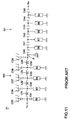
- FIG. 11 is an example of the circuit of a conventional antenna duplexer 81.
- Tx denotes a transmitting terminal
- Rx denotes a receiving terminal
- ANT denotes an antenna terminal
- 82-85 denote resonators of a transmitting circuit 100
- C31-C34 denote coupling capacitors to determine the magnitude of the attenuation in the blocking bandwidth
- C35-C39 denote capacitors
- L31-L34 denote coupling coils
- 86-90 denote resonators of a receiving circuit 101
- C40-C45 denote coupling capacitors.
- the transmission frequency bandwidth and the reception frequency bandwidth are wide, respective in the case of NTACS-CDMA, and the separation between the two is extremely small, and it is practically difficult to set the transmitting circuit 100 to be of high impedance in the reception frequency bandwidth and to set the receiving circuit 101 to be of high impedance in the transmission frequency bandwidth.
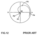
- FIG. 12 is a Smith chart of the antenna duplexer 81.
- P1, P2, P3 and P4 respectively indicates the impedance at the frequency of 832 MHz, 870 MHz, 887 MHz, and 925 MHz of the receiving circuit 101 viewed from a branch point A in FIG. 11.
- the frequency 832 MHz is the frequency at a low frequency side end part of the passing band of the receiving circuit 101 while the frequency 870 MHz is the frequency at a high frequency side end part of the passing band of the receiving circuit 101.
- the frequency 887 MHz is the frequency at a low frequency side end part of the passing band of the transmitting circuit 100 while the frequency 925 MHz is the frequency at a high frequency side end part of the passing band of the transmitting circuit 100.
- FIG. 12 is a Smith chart of the antenna duplexer 81.
- P1, P2, P3 and P4 respectively indicates the impedance at the frequency of 832 MHz, 870 MHz, 887 MHz, and 925 MHz of the receiving circuit 101
- the dielectric resonator is used in the transmitting circuit and the surface acoustic wave filter element is used in the receiving circuit.
- the transmitting circuit it is difficult to set the transmitting circuit to be of high impedance at the reception frequency bandwidth or to set the receiving circuit to be of high impedance at the transmission frequency bandwidth though the antenna duplexer can be miniaturized by using the surface acoustic wave filter element, and the insertion loss in the transmission and reception can not be improved. It is more rather superior in the characteristic aspect to compose the transmitting circuit and the receiving circuit of the dielectric resonator.
- an antenna duplexer 121 illustrated in FIG. 13 capable of switching two kinds of the passing bands of a transmitting circuit 130 and a receiving circuit 131 is proposed.
- FIG. 13 An antenna duplexer 121 illustrated in FIG. 13 capable of switching two kinds of the passing bands of a transmitting circuit 130 and a receiving circuit 131 is proposed.
- Tx denotes a transmitting terminal
- Rx denotes a receiving terminal
- ANT denotes an antenna terminal
- CONT denotes a voltage control terminal
- 122 and 123 denote resonators of the transmitting circuit 130
- 124-127 denote resonators of the receiving circuit 131
- L35 and L44 denote coupling coils
- C50 and C51 denote coupling capacitors to determine the magnitude of the attenuation of the blocking region
- C52 and C53 denote capacitors
- C54-C59 denote frequency variable bandwidth capacitors
- D11-D16 denote PIN diodes
- L36-L41 denote choke coils.
- R11, R12 and C60, C61 denote resistors and capacitors for supplying the control voltage, respectively, L42, L43 and C62 denote coils and a capacitor to constitute the phase shifter, respectively, C63-C65 denote coupling capacitors, and C66 and C67 denote a multi-pass capacitors to polarize the receiving circuit 131.
- the transmitting circuit 130 constitutes a variable bandwidth blocking circuit while the receiving circuit 131 constitutes the variable band passing circuit.
- the antenna duplexer 121 can apparently set the transmission frequency bandwidth and the reception frequency bandwidth to be small, and to increase the separation between the two.
- the antenna duplexer 121 is not suitable for miniaturization because it requires one of the PIN diodes D11-D16 and one of the choke coils L36-L41 for each of the resonators 122-127.
- degradation of the resonance system Q 0 (Q 0 is the Q at the center frequency) is not avoided because the PIN diodes D11-D16 and the capacitors C54-C59 are connected to a large number of resonators 122-127 in parallel.
- the insertion loss of the receiving circuit 131 to constitute the band passing circuit is dependent on the resonance system Q 0 , and electric degradation of the receiving circuit 131 is remarkable.
- the object of the present invention is to provide an antenna duplexer which is small in degradation of Q 0 of the resonance system, small in insertion loss and compact in size.
- a preferred embodiment of the present invention provides an antenna duplexer, comprising: a transmitting terminal; a receiving terminal; an antenna terminal; a transmitting circuit electrically connected between said transmitting terminal and said antenna terminal, said transmitting circuit comprising at least one first resonator and a first element electrically connected to said first resonator and electrically changing the capacitance by the control voltage; and a receiving circuit electrically connected between said receiving terminal and said antenna terminal, said receiving circuit comprising at least one second resonator, a second element electrically connected to said second resonator and electrically changing the capacitance by the control voltage, and a surface acoustic wave filter element.
- At least one selected from the group consisting of said first resonator and second resonator may be a dielectric resonator, and at least one selected from the group consisting of said first element electrically changing the capacitance and said second element electrically changing the capacitance may be a variable capacitance diode or a PIN diode, and the variable capacitance diode or the PIN diode may be electrically connected between an internal conductor of said dielectric resonator and a grounded external conductor of said dielectric resonator.
- said transmitting circuit may comprise a variable bandwidth blocking filter circuit and a first phase shifter
- said receiving circuit may comprise a variable trap circuit, a second phase shifter and a surface acoustic wave filter circuit.
- the first element electrically changing the capacitance of the transmitting circuit is controlled by the voltage, and the passing band of the transmitting circuit is switched, and the passing band of the receiving circuit is switched to the frequency of the transmitting circuit to apparently reduce the transmission frequency bandwidth of the transmitting circuit and the reception frequency bandwidth of the receiving circuit, and to increase the separation between the two, and to suppress the insertion loss of the transmitting circuit and the receiving circuit.
- the number of resonators of the receiving circuit and the number of diodes, etc. to be connected to the resonators can be greatly reduced by employing the surface acoustic wave filter element in the receiving circuit.
- the loss of the transmitting circuit can be suppressed by providing the trap circuit in the receiving circuit.
- the antenna duplexer which is less in degradation of Q 0 of the resonance system, low in the insertion loss, and compact in size.
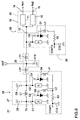
- FIG. 1 is a circuit constitution of an antenna duplexer 1.
- a transmitting circuit 25 is electrically connected between a transmitting terminal Tx and an antenna terminal ANT
- a receiving circuit 26 is electrically connected between receiving terminals Rx1, Rx2 and the antenna terminal ANT.
- the transmitting circuit 25 comprises a frequency variable bandwidth blocking filter circuit 27 and a first phase shifter 29.
- the bandwidth blocking filter circuit 27 comprises a resonator 2 to be electrically connected to the transmitting terminal Tx through a capacitor C1 for resonance, and a resonator 3 to be electrically connected to the first phase shifter 29 through a capacitor C2 for resonance.
- the capacitors C1, C2 for resonance are those to determine the magnitude of the attenuation of the blocking bandwidth.
- the series resonance circuit of the resonator 2 and the capacitor C1 for resonance is electrically connected to the series resonance circuit of the resonator 3 and the capacitor C2 for resonance through a coil L1 for coupling.
- capacitors C5, C6 are electrically connected in parallel to these two series resonance circuits.
- a series circuit of a variable bandwidth capacitor C3 and a PIN diode D1 is electrically connected in parallel to a resonator 2 in a condition where a cathode of the PIN diode D1 is grounded at an intermediate connection point of the resonator 2 to the capacitor C1 for resonance.
- a series circuit of a variable bandwidth capacitor C4 and a PIN diode D2 is electrically connected in parallel to a resonator 3 in a condition where a cathode of the PIN diode D2 is grounded at an intermediate connection point of the resonator 3 to the capacitor C2 for resonance.
- the variable bandwidth capacitors C3, C4 are used to change two attenuation polar frequencies of the attenuation characteristic of the frequency variable bandwidth blocking filter circuit 27.
- a voltage control terminal CONT1 is electrically connected to an intermediate connection point of an anode of the PIN diode D1 to the variable bandwidth capacitor C3 through a resistor R1 for supplying the control voltage, a capacitor C12, and a choke coil L2, and at the same time, electrically connected to an intermediate connection point of an anode of the PIN diode D2 to the variable bandwidth capacitor C4 through the resistor R1 for supplying the control voltage, the capacitor C12 and the choke coil L3.
- the first phase shifter 29 is a T-shaped circuit comprising a coil L10 which is electrically connected between the bandwidth blocking filter circuit 27 and the antenna terminal ANT, the capacitor C10 which is electrically connected between the ground and the antenna terminal ANT, and a coil L11 which is electrically connected between a frequency variable trap circuit 28 (to be mentioned below) of the receiving circuit 26, and the antenna terminal ANT.
- the receiving circuit 26 comprises the frequency variable trap circuit 28, the second phase shifter 29 and a surface acoustic wave filter circuit 30.
- the second phase shifter 29 is shared by a transmitting circuit 25, but it goes without saying that the transmitting circuit 25 and the receiving circuit 26 may be provided with each independent phase shifter.
- the surface acoustic wave filter circuit 30 is provided with surface acoustic wave filter elements 11, 12 which are respectively connected between the receiving terminals Rx1, Rx2 and the second phase shifter 29.
- the surface acoustic wave filter element 11 has the passing band of 832-846 MHz while the surface acoustic wave filter element 12 has the passing band of 860-870 MHz.
- the number of resonators and the number of diodes, etc., to be connected to the resonators can be greatly reduced by employing these surface acoustic wave filter elements 11,12.
- the surface acoustic wave filter circuit 30 comprises surface acoustic wave filter parts 10 provided with an input terminal 13, a ground terminal 16, and two output terminals 14,15 on two end face parts opposite to each other of a rectangular case 18 as illustrated in FIG. 2.
- the surface acoustic wave filter elements 11,12 are arranged inside the case 18 though they are not illustrated in FIG. 2, each input side of the filter elements 11,12 is connected to the common input terminal 13, the output side of the filter element 11 is connected to an output terminal 14, and the output side of the filter element 12 is connected to an output terminal 15. That means, the surface acoustic wave filter parts 10 are of one-input and two-output type, and suitable for miniaturization of the antenna duplexer. In a case of the first preferred embodiment, the surface acoustic wave filter parts 10 of 3.8 mm in length, 3.8 mm in width, and 1.5 mm in height is used.
- the frequency variable trap circuit 28 is provided with the resonator 4 which is electrically connected through the capacitor C7 for resonance at the intermediate connection point of the surface acoustic wave filter circuit 30 and the second phase shifter 29.
- the series circuit of the variable bandwidth capacitor C8 and the PIN diode D3 is electrically connected in parallel to the resonator 4 in a condition where a cathode of the PIN diode D3 is grounded at the intermediate connection point of the resonator 4 to the capacitor C7 for resonance.
- the voltage control terminal CONT2 is electrically connected to the intermediate connection point of an anode of the PIN diode D3 to the variable bandwidth capacitor C8 through the resistor R2 for supplying the control voltage, the capacitor C13, and a choke coil L4.
- a dielectric resonator is used in the resonators 2-4, as illustrated in FIG. 3.
- FIG. 3 illustrates the resonator 2 as an example.
- the dielectric resonators 2-4 comprise a cylindrical dielectric body 21 formed of the highly dielectric material such as TiO 2 ceramics, an external conductor 22 provided on the outer circumferential surface of the cylindrical dielectric body 21, and an internal conductor 23 provided on the inner circumferential surface of the cylindrical dielectric body 21.
- the external conductor 22 is electrically opened (disconnected) from the internal conductor 23 at one open end face 21a (hereinafter, referred to as the open side end face 21a) of the dielectric body 21, and electrically short-circuited (conducted) to the internal conductor 23 at the other open end face 21b (hereinafter, referred to as the short-circuited end face 21b).
- the series circuit of the variable bandwidth capacitor C3 and the PIN diode D1 is electrically connected at the open end face 21a in a condition where one end of the variable bandwidth capacitor C3 is connected to the internal conductor 23, and the cathode of the PIN diode D1 is connected to the external conductor 22.
- the series circuit of the variable bandwidth capacitor C4 and the PIN diode D2 is electrically connected at the open end face 21a in a condition where one end of the variable bandwidth capacitor C4 is connected to the internal conductor 23, and the cathode of the PIN diode D2 is connected to the external conductor 22.
- the series circuit of the variable bandwidth capacitor C8 and the PIN diode D3 is electrically connected at the open end face 21a in a condition where one end of the variable bandwidth capacitor C8 is connected to the internal conductor 23, and the cathode of the PIN diode D3 is connected to the external conductor 22.
- the external conductor is grounded at the short-circuited end face 21b.
- the transmission signal received by the transmitting terminal Tx from the transmitting circuit system is outputted from the antenna terminal ANT through the transmitting circuit 25, and the reception signal received by the antenna terminal ANT is outputted from the receiving terminals Rx1,Rx2 to the receiving circuit system through the receiving circuit 26.
- the trap frequency of the frequency variable bandwidth blocking filter circuit 27 of the transmitting circuit 25 is determined by each resonance frequency of the resonance system comprising the variable bandwidth capacitor C3, the capacitor C1 for resonance, and the resonator 2, and the resonance system comprising the variable bandwidth capacitor C4, the capacitor C2 for resonance, and the resonator 3.
- the PIN diodes D1, D2 are in the ON-condition.
- the variable bandwidth capacitors C3, C4 are respectively grounded through the PIN diodes D1, D2, two attenuation polar frequencies are reduced, and the passing band of the transmitting circuit 25 becomes 887-901 MHz.
- variable bandwidth capacitors C3, C4 are thus in the open condition, two attenuation polar frequencies are both increased, and the passing band of the transmitting circuit 25 becomes 915-925 MHz.
- FIG. 4 is a graph illustrating the results of the measurement of the passing characteristic S21 and the reflecting characteristic S11 of the transmitting circuit 25 when 887-901 MHz is selected as the passing band of the transmitting circuit 25.
- FIG. 5 is a graph illustrating the results of the measurement of the passing characteristic S21 and the reflecting characteristic S11 of the transmitting circuit 25 when 915-925 MHz is selected as the passing band of the transmitting circuit 25.
- the transmitting circuit 25 can have two different passing band characteristics by grounding or opening the variable bandwidth capacitors C3,C4 by controlling the voltage.
- the receiving circuit 26 outputs only the signal passing the surface acoustic wave filter element 11 when the receiving terminal Rx1 is in the ON-condition and the receiving terminal Rx2 is in the OFF-condition.
- the passing band of the receiving circuit 26 becomes 832-846 MHz.
- the receiving circuit outputs only the signal passing the surface acoustic wave filter element 12 when the receiving terminal Rx1 is in the OFF-condition and the receiving terminal Rx2 is in the ON-condition.
- the passing band of the receiving circuit 26 becomes 860-870 MHz.
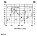
- FIG. 6 is a graph illustrating the results of the measurement of the passing characteristic S32 and the reflecting characteristic S33 of the receiving circuit 26 when 832-846 MHz is selected as the passing band of the receiving circuit 26.
- FIG. 7 is a graph illustrating the results of the measurement of the passing characteristic S32 and the reflecting characteristic S33 of the receiving circuit 26 when 860-870 MHz is selected as the passing band of the receiving circuit 26.
- the receiving circuit 26 can have two different passing band characteristics by setting either of the receiving terminal Rx1 or Rx2 in the ON-condition.
- the transmitting circuit 25 when the positive control voltage is applied to the voltage control terminal CONT1 to set the transmission frequency bandwidth of the transmitting circuit 25 to be 887-901 MHz (refer to FIG. 4), the receiving terminal Rx1 is set in the ON-condition and the receiving terminal Rx2 is in the OFF-condition to set the reception frequency bandwidth of the receiving circuit 26 to be 832-846 MHz. (Refer to FIG. 6.)
- the separation between the transmission frequency bandwidth of the transmitting circuit 25 and the reception frequency bandwidth of the receiving circuit 26 can be increased as high as 55 MHz, and the insertion loss can also be suppressed.
- the transmitting circuit 25 is easily set so that the impedance is high at the reception frequency bandwidth 832-846 MHz (refer to FIG. 4), and the insertion loss of the receiving circuit 26 is not remarkably degraded.
- the receiving circuit 26 is easily set so that the impedance is high at the transmission frequency bandwidth 887-901 MHz (refer to FIG. 6), and the insertion loss of the transmitting circuit 25 is not remarkably degraded.
- the transmitting circuit 25 when the negative control voltage is applied to the voltage control terminal CONT1 to set the transmission frequency bandwidth of the transmitting circuit 25 to be 915-925 MHz (refer to FIG. 5), the receiving terminal Rx1 is set in the OFF-condition and the receiving terminal Rx2 is in the ON-condition to set the reception frequency bandwidth of the receiving circuit 26 to be 860-870 MHz. (Refer to FIG. 7.)
- the separation between the transmission frequency bandwidth of the transmitting circuit 25 and the reception frequency bandwidth of the receiving circuit 26 can be increased as high as 55 MHz, and the insertion loss can also be suppressed.
- the transmitting circuit 25 is easily set so that the impedance is high at the reception frequency bandwidth 860-870 MHz (refer to FIG. 5), and the insertion loss of the receiving circuit 26 is not remarkably degraded.
- the receiving circuit 26 is easily set so that the impedance is high at the transmission frequency bandwidth 915-925 MHz (refer to FIG. 7), and the insertion loss of the transmitting circuit 25 is not remarkably degraded.
- the trap frequency of the frequency variable trap circuit 28 of the receiving circuit 26 is also determined by the resonance frequency of the resonance system comprising the variable bandwidth capacitor C8, the capacitor C7 for resonance and the resonator 4.
- the resonance frequency of the resonance system comprising the variable bandwidth capacitor C8, the capacitor C7 for resonance and the resonator 4.
- the voltage is controlled so that the trap frequency becomes low when 887-901 MHz is selected as the transmitting band to meet the switching of two passing bands of 887-901 MHz and 915-925MHz of the transmitting circuit 25, while the trap frequency becomes high when 915-925 MHz is selected as the passing band.
- the phase synthesis with the transmitting circuit 25 can be ideally performed.
- the receiving circuit 26 can be easily set to be of high impedance at the transmission frequency bandwidth of 887-901 MHz and 915-925 MHz by providing the frequency variable trap circuit 28 in the receiving circuit 26.
- the matching loss of the transmitting circuit 25 with the receiving circuit 26 is suppressed, and the insertion loss of the transmitting circuit 25 is not greatly degraded.
- FIG. 8 is a Smith chart of the antenna duplexer 1.
- P1, P2, P3 and P4 indicates the impedance at the frequency 832MHz, 870 MHz, 887 MHz, and 925 MHz of the receiving circuit 26 viewed from the branch point B in FIG. 1.
- the frequency 832 MHz is the low frequency side end part of the passing band of the receiving circuit 26, while the frequency 870 MHz is the high frequency side end part of the passing band of the receiving circuit 26.
- the frequency 887 MHz is the low frequency side end part of the passing band of the transmitting circuit 25 while the frequency 925 MHz is the high frequency side end part of the passing band of the transmitting circuit 25.
- the antenna duplexer 1 is high in the impedance of the receiving circuit 26 at P3 of the frequency 887 MHz, and it is understood that the insertion loss of the antenna duplexer 1 during the transmission is small.
- an antenna duplexer 41 of the second preferred embodiment employs variable capacitance diodes D5-D7 in place of PIN diodes D1-D3 in the antenna duplexer 1 of the embodiment illustrated in FIG. 1 through FIG. 3.
- the trap frequency of a frequency variable bandwidth blocking filter circuit 27 of the transmitting circuit 25 is determined by the capacitance of a variable capacitance diode D5, the resonance frequency of the resonance system comprising the variable bandwidth capacitor C3, capacitor C1 for resonance, and the resonator 2, the capacitance of a variable capacitance diode D6, and the resonance frequency of the resonance system comprising the variable bandwidth capacitor C4, the capacitor C2 for resonance and the resonator 3.
- the capacitance of the variable capacitance diodes D5,D6 is changed by changing the voltage to be applied to the voltage control terminal CONT 1. As a result, the attenuation pole of the frequency variable bandwidth blocking filter circuit 27 is moved, and the trap frequency is changed.
- the transmitting circuit 25 can have two different passing bands by changing the capacitance of the variable capacitance diodes D5,D6 by controlling the voltage.
- the trap frequency of the frequency variable trap circuit 28 of the receiving circuit 26 is also determined by the capacitance of a variable capacitance diode D7, and the resonance frequency of the resonance system comprising the variable bandwidth capacitor C8, the resonance capacitor C7, and the resonator 4.
- the capacitance of the variable capacitance diode D7 is changed by changing the voltage to be applied to the voltage control terminal CONT2. As a result, the trap frequency of the frequency variable trap circuit 28 is changed.
- variable bandwidth capacitor C3 of the series circuit comprising the variable bandwidth capacitor C3 and the variable capacitance diode D5
- the internal conductor 23 at the open end face 21a, and is electrically connected in a condition where the cathode of the variable capacitance diode D5 is connected to the external conductor 22.
- one end of the variable bandwidth capacitor C4 of the series circuit comprising the variable bandwidth capacitor C4 and the variable capacitance diode D6 is connected to the internal conductor 23 at the open end face 21a, and is electrically connected in a condition where the cathode of the variable capacitance diode D6 is connected to the external conductor 22.
- one end of the variable bandwidth capacitor C8 of the series circuit comprising the variable bandwidth capacitor C8 and the variable capacitance diode D7 is connected to the internal conductor 23 at the open end face 21a, and is electrically connected in a condition where the cathode of the variable capacitance diode D7 is connected to the external conductor 22.
- the antenna duplexer 41 of the second preferred embodiment takes similar effect to that of the antenna duplexer 1 of the first embodiment.
- the antenna duplexer of the present invention is not limited to the above-mentioned embodiments, but can be changed diversely in the range of the summary.
- the resonator may be a strip line resonator, etc., in addition to the dielectric resonator.
- the number of the resonators is arbitrary.
Abstract
Description
- The present invention relates to an antenna duplexer, more specifically, the antenna duplexer to be used for a microwave band communication equipment or the like.
- For example, there is a portable telephone system having a plurality of passing bands of a transmitting circuit and a receiving circuit such as NTACS-CDMA. In the case of NTACS-CDMA, the frequency is allotted to 887-901 MHz and 915-925 MHz for the transmission side, and 832-846 MHz and 860-870 MHz for the reception side, having two kinds of passing bands, respectively. Thus, the transmission frequency bandwidth to be required for the transmitting circuit of the antenna duplexer to be used for NTACS-CDMA is 887-925 MHz while the reception frequency bandwidth to be required for the receiving circuit is 832-870 MHz, and both the transmitting circuit and the receiving circuit are required to have the wide passing hand of 38 MHz. On the other hand, the separation to be secured to separate the transmission frequency bandwidth from the reception frequency bandwidth is 17 MHz, and the separation between the two becomes extremely small.
- The antenna duplexer synthesizes the phase of the transmitting circuit with the phase of the receiving circuit. In the case of NTACS-CDMA, the transmitting circuit is set to be of high impedance (open) at the reception frequency bandwidth of 832-870 MHz, and the receiving circuit is set to be of high impedance (open) at the transmission frequency bandwidth of 887-925 MHz to ideally synthesize the phase of the transmitting circuit with the phase of the receiving circuit.
- FIG. 11 is an example of the circuit of a
conventional antenna duplexer 81. In FIG. 11, Tx denotes a transmitting terminal, Rx denotes a receiving terminal, ANT denotes an antenna terminal, 82-85 denote resonators of a transmittingcircuit 100, C31-C34 denote coupling capacitors to determine the magnitude of the attenuation in the blocking bandwidth, C35-C39 denote capacitors, L31-L34 denote coupling coils, 86-90 denote resonators of areceiving circuit 101, and C40-C45 denote coupling capacitors. - In the
conventional antenna duplexer 81, however, the transmission frequency bandwidth and the reception frequency bandwidth are wide, respective in the case of NTACS-CDMA, and the separation between the two is extremely small, and it is practically difficult to set the transmittingcircuit 100 to be of high impedance in the reception frequency bandwidth and to set thereceiving circuit 101 to be of high impedance in the transmission frequency bandwidth. - FIG. 12 is a Smith chart of the
antenna duplexer 81. In FIG. 12, P1, P2, P3 and P4 respectively indicates the impedance at the frequency of 832 MHz, 870 MHz, 887 MHz, and 925 MHz of thereceiving circuit 101 viewed from a branch point A in FIG. 11. The frequency 832 MHz is the frequency at a low frequency side end part of the passing band of thereceiving circuit 101 while the frequency 870 MHz is the frequency at a high frequency side end part of the passing band of thereceiving circuit 101. The frequency 887 MHz is the frequency at a low frequency side end part of the passing band of thetransmitting circuit 100 while the frequency 925 MHz is the frequency at a high frequency side end part of the passing band of the transmittingcircuit 100. FIG. 12 shows that the impedance of thereceiving circuit 101 at P3 of the frequency of 887 MHz is low, and the insertion loss of theantenna duplexer 81 in transmission is increased. To cope with the problem, Q0 is increased by increasing the size of the dielectric resonator of the transmitting circuit and the receiving circuit in order to obtain the steep attenuation curve, but there raises another problem that the size of theantenna duplexer 81 is increased. - As a method for miniaturizing the antenna duplexer, a proposal is made that the dielectric resonator is used in the transmitting circuit and the surface acoustic wave filter element is used in the receiving circuit. (For example, refer to Japanese Unexamined Patent Publication No. 5-95204.) However, it is difficult to set the transmitting circuit to be of high impedance at the reception frequency bandwidth or to set the receiving circuit to be of high impedance at the transmission frequency bandwidth though the antenna duplexer can be miniaturized by using the surface acoustic wave filter element, and the insertion loss in the transmission and reception can not be improved. It is more rather superior in the characteristic aspect to compose the transmitting circuit and the receiving circuit of the dielectric resonator.
- Also, as the method to set the transmitting circuit to be of high impedance at the reception frequency bandwidth and to set the receiving circuit to be of high impedance at the transmission frequency bandwidth, an
antenna duplexer 121 illustrated in FIG. 13 capable of switching two kinds of the passing bands of a transmittingcircuit 130 and areceiving circuit 131 is proposed. In FIG. 13, Tx denotes a transmitting terminal, Rx denotes a receiving terminal, ANT denotes an antenna terminal, CONT denotes a voltage control terminal, 122 and 123 denote resonators of the transmittingcircuit 130, 124-127 denote resonators of thereceiving circuit 131, L35 and L44 denote coupling coils, C50 and C51 denote coupling capacitors to determine the magnitude of the attenuation of the blocking region, C52 and C53 denote capacitors, C54-C59 denote frequency variable bandwidth capacitors, D11-D16 denote PIN diodes, L36-L41 denote choke coils. R11, R12 and C60, C61 denote resistors and capacitors for supplying the control voltage, respectively, L42, L43 and C62 denote coils and a capacitor to constitute the phase shifter, respectively, C63-C65 denote coupling capacitors, and C66 and C67 denote a multi-pass capacitors to polarize thereceiving circuit 131. The transmittingcircuit 130 constitutes a variable bandwidth blocking circuit while thereceiving circuit 131 constitutes the variable band passing circuit. - The
antenna duplexer 121 can apparently set the transmission frequency bandwidth and the reception frequency bandwidth to be small, and to increase the separation between the two. However, there is a problem that theantenna duplexer 121 is not suitable for miniaturization because it requires one of the PIN diodes D11-D16 and one of the choke coils L36-L41 for each of the resonators 122-127. In addition, degradation of the resonance system Q0 (Q0 is the Q at the center frequency) is not avoided because the PIN diodes D11-D16 and the capacitors C54-C59 are connected to a large number of resonators 122-127 in parallel. In particular, the insertion loss of thereceiving circuit 131 to constitute the band passing circuit is dependent on the resonance system Q0, and electric degradation of thereceiving circuit 131 is remarkable. - The object of the present invention is to provide an antenna duplexer which is small in degradation of Q0 of the resonance system, small in insertion loss and compact in size.
- A preferred embodiment of the present invention provides an antenna duplexer, comprising: a transmitting terminal; a receiving terminal; an antenna terminal; a transmitting circuit electrically connected between said transmitting terminal and said antenna terminal, said transmitting circuit comprising at least one first resonator and a first element electrically connected to said first resonator and electrically changing the capacitance by the control voltage; and a receiving circuit electrically connected between said receiving terminal and said antenna terminal, said receiving circuit comprising at least one second resonator, a second element electrically connected to said second resonator and electrically changing the capacitance by the control voltage, and a surface acoustic wave filter element.
- In the above described antenna duplexer, at least one selected from the group consisting of said first resonator and second resonator may be a dielectric resonator, and at least one selected from the group consisting of said first element electrically changing the capacitance and said second element electrically changing the capacitance may be a variable capacitance diode or a PIN diode, and the variable capacitance diode or the PIN diode may be electrically connected between an internal conductor of said dielectric resonator and a grounded external conductor of said dielectric resonator.
- In the above described antenna duplexer, said transmitting circuit may comprise a variable bandwidth blocking filter circuit and a first phase shifter, and said receiving circuit may comprise a variable trap circuit, a second phase shifter and a surface acoustic wave filter circuit.
- According to the present invention, the first element electrically changing the capacitance of the transmitting circuit is controlled by the voltage, and the passing band of the transmitting circuit is switched, and the passing band of the receiving circuit is switched to the frequency of the transmitting circuit to apparently reduce the transmission frequency bandwidth of the transmitting circuit and the reception frequency bandwidth of the receiving circuit, and to increase the separation between the two, and to suppress the insertion loss of the transmitting circuit and the receiving circuit. The number of resonators of the receiving circuit and the number of diodes, etc. to be connected to the resonators can be greatly reduced by employing the surface acoustic wave filter element in the receiving circuit. The loss of the transmitting circuit can be suppressed by providing the trap circuit in the receiving circuit. As a result, the antenna duplexer which is less in degradation of Q0 of the resonance system, low in the insertion loss, and compact in size.
- Other features and advantages of the present invention will become apparent from the following description of preferred embodiments of the invention which refers to the accompanying drawings, wherein like reference numerals indicate like elements to avoid duplicative description.
-
- FIG. 1 is an electric circuit illustrating the constitution of the first preferred embodiment of the antenna duplexer of the present invention.
- FIG. 2 is a perspective view illustrating the appearance of a surface acoustic wave filter to be used for the antenna duplexer illustrated in FIG. 1.
- FIG. 3 is a sectional view illustrating one example of a dielectric resonator to be used for the antenna duplexer illustrated in FIG. 1.
- FIG. 4 is a graph illustrating the transmission and reflection characteristics of the transmitting circuit illustrated in FIG. 1 when 887-901 MHz is selected as the passing band.
- FIG. 5 is a graph illustrating the transmission and reflection characteristics of the transmitting circuit illustrated in FIG. 1 when 915-925 MHz is selected as the passing band.
- FIG. 6 is a graph illustrating the transmission and reflection characteristics of the receiving circuit illustrated in FIG. 1 when 832-846 MHz is selected as the passing band.
- FIG. 7 is a graph illustrating the transmission and reflection characteristics of the receiving circuit illustrated in FIG. 1 when 860-870 MHz is selected as the passing band.
- FIG. 8 is a Smith chart of the antenna duplexer illustrated in FIG. 1.
- FIG. 9 is an electric circuit diagram illustrating the constitution of the second preferred embodiment of the antenna duplexer of the present invention.
- FIG. 10 is a section illustrating one example of the dielectric resonator to be used for the antenna duplexer illustrated in FIG. 9.
- FIG. 11 is an electric circuit diagram illustrating the constitution of a conventional antenna duplexer.
- FIG. 12 is a Smith chart of the antenna duplexer illustrated in FIG. 11.
- FIG. 13 is an electric circuit diagram illustrating the constitution of another conventional antenna duplexer.
-
- FIG. 1 is a circuit constitution of an
antenna duplexer 1. In theantenna duplexer 1, a transmittingcircuit 25 is electrically connected between a transmitting terminal Tx and an antenna terminal ANT, and areceiving circuit 26 is electrically connected between receiving terminals Rx1, Rx2 and the antenna terminal ANT. - The
transmitting circuit 25 comprises a frequency variable bandwidthblocking filter circuit 27 and afirst phase shifter 29. The bandwidthblocking filter circuit 27 comprises aresonator 2 to be electrically connected to the transmitting terminal Tx through a capacitor C1 for resonance, and aresonator 3 to be electrically connected to thefirst phase shifter 29 through a capacitor C2 for resonance. The capacitors C1, C2 for resonance are those to determine the magnitude of the attenuation of the blocking bandwidth. The series resonance circuit of theresonator 2 and the capacitor C1 for resonance is electrically connected to the series resonance circuit of theresonator 3 and the capacitor C2 for resonance through a coil L1 for coupling. In addition, capacitors C5, C6 are electrically connected in parallel to these two series resonance circuits. - A series circuit of a variable bandwidth capacitor C3 and a PIN diode D1 is electrically connected in parallel to a
resonator 2 in a condition where a cathode of the PIN diode D1 is grounded at an intermediate connection point of theresonator 2 to the capacitor C1 for resonance. Similarly, a series circuit of a variable bandwidth capacitor C4 and a PIN diode D2 is electrically connected in parallel to aresonator 3 in a condition where a cathode of the PIN diode D2 is grounded at an intermediate connection point of theresonator 3 to the capacitor C2 for resonance. The variable bandwidth capacitors C3, C4 are used to change two attenuation polar frequencies of the attenuation characteristic of the frequency variable bandwidth blockingfilter circuit 27. - A voltage control terminal CONT1 is electrically connected to an intermediate connection point of an anode of the PIN diode D1 to the variable bandwidth capacitor C3 through a resistor R1 for supplying the control voltage, a capacitor C12, and a choke coil L2, and at the same time, electrically connected to an intermediate connection point of an anode of the PIN diode D2 to the variable bandwidth capacitor C4 through the resistor R1 for supplying the control voltage, the capacitor C12 and the choke coil L3.
- The
first phase shifter 29 is a T-shaped circuit comprising a coil L10 which is electrically connected between the bandwidth blockingfilter circuit 27 and the antenna terminal ANT, the capacitor C10 which is electrically connected between the ground and the antenna terminal ANT, and a coil L11 which is electrically connected between a frequency variable trap circuit 28 (to be mentioned below) of the receivingcircuit 26, and the antenna terminal ANT. - The receiving
circuit 26 comprises the frequencyvariable trap circuit 28, thesecond phase shifter 29 and a surface acousticwave filter circuit 30. In a case of the receivingcircuit 26 of the first embodiment, thesecond phase shifter 29 is shared by a transmittingcircuit 25, but it goes without saying that the transmittingcircuit 25 and the receivingcircuit 26 may be provided with each independent phase shifter. - The surface acoustic
wave filter circuit 30 is provided with surface acousticwave filter elements second phase shifter 29. The surface acousticwave filter element 11 has the passing band of 832-846 MHz while the surface acousticwave filter element 12 has the passing band of 860-870 MHz. The number of resonators and the number of diodes, etc., to be connected to the resonators can be greatly reduced by employing these surface acousticwave filter elements - The surface acoustic
wave filter circuit 30 comprises surface acousticwave filter parts 10 provided with aninput terminal 13, aground terminal 16, and twooutput terminals rectangular case 18 as illustrated in FIG. 2. The surface acousticwave filter elements case 18 though they are not illustrated in FIG. 2, each input side of thefilter elements common input terminal 13, the output side of thefilter element 11 is connected to anoutput terminal 14, and the output side of thefilter element 12 is connected to anoutput terminal 15. That means, the surface acousticwave filter parts 10 are of one-input and two-output type, and suitable for miniaturization of the antenna duplexer. In a case of the first preferred embodiment, the surface acousticwave filter parts 10 of 3.8 mm in length, 3.8 mm in width, and 1.5 mm in height is used. - The frequency
variable trap circuit 28 is provided with theresonator 4 which is electrically connected through the capacitor C7 for resonance at the intermediate connection point of the surface acousticwave filter circuit 30 and thesecond phase shifter 29. The series circuit of the variable bandwidth capacitor C8 and the PIN diode D3 is electrically connected in parallel to theresonator 4 in a condition where a cathode of the PIN diode D3 is grounded at the intermediate connection point of theresonator 4 to the capacitor C7 for resonance. The voltage control terminal CONT2 is electrically connected to the intermediate connection point of an anode of the PIN diode D3 to the variable bandwidth capacitor C8 through the resistor R2 for supplying the control voltage, the capacitor C13, and a choke coil L4. - A dielectric resonator is used in the resonators 2-4, as illustrated in FIG. 3. FIG. 3 illustrates the
resonator 2 as an example. The dielectric resonators 2-4 comprise a cylindricaldielectric body 21 formed of the highly dielectric material such as TiO2 ceramics, anexternal conductor 22 provided on the outer circumferential surface of the cylindricaldielectric body 21, and aninternal conductor 23 provided on the inner circumferential surface of the cylindricaldielectric body 21. Theexternal conductor 22 is electrically opened (disconnected) from theinternal conductor 23 at oneopen end face 21a (hereinafter, referred to as the openside end face 21a) of thedielectric body 21, and electrically short-circuited (conducted) to theinternal conductor 23 at the otheropen end face 21b (hereinafter, referred to as the short-circuitedend face 21b). In thedielectric resonator 2, the series circuit of the variable bandwidth capacitor C3 and the PIN diode D1 is electrically connected at theopen end face 21a in a condition where one end of the variable bandwidth capacitor C3 is connected to theinternal conductor 23, and the cathode of the PIN diode D1 is connected to theexternal conductor 22. - Similarly, in the
dielectric resonator 3, the series circuit of the variable bandwidth capacitor C4 and the PIN diode D2 is electrically connected at theopen end face 21a in a condition where one end of the variable bandwidth capacitor C4 is connected to theinternal conductor 23, and the cathode of the PIN diode D2 is connected to theexternal conductor 22. In thedielectric resonator 4, the series circuit of the variable bandwidth capacitor C8 and the PIN diode D3 is electrically connected at theopen end face 21a in a condition where one end of the variable bandwidth capacitor C8 is connected to theinternal conductor 23, and the cathode of the PIN diode D3 is connected to theexternal conductor 22. In thedielectric resonators end face 21b. - The operation and advantages of the
antenna duplexer 1 of the above-mentioned constitution are explained hereinafter. In theantenna duplexer 1, the transmission signal received by the transmitting terminal Tx from the transmitting circuit system is outputted from the antenna terminal ANT through the transmittingcircuit 25, and the reception signal received by the antenna terminal ANT is outputted from the receiving terminals Rx1,Rx2 to the receiving circuit system through the receivingcircuit 26. - The trap frequency of the frequency variable bandwidth blocking
filter circuit 27 of the transmittingcircuit 25 is determined by each resonance frequency of the resonance system comprising the variable bandwidth capacitor C3, the capacitor C1 for resonance, and theresonator 2, and the resonance system comprising the variable bandwidth capacitor C4, the capacitor C2 for resonance, and theresonator 3. When the positive voltage as the control voltage is applied to the voltage control terminal CONT1, the PIN diodes D1, D2 are in the ON-condition. Thus, the variable bandwidth capacitors C3, C4 are respectively grounded through the PIN diodes D1, D2, two attenuation polar frequencies are reduced, and the passing band of the transmittingcircuit 25 becomes 887-901 MHz. - On the contrary, when the negative voltage is applied as the control voltage, the PIN diodes D1,D2 are in the OFF-condition. The variable bandwidth capacitors C3, C4 are thus in the open condition, two attenuation polar frequencies are both increased, and the passing band of the transmitting
circuit 25 becomes 915-925 MHz. - FIG. 4 is a graph illustrating the results of the measurement of the passing characteristic S21 and the reflecting characteristic S11 of the transmitting
circuit 25 when 887-901 MHz is selected as the passing band of the transmittingcircuit 25. FIG. 5 is a graph illustrating the results of the measurement of the passing characteristic S21 and the reflecting characteristic S11 of the transmittingcircuit 25 when 915-925 MHz is selected as the passing band of the transmittingcircuit 25. Thus, the transmittingcircuit 25 can have two different passing band characteristics by grounding or opening the variable bandwidth capacitors C3,C4 by controlling the voltage. - On the other hand, the receiving
circuit 26 outputs only the signal passing the surface acousticwave filter element 11 when the receiving terminal Rx1 is in the ON-condition and the receiving terminal Rx2 is in the OFF-condition. Thus, the passing band of the receivingcircuit 26 becomes 832-846 MHz. On the contrary, the receiving circuit outputs only the signal passing the surface acousticwave filter element 12 when the receiving terminal Rx1 is in the OFF-condition and the receiving terminal Rx2 is in the ON-condition. Thus, the passing band of the receivingcircuit 26 becomes 860-870 MHz. - FIG. 6 is a graph illustrating the results of the measurement of the passing characteristic S32 and the reflecting characteristic S33 of the receiving
circuit 26 when 832-846 MHz is selected as the passing band of the receivingcircuit 26. FIG. 7 is a graph illustrating the results of the measurement of the passing characteristic S32 and the reflecting characteristic S33 of the receivingcircuit 26 when 860-870 MHz is selected as the passing band of the receivingcircuit 26. Thus, the receivingcircuit 26 can have two different passing band characteristics by setting either of the receiving terminal Rx1 or Rx2 in the ON-condition. - In the transmitting
circuit 25, when the positive control voltage is applied to the voltage control terminal CONT1 to set the transmission frequency bandwidth of the transmittingcircuit 25 to be 887-901 MHz (refer to FIG. 4), the receiving terminal Rx1 is set in the ON-condition and the receiving terminal Rx2 is in the OFF-condition to set the reception frequency bandwidth of the receivingcircuit 26 to be 832-846 MHz. (Refer to FIG. 6.) The separation between the transmission frequency bandwidth of the transmittingcircuit 25 and the reception frequency bandwidth of the receivingcircuit 26 can be increased as high as 55 MHz, and the insertion loss can also be suppressed. - In addition, the transmitting
circuit 25 is easily set so that the impedance is high at the reception frequency bandwidth 832-846 MHz (refer to FIG. 4), and the insertion loss of the receivingcircuit 26 is not remarkably degraded. Similarly, the receivingcircuit 26 is easily set so that the impedance is high at the transmission frequency bandwidth 887-901 MHz (refer to FIG. 6), and the insertion loss of the transmittingcircuit 25 is not remarkably degraded. - In the transmitting
circuit 25, when the negative control voltage is applied to the voltage control terminal CONT1 to set the transmission frequency bandwidth of the transmittingcircuit 25 to be 915-925 MHz (refer to FIG. 5), the receiving terminal Rx1 is set in the OFF-condition and the receiving terminal Rx2 is in the ON-condition to set the reception frequency bandwidth of the receivingcircuit 26 to be 860-870 MHz. (Refer to FIG. 7.) The separation between the transmission frequency bandwidth of the transmittingcircuit 25 and the reception frequency bandwidth of the receivingcircuit 26 can be increased as high as 55 MHz, and the insertion loss can also be suppressed. - In addition, the transmitting
circuit 25 is easily set so that the impedance is high at the reception frequency bandwidth 860-870 MHz (refer to FIG. 5), and the insertion loss of the receivingcircuit 26 is not remarkably degraded. Similarly, the receivingcircuit 26 is easily set so that the impedance is high at the transmission frequency bandwidth 915-925 MHz (refer to FIG. 7), and the insertion loss of the transmittingcircuit 25 is not remarkably degraded. - The trap frequency of the frequency
variable trap circuit 28 of the receivingcircuit 26 is also determined by the resonance frequency of the resonance system comprising the variable bandwidth capacitor C8, the capacitor C7 for resonance and theresonator 4. When the positive voltage is applied to the voltage control terminal CONT2 as the control voltage, the PIN diode D3 is in the ON-condition. Thus, the variable bandwidth capacitor C8 is grounded through the PIN diode D3, and the trap frequency becomes low. On the contrary, when the negative voltage is applied as the control voltage, the PIN diode D3 is in the OFF-condition. Thus, the variable bandwidth capacitor C8 is in the open condition, and the trap frequency becomes high. - In the frequency
variable trap circuit 28, the voltage is controlled so that the trap frequency becomes low when 887-901 MHz is selected as the transmitting band to meet the switching of two passing bands of 887-901 MHz and 915-925MHz of the transmittingcircuit 25, while the trap frequency becomes high when 915-925 MHz is selected as the passing band. The phase synthesis with the transmittingcircuit 25 can be ideally performed. - The receiving
circuit 26 can be easily set to be of high impedance at the transmission frequency bandwidth of 887-901 MHz and 915-925 MHz by providing the frequencyvariable trap circuit 28 in the receivingcircuit 26. Thus, the matching loss of the transmittingcircuit 25 with the receivingcircuit 26 is suppressed, and the insertion loss of the transmittingcircuit 25 is not greatly degraded. - FIG. 8 is a Smith chart of the
antenna duplexer 1. In FIG. 8, P1, P2, P3 and P4 indicates the impedance at the frequency 832MHz, 870 MHz, 887 MHz, and 925 MHz of the receivingcircuit 26 viewed from the branch point B in FIG. 1. The frequency 832 MHz is the low frequency side end part of the passing band of the receivingcircuit 26, while the frequency 870 MHz is the high frequency side end part of the passing band of the receivingcircuit 26. The frequency 887 MHz is the low frequency side end part of the passing band of the transmittingcircuit 25 while the frequency 925 MHz is the high frequency side end part of the passing band of the transmittingcircuit 25. In comparing FIG. 8 with the Smith chart of theconventional antenna duplexer 81 illustrated in FIG. 12, theantenna duplexer 1 is high in the impedance of the receivingcircuit 26 at P3 of the frequency 887 MHz, and it is understood that the insertion loss of theantenna duplexer 1 during the transmission is small. - As illustrated in FIG. 9 and FIG. 10, an
antenna duplexer 41 of the second preferred embodiment employs variable capacitance diodes D5-D7 in place of PIN diodes D1-D3 in theantenna duplexer 1 of the embodiment illustrated in FIG. 1 through FIG. 3. - The trap frequency of a frequency variable bandwidth blocking
filter circuit 27 of the transmittingcircuit 25 is determined by the capacitance of a variable capacitance diode D5, the resonance frequency of the resonance system comprising the variable bandwidth capacitor C3, capacitor C1 for resonance, and theresonator 2, the capacitance of a variable capacitance diode D6, and the resonance frequency of the resonance system comprising the variable bandwidth capacitor C4, the capacitor C2 for resonance and theresonator 3. The capacitance of the variable capacitance diodes D5,D6 is changed by changing the voltage to be applied to the voltagecontrol terminal CONT 1. As a result, the attenuation pole of the frequency variable bandwidth blockingfilter circuit 27 is moved, and the trap frequency is changed. Thus, the transmittingcircuit 25 can have two different passing bands by changing the capacitance of the variable capacitance diodes D5,D6 by controlling the voltage. - The trap frequency of the frequency
variable trap circuit 28 of the receivingcircuit 26 is also determined by the capacitance of a variable capacitance diode D7, and the resonance frequency of the resonance system comprising the variable bandwidth capacitor C8, the resonance capacitor C7, and theresonator 4. The capacitance of the variable capacitance diode D7 is changed by changing the voltage to be applied to the voltage control terminal CONT2. As a result, the trap frequency of the frequencyvariable trap circuit 28 is changed. - In addition, in the
dielectric resonator 2 as illustrated in FIG. 10, one end of the variable bandwidth capacitor C3 of the series circuit comprising the variable bandwidth capacitor C3 and the variable capacitance diode D5, is connected to theinternal conductor 23 at theopen end face 21a, and is electrically connected in a condition where the cathode of the variable capacitance diode D5 is connected to theexternal conductor 22. Similarly, in thedielectric resonator 3, one end of the variable bandwidth capacitor C4 of the series circuit comprising the variable bandwidth capacitor C4 and the variable capacitance diode D6, is connected to theinternal conductor 23 at theopen end face 21a, and is electrically connected in a condition where the cathode of the variable capacitance diode D6 is connected to theexternal conductor 22. In thedielectric resonator 4, one end of the variable bandwidth capacitor C8 of the series circuit comprising the variable bandwidth capacitor C8 and the variable capacitance diode D7, is connected to theinternal conductor 23 at theopen end face 21a, and is electrically connected in a condition where the cathode of the variable capacitance diode D7 is connected to theexternal conductor 22. - The
antenna duplexer 41 of the second preferred embodiment takes similar effect to that of theantenna duplexer 1 of the first embodiment. - The antenna duplexer of the present invention is not limited to the above-mentioned embodiments, but can be changed diversely in the range of the summary. For example, the resonator may be a strip line resonator, etc., in addition to the dielectric resonator. The number of the resonators is arbitrary.
- While the invention has been particularly shown and described with reference to preferred embodiments thereof, it will be understood by those skilled man in the art that the forgoing and other changes in form and details may be made therein without departing from the spirit of the invention.
Claims (4)
- An antenna duplexer (1; 41), comprising:a transmitting terminal (Tx);a receiving terminal (Rx1, Rx2);an antenna terminal (ANT);a transmitting circuit (25) electrically connected between said transmitting terminal (Tx) and said antenna terminal (ANT), said transmitting circuit (25) comprising at least one first resonator (2, 3) and a first element electrically connected to said first resonator and electrically changing the capacitance by the control voltage (CONT1); anda receiving circuit (26) electrically connected between said receiving terminal (Rx1, Rx2) and said antenna terminal (ANT), said receiving circuit (26) comprising at least one second resonator (4), a second element electrically connected to said second resonator (4) and electrically changing the capacitance by the control voltage (CONT2), and a surface acoustic wave filter element (11, 12).
- The antenna duplexer (41) according to Claim 1, wherein at least one selected from the group consisting of said first resonator (2, 3) and second resonator (4) is a dielectric resonator, and at least one selected from the group consisting of said first element electrically changing the capacitance and said second element electrically changing the capacitance is a variable capacitance diode (D5, D6, D7), and the variable capacitance diode (D5, D6, D7) is electrically connected between an internal conductor (23) of said dielectric resonator and a grounded external conductor (22) of said dielectric resonator.
- The antenna duplexer (1) according to Claim 1, wherein at least one selected from the group consisting of said first resonator (2, 3) and second resonator (4) is a dielectric resonator, and at least one selected from the group consisting of said first element electrically changing the capacitance and said second element electrically changing the capacitance is a PIN diode (D1, D2, D3), and said PIN diode (D1, D2, D3) is electrically connected between an internal conductor (23) of said dielectric resonator and a grounded external conductor (22) of said dielectric resonator.
- The antenna duplexer (1; 41) according to Claim 1, wherein said transmitting circuit (25) comprises a variable bandwidth blocking filter circuit (27) and a first phase shifter (29), and said receiving circuit (26) comprises a variable trap circuit (28), a second phase shifter (29) and a surface acoustic wave filter circuit (30).
Applications Claiming Priority (3)
| Application Number | Priority Date | Filing Date | Title |
|---|---|---|---|
| JP285674/97 | 1997-10-17 | ||
| JP9285674A JPH11122139A (en) | 1997-10-17 | 1997-10-17 | Antenna multicoupler |
| JP28567497 | 1997-10-17 |
Publications (2)
| Publication Number | Publication Date |
|---|---|
| EP0910132A2 true EP0910132A2 (en) | 1999-04-21 |
| EP0910132A3 EP0910132A3 (en) | 2001-01-31 |
Family
ID=17694592
Family Applications (1)
| Application Number | Title | Priority Date | Filing Date |
|---|---|---|---|
| EP98118585A Withdrawn EP0910132A3 (en) | 1997-10-17 | 1998-10-01 | Auto-acceleration system for prime mover of hydraulic construction machine and construction machine and control system for prime mover and hydraulic pump |
Country Status (5)
| Country | Link |
|---|---|
| US (1) | US6308051B1 (en) |
| EP (1) | EP0910132A3 (en) |
| JP (1) | JPH11122139A (en) |
| KR (1) | KR100303638B1 (en) |
| CN (1) | CN1215233A (en) |
Cited By (10)
| Publication number | Priority date | Publication date | Assignee | Title |
|---|---|---|---|---|
| EP1058334A2 (en) * | 1999-06-03 | 2000-12-06 | Murata Manufacturing Co., Ltd. | Frequency band variable filter, duplexer, and communication apparatus |
| EP1058333A2 (en) * | 1999-06-03 | 2000-12-06 | Murata Manufacturing Co., Ltd. | Duplexer and communication apparatus |
| US6308051B1 (en) * | 1997-10-17 | 2001-10-23 | Murata Manufacturing Co., Ltd. | Antenna duplexer |
| WO2002037709A1 (en) * | 2000-11-01 | 2002-05-10 | Hitachi Metals, Ltd. | High-frequency switch module |
| US6483399B1 (en) * | 1999-09-21 | 2002-11-19 | Murata Manufacturing Co., Ltd. | Duplexer and communication apparatus with first and second filters, the second filter having plural switch selectable saw filters |
| WO2003005488A1 (en) * | 2001-06-29 | 2003-01-16 | Robert Bosch Gmbh | Antenna connector arrangement, antenna signal splitter and method for receiver frequency control |
| EP1796203A1 (en) * | 2005-12-12 | 2007-06-13 | Alcatel Lucent | Frequency Switch for multiband power amplifier applications and multiband/multistandard power amplifier module |
| EP2106023A1 (en) * | 2006-11-20 | 2009-09-30 | Panasonic Corporation | Filter device |
| EP2144377A1 (en) * | 2007-05-10 | 2010-01-13 | Murata Manufacturing Co. Ltd. | Composite high-frequency component |
| WO2015128007A1 (en) * | 2014-02-28 | 2015-09-03 | Epcos Ag | Front-end circuit having a tunable filter |
Families Citing this family (38)
| Publication number | Priority date | Publication date | Assignee | Title |
|---|---|---|---|---|
| EP1035648A3 (en) * | 1999-03-10 | 2000-12-27 | Matsushita Electric Industrial Co., Ltd. | A band switching filter using a surface acoustic wave resonator and an antenna duplexer using the same |
| JP4678076B2 (en) * | 1999-07-02 | 2011-04-27 | 株式会社村田製作所 | Resonator, oscillator, filter, duplexer, and communication device |
| JP3704442B2 (en) * | 1999-08-26 | 2005-10-12 | 株式会社日立製作所 | Wireless terminal |
| JP3405316B2 (en) * | 2000-03-27 | 2003-05-12 | 松下電器産業株式会社 | High frequency switch |
| US6993328B1 (en) * | 2000-05-08 | 2006-01-31 | Nokia Corporation | Method for over the air mobile station management |
| JP2001345662A (en) * | 2000-05-31 | 2001-12-14 | Murata Mfg Co Ltd | Duplexer and mobile communication equipment using the same |
| DE10030982A1 (en) * | 2000-06-30 | 2002-01-10 | Nokia Mobile Phones Ltd | Antenna switch for transceiver units in a mobile station |
| US6950410B1 (en) * | 2000-07-14 | 2005-09-27 | Telefonaktiebolaget Lm Ericsson (Publ) | Frequency multiplexer |
| DE60110827T2 (en) | 2000-11-03 | 2006-01-12 | Paratek Microwave, Inc. | CHANNEL FREQUENCY DISTRIBUTION METHOD FOR HF AND MICROWAVE DUPLEXERS |
| US7174147B2 (en) * | 2001-04-11 | 2007-02-06 | Kyocera Wireless Corp. | Bandpass filter with tunable resonator |
| US7746292B2 (en) | 2001-04-11 | 2010-06-29 | Kyocera Wireless Corp. | Reconfigurable radiation desensitivity bracket systems and methods |
| JP3610924B2 (en) * | 2001-05-30 | 2005-01-19 | 株式会社村田製作所 | Antenna duplexer and communication device |
| US20030035073A1 (en) * | 2001-07-13 | 2003-02-20 | Pugel Michael Anthony | Multimode downstream signal processing in a bi-directional communications device |
| US20030022631A1 (en) * | 2001-07-13 | 2003-01-30 | Rhodes Robert Andrew | Multi-mode bidirectional communications device including a diplexer having a switchable notch filter |
| US6784759B2 (en) * | 2001-07-27 | 2004-08-31 | Matsushita Electric Industrial Co., Ltd. | Antenna duplexer and communication apparatus |
| JP4604433B2 (en) * | 2001-08-30 | 2011-01-05 | ソニー株式会社 | Wireless communication apparatus and method |
| US7180467B2 (en) * | 2002-02-12 | 2007-02-20 | Kyocera Wireless Corp. | System and method for dual-band antenna matching |
| KR20030088817A (en) * | 2002-05-15 | 2003-11-20 | 엘지이노텍 주식회사 | Multi mode filter device and signal transmit-receive device using multi mode filter device |
| KR101031692B1 (en) | 2002-12-18 | 2011-04-29 | 파나소닉 주식회사 | Radio communication apparatus, radio communication method, antenna apparatus and first duplexer |
| US7212789B2 (en) * | 2002-12-30 | 2007-05-01 | Motorola, Inc. | Tunable duplexer |
| US7720443B2 (en) | 2003-06-02 | 2010-05-18 | Kyocera Wireless Corp. | System and method for filtering time division multiple access telephone communications |
| KR100565299B1 (en) * | 2003-10-14 | 2006-03-30 | 엘지전자 주식회사 | Triplexer circuit for tri-mode mobile station |
| US7469131B2 (en) | 2004-09-14 | 2008-12-23 | Nokia Corporation | Terminal and associated transducer assembly and method for selectively transducing in at least two frequency bands |
| US7786863B2 (en) * | 2005-03-16 | 2010-08-31 | Semiconductor Energy Laboratory Co., Ltd. | Information processing and wireless communication device wherein the resonant frequency of an antenna circuit is regularly corrected regardless of temperature |
| US7286096B2 (en) * | 2005-03-28 | 2007-10-23 | Radiolink Networks, Inc. | Aligned duplex antennae with high isolation |
| US8229366B2 (en) * | 2005-04-08 | 2012-07-24 | Qualcomm, Incorporated | Tunable duplexer with common node notch filter |
| US20070173210A1 (en) * | 2006-01-26 | 2007-07-26 | Lg Innotek Co., Ltd | Signal processing apparatus |
| KR100747657B1 (en) * | 2006-10-26 | 2007-08-08 | 삼성전자주식회사 | Semi-conductor able to macro and micro tunning of frequency and antenna and tunning circuit having the same |
| JP2009021895A (en) * | 2007-07-13 | 2009-01-29 | Panasonic Corp | Antenna duplexer and communications device employing the same |
| US9793616B2 (en) | 2012-11-19 | 2017-10-17 | Apple Inc. | Shared antenna structures for near-field communications and non-near-field communications circuitry |
| US9325080B2 (en) | 2014-03-03 | 2016-04-26 | Apple Inc. | Electronic device with shared antenna structures and balun |
| US9621230B2 (en) | 2014-03-03 | 2017-04-11 | Apple Inc. | Electronic device with near-field antennas |
| US10312593B2 (en) * | 2014-04-16 | 2019-06-04 | Apple Inc. | Antennas for near-field and non-near-field communications |
| US9905898B2 (en) * | 2015-11-19 | 2018-02-27 | Lark Engineering | Digitally tunable coaxial resonator reflective band reject (notch) filter |
| CN105450198A (en) * | 2015-12-31 | 2016-03-30 | 陕西烽火电子股份有限公司 | Dielectric resonator type electrically tunable filter |
| CN107317564A (en) * | 2017-06-20 | 2017-11-03 | 成都旭思特科技有限公司 | Multiple working band duplexers based on PIN diode characteristic |
| US11144748B2 (en) * | 2018-12-07 | 2021-10-12 | IOT Technology, LLC. | Classification system |
| CN110535449B (en) * | 2019-07-23 | 2023-07-28 | 同方电子科技有限公司 | Constant-resistance short-wave multiplexer |
Citations (8)
| Publication number | Priority date | Publication date | Assignee | Title |
|---|---|---|---|---|
| US4509165A (en) * | 1981-12-22 | 1985-04-02 | Nippon Electric Co., Ltd. | Miniaturized antenna duplexer using SAW filter |
| JPS639303A (en) * | 1986-06-30 | 1988-01-16 | Murata Mfg Co Ltd | Microwave filter and transmitting/receiving equipment using same |
| EP0287671A1 (en) * | 1986-10-06 | 1988-10-26 | Matsushita Electric Industrial Co., Ltd. | Antenna sharing device |
| EP0367061A2 (en) * | 1988-10-31 | 1990-05-09 | Motorola, Inc. | Ceramic filter having integral phase shifting network |
| US5023866A (en) * | 1987-02-27 | 1991-06-11 | Motorola, Inc. | Duplexer filter having harmonic rejection to control flyback |
| US5065120A (en) * | 1990-09-21 | 1991-11-12 | Motorola, Inc. | Frequency agile, dielectrically loaded resonator filter |
| US5254962A (en) * | 1992-06-19 | 1993-10-19 | Motorola, Inc. | Combined acoustic wave device and ceramic block filter structure |
| JPH0983214A (en) * | 1995-09-14 | 1997-03-28 | Goyo Denshi Kogyo Kk | Antenna multicoupler |
Family Cites Families (23)
| Publication number | Priority date | Publication date | Assignee | Title |
|---|---|---|---|---|
| US5023935A (en) * | 1989-11-17 | 1991-06-11 | Nynex Corporation | Combined multi-port transmit/receive switch and filter |
| JP2830319B2 (en) * | 1990-03-08 | 1998-12-02 | ソニー株式会社 | Transmission / reception switching device |
| US5818880A (en) * | 1990-03-30 | 1998-10-06 | Honeywell Inc. | MMIC telemetry transmitter |
| JPH0595204A (en) * | 1991-10-03 | 1993-04-16 | Hitachi Ltd | Branching filter |
| FI90926C (en) * | 1992-05-14 | 1994-04-11 | Lk Products Oy | High frequency filter with switching property |
| DE4222190A1 (en) * | 1992-07-07 | 1994-01-13 | Philips Patentverwaltung | Radio with an antenna switching device |
| US5442812A (en) * | 1992-07-08 | 1995-08-15 | Matsushita Electric Industrial Co., Ltd. | Antenna switching apparatus for selectively connecting antenna to transmitter or receiver |
| FI94298C (en) * | 1993-03-03 | 1995-08-10 | Lk Products Oy | Method and connection for changing the filter type |
| RU2127946C1 (en) * | 1993-03-31 | 1999-03-20 | Моторола Инк. | Transceiver switching circuit and its functioning process |
| JP3407931B2 (en) * | 1993-05-31 | 2003-05-19 | 三洋電機株式会社 | Antenna duplexer and matching circuit adjustment method for antenna duplexer |
| US5594394A (en) * | 1993-08-31 | 1997-01-14 | Matsushita Electric Industrial Co., Ltd. | Antenna diversity switching device with switching circuits between the receiver terminal and each antenna |
| JP3230353B2 (en) * | 1993-11-18 | 2001-11-19 | 株式会社村田製作所 | Antenna duplexer |
| FI97086C (en) * | 1994-02-09 | 1996-10-10 | Lk Products Oy | Arrangements for separation of transmission and reception |
| JP3316713B2 (en) * | 1994-04-26 | 2002-08-19 | 株式会社村田製作所 | Antenna duplexer |
| JP3291913B2 (en) * | 1994-05-17 | 2002-06-17 | 株式会社村田製作所 | High frequency switch |
| JPH08111603A (en) * | 1994-10-07 | 1996-04-30 | Murata Mfg Co Ltd | Antenna multicoupler |
| KR0133217B1 (en) * | 1994-12-20 | 1998-04-21 | 구자홍 | Radio telecommunications |
| JPH08237165A (en) * | 1995-02-24 | 1996-09-13 | Murata Mfg Co Ltd | Antenna multicoupler |
| FI102121B (en) * | 1995-04-07 | 1998-10-15 | Filtronic Lk Oy | Transmitter / receiver for radio communication |
| KR970054817A (en) * | 1995-12-27 | 1997-07-31 | 이형도 | Duplex dielectric filter |
| JP3309271B2 (en) * | 1996-07-09 | 2002-07-29 | 京セラ株式会社 | Mobile terminal |
| DE69834679T2 (en) * | 1997-03-12 | 2006-09-21 | Matsushita Electric Industrial Co., Ltd., Kadoma | antenna Combiner |
| JPH11122139A (en) * | 1997-10-17 | 1999-04-30 | Murata Mfg Co Ltd | Antenna multicoupler |
-
1997
- 1997-10-17 JP JP9285674A patent/JPH11122139A/en active Pending
-
1998
- 1998-10-01 EP EP98118585A patent/EP0910132A3/en not_active Withdrawn
- 1998-10-05 US US09/166,197 patent/US6308051B1/en not_active Expired - Fee Related
- 1998-10-16 CN CN98121377A patent/CN1215233A/en active Pending
- 1998-10-17 KR KR1019980043458A patent/KR100303638B1/en not_active IP Right Cessation
Patent Citations (8)
| Publication number | Priority date | Publication date | Assignee | Title |
|---|---|---|---|---|
| US4509165A (en) * | 1981-12-22 | 1985-04-02 | Nippon Electric Co., Ltd. | Miniaturized antenna duplexer using SAW filter |
| JPS639303A (en) * | 1986-06-30 | 1988-01-16 | Murata Mfg Co Ltd | Microwave filter and transmitting/receiving equipment using same |
| EP0287671A1 (en) * | 1986-10-06 | 1988-10-26 | Matsushita Electric Industrial Co., Ltd. | Antenna sharing device |
| US5023866A (en) * | 1987-02-27 | 1991-06-11 | Motorola, Inc. | Duplexer filter having harmonic rejection to control flyback |
| EP0367061A2 (en) * | 1988-10-31 | 1990-05-09 | Motorola, Inc. | Ceramic filter having integral phase shifting network |
| US5065120A (en) * | 1990-09-21 | 1991-11-12 | Motorola, Inc. | Frequency agile, dielectrically loaded resonator filter |
| US5254962A (en) * | 1992-06-19 | 1993-10-19 | Motorola, Inc. | Combined acoustic wave device and ceramic block filter structure |
| JPH0983214A (en) * | 1995-09-14 | 1997-03-28 | Goyo Denshi Kogyo Kk | Antenna multicoupler |
Non-Patent Citations (2)
| Title |
|---|
| PATENT ABSTRACTS OF JAPAN vol. 012, no. 211 (E-622), 16 June 1988 (1988-06-16) -& JP 63 009303 A (MURATA MFG CO LTD), 16 January 1988 (1988-01-16) * |
| PATENT ABSTRACTS OF JAPAN vol. 1997, no. 07, 31 July 1997 (1997-07-31) & JP 09 083214 A (GOYO DENSHI KOGYO KK), 28 March 1997 (1997-03-28) * |
Cited By (21)
| Publication number | Priority date | Publication date | Assignee | Title |
|---|---|---|---|---|
| US6308051B1 (en) * | 1997-10-17 | 2001-10-23 | Murata Manufacturing Co., Ltd. | Antenna duplexer |
| EP1058333A2 (en) * | 1999-06-03 | 2000-12-06 | Murata Manufacturing Co., Ltd. | Duplexer and communication apparatus |
| EP1058333A3 (en) * | 1999-06-03 | 2001-07-18 | Murata Manufacturing Co., Ltd. | Duplexer and communication apparatus |
| EP1058334A3 (en) * | 1999-06-03 | 2002-04-03 | Murata Manufacturing Co., Ltd. | Frequency band variable filter, duplexer, and communication apparatus |
| EP1058334A2 (en) * | 1999-06-03 | 2000-12-06 | Murata Manufacturing Co., Ltd. | Frequency band variable filter, duplexer, and communication apparatus |
| US6411176B1 (en) | 1999-06-03 | 2002-06-25 | Murata Manufacturing Co., Ltd. | Voltage-controlled duplexer and communication apparatus |
| US6483399B1 (en) * | 1999-09-21 | 2002-11-19 | Murata Manufacturing Co., Ltd. | Duplexer and communication apparatus with first and second filters, the second filter having plural switch selectable saw filters |
| US7253702B2 (en) | 2000-11-01 | 2007-08-07 | Hitachi Metals, Ltd. | High-frequency switch module |
| WO2002037709A1 (en) * | 2000-11-01 | 2002-05-10 | Hitachi Metals, Ltd. | High-frequency switch module |
| KR100757915B1 (en) | 2000-11-01 | 2007-09-11 | 히타치 긴조쿠 가부시키가이샤 | High-frequency switch module |
| WO2003005488A1 (en) * | 2001-06-29 | 2003-01-16 | Robert Bosch Gmbh | Antenna connector arrangement, antenna signal splitter and method for receiver frequency control |
| US7268644B2 (en) | 2001-06-29 | 2007-09-11 | Robert Bosch Gmbh | Antenna connection device, antenna signal splitter and method for reception frequency control |
| EP1796203A1 (en) * | 2005-12-12 | 2007-06-13 | Alcatel Lucent | Frequency Switch for multiband power amplifier applications and multiband/multistandard power amplifier module |
| US7593703B2 (en) | 2005-12-12 | 2009-09-22 | Alcatel-Lucent | Frequency switch for multiband power amplifier applications and multiband/multistandard power amplifier module |
| EP2106023A1 (en) * | 2006-11-20 | 2009-09-30 | Panasonic Corporation | Filter device |
| EP2106023A4 (en) * | 2006-11-20 | 2010-02-03 | Panasonic Corp | Filter device |
| US8289103B2 (en) | 2006-11-20 | 2012-10-16 | Panasonic Corporation | Filter device having attenuation poles |
| EP2144377A1 (en) * | 2007-05-10 | 2010-01-13 | Murata Manufacturing Co. Ltd. | Composite high-frequency component |
| EP2144377A4 (en) * | 2007-05-10 | 2011-06-29 | Murata Manufacturing Co | Composite high-frequency component |
| WO2015128007A1 (en) * | 2014-02-28 | 2015-09-03 | Epcos Ag | Front-end circuit having a tunable filter |
| US9866266B2 (en) | 2014-02-28 | 2018-01-09 | Snaptrack, Inc. | Front-end circuit having a tunable filter |
Also Published As
| Publication number | Publication date |
|---|---|
| KR100303638B1 (en) | 2001-09-24 |
| JPH11122139A (en) | 1999-04-30 |
| US6308051B1 (en) | 2001-10-23 |
| EP0910132A3 (en) | 2001-01-31 |
| KR19990037171A (en) | 1999-05-25 |
| CN1215233A (en) | 1999-04-28 |
Similar Documents
| Publication | Publication Date | Title |
|---|---|---|
| EP0910132A2 (en) | Auto-acceleration system for prime mover of hydraulic construction machine and construction machine and control system for prime mover and hydraulic pump | |
| US7339445B2 (en) | BAW duplexer without phase shifter | |
| US6147571A (en) | Dual-band multilayer bandpass filter | |
| EP0747988B1 (en) | High-frequency composite components | |
| EP0938153B1 (en) | Bandpass filter, duplexer, high-frequency module and communications device | |
| US6847829B2 (en) | Multiband high-frequency switch | |
| EP0851526B1 (en) | Filtering device | |
| US6621376B2 (en) | Multiband matching circuit for a power amplifier | |
| EP0928038A1 (en) | Two-frequency switch, device using two-frequency antenna in common, and mobile radio communication equipment for two-frequency bands using the device | |
| EP0336255A1 (en) | Surface mount filter with integral transmission line connection | |
| US5812036A (en) | Dielectric filter having intrinsic inter-resonator coupling | |
| EP0959567A1 (en) | Diplexer for mobile phone | |
| US6483399B1 (en) | Duplexer and communication apparatus with first and second filters, the second filter having plural switch selectable saw filters | |
| US20020030556A1 (en) | Frequency variable filter, antenna duplexer, and communication apparatus incorporating the same | |
| US6590475B2 (en) | Filter, antenna duplexer, and communication apparatus incorporating the same | |
| JP3475858B2 (en) | Antenna duplexer and communication device | |
| EP1058334A2 (en) | Frequency band variable filter, duplexer, and communication apparatus | |
| EP0993063A2 (en) | Duplexer and communication apparatus | |
| EP0980109A2 (en) | Duplexer and communication apparatus | |
| JP2001160766A (en) | Duplexer and communication machine equipment | |
| JPH09232909A (en) | Branch filter | |
| JP3398243B2 (en) | Antenna duplexer | |
| KR100273636B1 (en) | Apparatus for separating transmitting signal and receiving signal | |
| JP2000286609A (en) | Antenna circuit | |
| JP2000357905A (en) | Frequency variable resonance circuit, frequency variable filter, antenna-sharing device and communication device |
Legal Events
| Date | Code | Title | Description |
|---|---|---|---|
| PUAI | Public reference made under article 153(3) epc to a published international application that has entered the european phase |
Free format text: ORIGINAL CODE: 0009012 |
|
| 17P | Request for examination filed |
Effective date: 19981001 |
|
| AK | Designated contracting states |
Kind code of ref document: A2 Designated state(s): DE FR GB |
|
| AX | Request for extension of the european patent |
Free format text: AL;LT;LV;MK;RO;SI |
|
| PUAL | Search report despatched |
Free format text: ORIGINAL CODE: 0009013 |
|
| AK | Designated contracting states |
Kind code of ref document: A3 Designated state(s): AT BE CH CY DE DK ES FI FR GB GR IE IT LI LU MC NL PT SE |
|
| AX | Request for extension of the european patent |
Free format text: AL;LT;LV;MK;RO;SI |
|
| AKX | Designation fees paid |
Free format text: DE FR GB |
|
| 17Q | First examination report despatched |
Effective date: 20021024 |
|
| GRAP | Despatch of communication of intention to grant a patent |
Free format text: ORIGINAL CODE: EPIDOSNIGR1 |
|
| RTI1 | Title (correction) |
Free format text: ANTENNA DUPLEXER |
|
| STAA | Information on the status of an ep patent application or granted ep patent |
Free format text: STATUS: THE APPLICATION IS DEEMED TO BE WITHDRAWN |
|
| 18D | Application deemed to be withdrawn |
Effective date: 20040721 |