EP0909044A1 - Optical receiver - Google Patents
Optical receiver Download PDFInfo
- Publication number
- EP0909044A1 EP0909044A1 EP97927408A EP97927408A EP0909044A1 EP 0909044 A1 EP0909044 A1 EP 0909044A1 EP 97927408 A EP97927408 A EP 97927408A EP 97927408 A EP97927408 A EP 97927408A EP 0909044 A1 EP0909044 A1 EP 0909044A1
- Authority
- EP
- European Patent Office
- Prior art keywords
- frequency
- frequency characteristic
- impedance
- receiving device
- light
- Prior art date
- Legal status (The legal status is an assumption and is not a legal conclusion. Google has not performed a legal analysis and makes no representation as to the accuracy of the status listed.)
- Granted
Links
- 230000003287 optical effect Effects 0.000 title claims abstract description 44
- 239000003990 capacitor Substances 0.000 claims description 8
- 230000003071 parasitic effect Effects 0.000 abstract description 25
- 230000007423 decrease Effects 0.000 abstract description 8
- 230000006866 deterioration Effects 0.000 abstract 1
- 102100040678 Programmed cell death protein 1 Human genes 0.000 description 14
- 101710089372 Programmed cell death protein 1 Proteins 0.000 description 13
- 230000014509 gene expression Effects 0.000 description 12
- 238000012546 transfer Methods 0.000 description 11
- 238000010586 diagram Methods 0.000 description 9
- 238000004804 winding Methods 0.000 description 8
- 239000011162 core material Substances 0.000 description 7
- 230000000694 effects Effects 0.000 description 5
- 238000000034 method Methods 0.000 description 5
- 230000008878 coupling Effects 0.000 description 4
- 238000010168 coupling process Methods 0.000 description 4
- 238000005859 coupling reaction Methods 0.000 description 4
- 230000005540 biological transmission Effects 0.000 description 3
- 239000004020 conductor Substances 0.000 description 2
- 238000003780 insertion Methods 0.000 description 2
- 230000037431 insertion Effects 0.000 description 2
- 239000000696 magnetic material Substances 0.000 description 2
- 239000004065 semiconductor Substances 0.000 description 2
- 238000006467 substitution reaction Methods 0.000 description 2
- 229910000530 Gallium indium arsenide Inorganic materials 0.000 description 1
- 229910003962 NiZn Inorganic materials 0.000 description 1
- 230000003321 amplification Effects 0.000 description 1
- 238000004458 analytical method Methods 0.000 description 1
- 239000000919 ceramic Substances 0.000 description 1
- 238000006243 chemical reaction Methods 0.000 description 1
- 238000007796 conventional method Methods 0.000 description 1
- 230000003247 decreasing effect Effects 0.000 description 1
- 230000000593 degrading effect Effects 0.000 description 1
- 238000013461 design Methods 0.000 description 1
- 239000002184 metal Substances 0.000 description 1
- 238000003199 nucleic acid amplification method Methods 0.000 description 1
- 239000013307 optical fiber Substances 0.000 description 1
- 238000004806 packaging method and process Methods 0.000 description 1
- 229920006395 saturated elastomer Polymers 0.000 description 1
- 229910000859 α-Fe Inorganic materials 0.000 description 1
Images


Classifications
-
- H—ELECTRICITY
- H04—ELECTRIC COMMUNICATION TECHNIQUE
- H04B—TRANSMISSION
- H04B10/00—Transmission systems employing electromagnetic waves other than radio-waves, e.g. infrared, visible or ultraviolet light, or employing corpuscular radiation, e.g. quantum communication
- H04B10/60—Receivers
- H04B10/66—Non-coherent receivers, e.g. using direct detection
- H04B10/69—Electrical arrangements in the receiver
- H04B10/697—Arrangements for reducing noise and distortion
-
- H—ELECTRICITY
- H03—ELECTRONIC CIRCUITRY
- H03F—AMPLIFIERS
- H03F1/00—Details of amplifiers with only discharge tubes, only semiconductor devices or only unspecified devices as amplifying elements
- H03F1/56—Modifications of input or output impedances, not otherwise provided for
- H03F1/565—Modifications of input or output impedances, not otherwise provided for using inductive elements
-
- H—ELECTRICITY
- H03—ELECTRONIC CIRCUITRY
- H03F—AMPLIFIERS
- H03F3/00—Amplifiers with only discharge tubes or only semiconductor devices as amplifying elements
- H03F3/04—Amplifiers with only discharge tubes or only semiconductor devices as amplifying elements with semiconductor devices only
- H03F3/08—Amplifiers with only discharge tubes or only semiconductor devices as amplifying elements with semiconductor devices only controlled by light
- H03F3/087—Amplifiers with only discharge tubes or only semiconductor devices as amplifying elements with semiconductor devices only controlled by light with IC amplifier blocks
-
- H—ELECTRICITY
- H03—ELECTRONIC CIRCUITRY
- H03F—AMPLIFIERS
- H03F2200/00—Indexing scheme relating to amplifiers
- H03F2200/534—Transformer coupled at the input of an amplifier
Definitions
- the present invention relates to an optical receiver for receiving an optical signal and converting it into an electric signal and, in particular, to an optical receiver for receiving analog high-frequency optical signals used in CATV (cable television) and the like.
- An optical receiver comprises a light-receiving device such as a photodiode (PD) which receives an optical signal and generates a corresponding current signal, and a preamplifier which converts this current signal into a voltage signal and amplifies the thus-converted signal to the amplitude required for a television receiver or the like connected downstream.
- a light-receiving device such as a photodiode (PD) which receives an optical signal and generates a corresponding current signal
- a preamplifier which converts this current signal into a voltage signal and amplifies the thus-converted signal to the amplitude required for a television receiver or the like connected downstream.
- impedance matching in any transmission system for transmitting the signal becomes quite important.
- the signal may be reflected at a point of impedance mismatch, thus causing noise or signal distortion, thereby degrading the reliability of transmission.
- the above-mentioned impedance matching will now be studied in an optical receiver.
- the output impedance of a PD ranges from several hundred ohms to several thousand ohms in a frequency band of several tens of MHz to 1 GHz.
- an amplifier having an input impedance of 50 ohms or 75 ohms is employed, while the PD is terminated with a resistor of 50 ohms or 75 ohms, thus simulatively realizing impedance matching.
- an impedance-matching transformer having a primary impedance of several hundred ohms and a secondary impedance of 50 ohms or 75 ohms is often inserted between the PD and the preamplifier.
- the preamplifier is connected to the secondary terminal of the matching transformer by way of an interstage coupling capacitor C c .
- the matching transformer has a core made of a magnetic material having excellent high-frequency characteristics and is shaped like a torus, two windings are wound around the core, the number of the respective windings corresponding to the predetermined impedance values, and one end of one winding is connected to one end of the other winding.
- the characteristics of a circuit in a frequency region as high as 1 GHz cannot be accurately determined unless parasitic capacitance of devices and circuit elements, their parasitic inductance, and the like are taken into consideration.
- a PD is equivalently expressed by a current source I s supplying a current corresponding to an incident optical signal, junction capacitance C j of a semiconductor connected in parallel thereto, and a diffused resistor R j connected in series to a thus-formed parallel circuit.
- a current source I s supplying a current corresponding to an incident optical signal
- junction capacitance C j of a semiconductor connected in parallel thereto and a diffused resistor R j connected in series to a thus-formed parallel circuit.
- the wire When a thin line having a diameter of several tens of micrometers is employed as a bonding wire, the wire has an inductance component of about 1 nH/mm. At a frequency of 1 GHz, this inductance component acts as an impedance of several ohms to several tens of ohms, which is on the same order of magnitude as that of the diffused resistor R j and thus cannot be neglected.
- the optical signal transfer characteristic V o /I s for such an equivalent circuit of an optical receiver in the lower frequency region is determined by the input impedance of the preamplifier and the interstage coupling capacitor C c connected between the preamplifier and the transformer.
- parasitic elements of the PD, the inductance of the matching transformer, the parasitic capacitance between the windings, the loss in the transformer core, and the like have a complex relationship with the transfer characteristics.
- the gain in the transfer characteristic begins to decay gradually at about 100 MHz, such that, at 1 GHz, it is as much as 7 to 8 dB weaker than in the smaller frequency region.
- the conventional method as disclosed, for example, in European Patent Application Laid-Open No. 372,742, has been to insert a frequency characteristic correcting coil L c between the PD and the matching transformer.
- This L c causes blunt resonance to occur with respect to the circuit element C j , C s , or the parasitic capacitance of the matching transformer. It has consequently been effective in increasing the gain in the band of several hundred MHz.
- the optical receiver in accordance with the present invention comprises a light-receiving device, having one terminal coupled to a bias power supply, for converting an optical input signal into an electric signal; a preamplifier, coupled to the other terminal of the light-receiving device, for amplifying the electric signal; and an impedance-matching transformer, electrically coupled to the light-receiving device and the preamplifier, having a primary impedance matching the output impedance of the light-receiving device and a secondary impedance matching the input impedance of the preamplifier.
- the light receiving device further comprises a first frequency characteristic compensating circuit is coupled between the bias power supply and one terminal of the light-receiving device.
- the first circuit that compensates frequency characteristics comprises an inductance component to compensate the frequency characteristic.
- Fig. 1 is a circuit diagram showing a receiving circuit of an optical receiver in accordance with the present invention.
- This optical receiver comprises a light-receiving device PD 1 that has one terminal electrically connected to a bias power supply 5 and that receives an optical signal and supplies a current corresponding thereto; a preamplifier circuit 2 that receives an electric signal from PD 1 and amplifies this electric signal; and an impedance-matching transformer 3 that has a primary side electrically connected to the other terminal of PD 1 and a secondary side electrically connected to an input of preamplifier circuit 2.
- Transformer 3 has a primary side impedance matching to the output impedance of PD 1 and a secondary side impedance matching to the input impedance of preamplifier circuit 2.
- the output of matching transformer 3 is connected to the input of preamplifier 2 by way of an interstage coupling capacitor C c 6 to block DC voltage.
- Preamplifier 2 converts the current from PD 1 into voltage, and amplifies the resulting signal to a magnitude necessary for a circuit connected downstream thereof.
- the input of matching transformer 3 is connected to one terminal of a second circuit 4 for compensating frequency characteristics which will be explained later.
- a commercially available video amplifier having an input impedance of 75 ohms and a band width of 50 MHz to 850 MHz can be used.
- this optical receiver comprises a first frequency characteristic compensating circuit 7 coupled between power supply 5 and PD 1.
- First circuit 7 that compensates frequency characteristics, having two terminals and an inductance element coupled between these terminals as an equivalent impedance, is electrically connected between bias power supply 5 and one terminal of PD 1.
- the circuit 7 for compensating frequency characteristics enhances the equivalent signal source impedance, and enhances the gain of the optical receiving circuit near the upper limit of the bandwidth without losing its middle to low frequency characteristics.
- a frequency characteristic compensating coil L d 7 is provided as an inductance element, and one terminal of coil 7 is connected to power supply 5. The other terminal is connected to one terminal of PD 1.
- the optical receiver further comprises second frequency characteristic compensating circuit 4 coupled between PD1 and transformer 3.
- Second circuit 4 that compensates frequency characteristic, having two terminals and an inductance element coupled between these terminals as an equivalent impedance, is electrically connected between the primary terminal of transformer 3 and the other terminal of PD 1, thereby compensating in gain near the high frequency range without losing its middle to low frequency characteristics.
- a frequency characteristic compensating coil L c 4 is provided as the inductance element, and one terminal of coil 4 is connected to the primary terminal of transformer 3. The other terminal is connected to the other terminal of PD 1.
- PD 1 Employed as PD 1 is a PIN photodiode mainly composed of GaInAs that is sensitive in a wavelength band of 1.3 ⁇ m or 1.55 ⁇ m used in optical CATV and has an excellent high-speed response, sealed in a typical TO type package.
- the parasitic capacitance C s of this element and the parasitic inductance L s of its bonding wire or the like is estimated to be about 0.4 pF and about 2 nH, respectively.
- the resistance and capacitance values of the diffused resistor R j and the junction capacitance C j are about 10 ohms and 0.5 pF, respectively although they depend on the bias condition of the diode.
- the matching transformer 3 has a core that is made of magnetic material with excellent high-frequency characteristics and is shaped like a torus or a figure eight.
- the number of turns in the two conductor lines wound around the core correspond to the predetermined impedance values, and one end of one winding is connected to one end of the other winding, thereby attaining predetermined impedance values on the primary and secondary sides respectively.
- the core material is NiZn (ferrite), formed into the shape of a figure eight.
- the two conductor lines are wound four turns each, respectively, for the primary and secondary sides.
- this transformer has impedance of 300 ohms and 75 ohms on the primary and secondary sides, respectively.
- Fig. 2 is an equivalent circuit of the optical receiver shown in Fig. 1.
- multiplication and division will be represented by " ⁇ " and "/”, respectively.
- Preamplifier 2 is equivalently expressed as an amplifier with a gain A and an input impedance of R in .
- matching transformer 3 Assuming matching transformer 3 to be an ideal transformer in the band taken into consideration in the following analysis, its primary and secondary sides are equivalently expressed as a pure resistor of N 2 ⁇ R in and a current source supplying a current N times the current I 1 flowing through the primary side (N being the turns ratio between the primary and secondary sides), respectively.
- PD 1 is equivalently expressed by a current source I s supplying a current corresponding to an input optical signal, junction capacitance C j of a semiconductor connected in parallel thereto, and a diffused resistor R j connected in series to the parallel circuit.
- a PD chip is assembled into a package, it is further necessary to take into account the parasitic inductance L s of the bonding wire connecting the PD chip and the lead pin of the package together, and the parasitic capacitance C s formed between the lead pin and the outer lid of the package or the like.
- the equivalent circuit as combining the PD and the package can be expressed in a lumped constant fashion. Namely, this equivalent circuit is represented by connecting the inductance L s and the parasitic capacitance C s at each terminal of the equivalent circuit of the PD.
- One terminal of PD 1 is connected to bias power supply V dd 5 by way of coil L d 7 in accordance with the present invention. Since bias power supply 5 is considered to be grounded in terms of AC, the equivalent circuit of this optical receiver is shown in Fig. 2. Since high-frequency characteristics are analyzed in the following description, interstage coupling capacitor C c 6 is omitted in Fig. 2 for simplicity.
- Fig. 4 shows an equivalent circuit that comprises signal source impedance Z s including frequency characteristic compensating coil L d in accordance with the present invention.
- L d 0 where no compensating coil L d is provided, i.e., where L d is short-circuited, will be studied.
- parasitic capacitance C s , junction capacitance C j , parasitic inductance L s , and diffused resistance R j of the PD are assumed to be 0.5 pF, 0.5 pF, 2 nH, and 10 ohms, respectively, and contributions of the respective terms at a frequency of 1 GHz are estimated, the terms within the square brackets in the denominator of Expression 2 are approximately 1.
- Z s 1/ s /( C s + C j ) .
- Fig. 5 is a graph showing frequency characteristic compensating effects in accordance with the present invention.
- solid lines a, b, and c indicate, respectively, the cases where no circuit compensating element is inserted at all, where only coil L c is inserted as a compensating circuit element between the PD and the matching transformer, and where in addition to L c the compensating circuit element L d is inserted between the power supply bias terminal and one terminal of the PD.
- 0.5 pF is used for each of the parasitic capacitance and junction capacitance
- 2 nH is used for the parasitic inductance
- 10 ohms is used for the diffused resistor.
- the values indicated in the drawing are respectively used for the frequency characteristic correcting coils L c and L d .
- the cutoff frequency in the higher frequency range defined as a frequency at which the gain is reduced by 3 dB from the value in the lower frequency region, is about 550 MHz.
- the first resonance frequency f 0 is estimated as 610 MHz.
- the output level is not restored to the level in the lower frequency region, and only partially compensates for the decrease in output level.
- Fig. 5 shows that when the compensating coil L d is added and the resonance frequency f 1 caused by the addition of this coil is calculated as 980 MHz, the output level is compensated up to a value greater than that in the lower frequency region.
- the magnitude of the inductance component in the first frequency compensating circuit is such that the resonance frequency determined by this inductance and the parasitic capacitance, junction capacitance, and the like of the light-receiving device is in the vicinity of the upper limit frequency of the frequency band at which the optical receiver will be used.
- the equivalent signal source impedance of the light-receiving device is enhanced, compensating for the decrease in gain of the optical receiver.
- the magnitude of the inductance component in the second frequency characteristic compensating circuit is located in a frequency region near the upper limit of the frequency band of the optical receiver, e.g. in the frequency region near the cutoff frequency if there were no frequency compensation.
- it can compensate for the output level in a frequency region lower than a frequency region where the first frequency characteristic compensating circuit can compensate for the gain, whereby a plurality of frequency characteristic compensating circuits can efficiently compensate for the gain over the whole band.
- the frequency characteristic compensating circuit inserted between the power supply terminal and the PD should not be restricted to those disclosed in these embodiments.
- similar effects can be expected in a configuration employing, as a third frequency characteristic correcting circuit, a serial circuit having an inductor and a capacitor connected in parallel to frequency characteristic compensating coil L d on an equivalent circuit diagram.
- a serial circuit having a coil L e 8 and a capacitor C e 9 may be inserted between one terminal of the PD coupled to the bias power supply terminal and the ground.
- a serial circuit having a coil L e 8 and a capacitor C e 9 may be connected in parallel to frequency characteristic compensating coil L d .
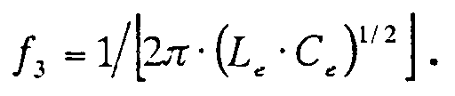
- the combined impedance Z of the first and third circuits for correcting frequency characteristics connected to the PD terminal is that of s ⁇ L d and s ⁇ Le + 1/(s ⁇ C e ) connected in parallel, whereby In this expression, in the low frequency region, only L d can be effective. As the frequency increases, on the other hand, Z is enhanced in a resonating fashion at Consequently, when suitable values of L e and C e are selected, L d can become equivalently greater in frequencies higher than f 1 . In order for the optical receiver to operate stably, however, it is necessary for the circuit as a whole to have no gain at any frequency between f 2 and
- avalanche diode and metal-semiconductor-metal (MSM) type devices may be used as light-receiving devices, and similar effects can be expected.
- MSM metal-semiconductor-metal
- circuits having an input impedance of 75 ohms, of course, a 50- ⁇ system circuit can be used.
- the gain can be appropriately improved in the frequency region higher than the cutoff frequency on the high frequency side in the conventional circuit, without affecting its middle to low frequency characteristics.
- a circuit technique can be employed to improve the high-frequency characteristics of an optical receiver.
Landscapes
- Engineering & Computer Science (AREA)
- Power Engineering (AREA)
- Physics & Mathematics (AREA)
- Electromagnetism (AREA)
- Computer Networks & Wireless Communication (AREA)
- Signal Processing (AREA)
- Amplifiers (AREA)
- Optical Communication System (AREA)
- Light Receiving Elements (AREA)
Abstract
Description


Claims (6)
- An optical receiver comprising a light-receiving device, having first and second terminals, for converting an optical input signal into an electric signal, the first terminal being coupled to a bias power supply; a preamplifier, coupled to the second terminal of said light-receiving device, for amplifying said electric signal; and an impedance-matching transformer, electrically coupled to said light-receiving device and said preamplifier, said impedance-matching transformer having a primary side impedance matching an output impedance of said light-receiving device and a secondary side impedance matching an input impedance of said preamplifier,
said optical receiver further comprising a first frequency characteristic compensating circuit, said first frequency characteristic compensating circuit being coupled between said bias power supply and the first terminal of said light-receiving device. - An optical receiver according to claim 1, further comprising a second frequency characteristic compensating circuit, said second frequency characteristic compensating circuit being coupled between said light-receiving device and said impedance-matching transformer.
- An optical receiver according to claim 1, wherein a junction between said first frequency characteristic compensating circuit and said light-receiving device is grounded by way of a third frequency characteristic compensating circuit.
- An optical receiver according to claim 2, wherein a junction between said first frequency characteristic compensating circuit and said light-receiving device is grounded by way of a third frequency characteristic compensating circuit.
- An optical receiver according to claim 3 or 4, wherein said third frequency characteristic compensating circuit comprises a serial circuit comprising a coil and a capacitor.
- An optical receiver according to any of claims 1 to 4, wherein each of said first frequency characteristic compensating circuit and said second frequency characteristic compensating circuit comprises a coil.
Applications Claiming Priority (3)
| Application Number | Priority Date | Filing Date | Title |
|---|---|---|---|
| JP159574/96 | 1996-06-20 | ||
| JP15957496A JP3858304B2 (en) | 1996-06-20 | 1996-06-20 | Optical receiver circuit |
| PCT/JP1997/002134 WO1997049205A1 (en) | 1996-06-20 | 1997-06-20 | Optical receiver |
Publications (3)
| Publication Number | Publication Date |
|---|---|
| EP0909044A1 true EP0909044A1 (en) | 1999-04-14 |
| EP0909044A4 EP0909044A4 (en) | 2005-06-15 |
| EP0909044B1 EP0909044B1 (en) | 2006-08-09 |
Family
ID=15696694
Family Applications (1)
| Application Number | Title | Priority Date | Filing Date |
|---|---|---|---|
| EP97927408A Expired - Lifetime EP0909044B1 (en) | 1996-06-20 | 1997-06-20 | Optical receiver |
Country Status (5)
| Country | Link |
|---|---|
| US (1) | US6410902B1 (en) |
| EP (1) | EP0909044B1 (en) |
| JP (1) | JP3858304B2 (en) |
| DE (1) | DE69736473T2 (en) |
| WO (1) | WO1997049205A1 (en) |
Cited By (3)
| Publication number | Priority date | Publication date | Assignee | Title |
|---|---|---|---|---|
| EP1560330A1 (en) * | 2004-02-02 | 2005-08-03 | Harman Becker Automotive Systems GmbH | Optical detector circuit |
| EP1826927A1 (en) * | 2006-01-27 | 2007-08-29 | OpNext Japan, Inc. | Optical receiver module |
| EP2312748A1 (en) * | 2009-10-19 | 2011-04-20 | CSEM Centre Suisse D'electronique Et De Microtechnique SA | System for detecting high-frequency narrowband signals |
Families Citing this family (9)
| Publication number | Priority date | Publication date | Assignee | Title |
|---|---|---|---|---|
| KR100682993B1 (en) | 2004-12-13 | 2007-02-15 | 한국전자통신연구원 | Optical Receiving Device Using Transformer |
| US7547872B2 (en) * | 2005-02-14 | 2009-06-16 | Ecole Polytechnique Federale De Lausanne | Integrated circuit comprising an array of single photon avalanche diodes |
| US20070023616A1 (en) * | 2005-07-29 | 2007-02-01 | Sauer Jeffrey L | Signal Detection System |
| CN100413078C (en) * | 2005-09-21 | 2008-08-20 | 天津大学 | CMOS photoelectric integrated receiver with pre-equalization circuit |
| JP2008282922A (en) * | 2007-05-09 | 2008-11-20 | Hochiki Corp | Photoelectric conversion device |
| JP5271391B2 (en) * | 2011-07-11 | 2013-08-21 | ホーチキ株式会社 | Photoelectric conversion device |
| JP5983200B2 (en) * | 2012-08-31 | 2016-08-31 | 富士通株式会社 | Optical module |
| JP2021044437A (en) * | 2019-09-12 | 2021-03-18 | 住友電気工業株式会社 | Light receiving device |
| CN115694660B (en) * | 2022-09-13 | 2023-09-22 | 北京无线电测量研究所 | T-shaped matching resonance enhanced photoelectric detector receiving network |
Family Cites Families (9)
| Publication number | Priority date | Publication date | Assignee | Title |
|---|---|---|---|---|
| US5089787A (en) * | 1985-05-05 | 1992-02-18 | California Institute Of Technology | Optically-coupled high frequency amplifier |
| DE4036411A1 (en) * | 1990-11-15 | 1992-05-21 | Standard Elektrik Lorenz Ag | OPTICAL RECEIVER |
| US5194979A (en) * | 1991-06-07 | 1993-03-16 | Gte Laboratories Incorporated | Wideband optical amplifier-receiver system |
| JPH06164253A (en) * | 1992-11-16 | 1994-06-10 | Matsushita Electric Ind Co Ltd | Optical receiver circuit |
| JPH06216663A (en) * | 1993-01-14 | 1994-08-05 | Sumitomo Electric Ind Ltd | Optical receiver |
| JPH06284090A (en) * | 1993-03-24 | 1994-10-07 | Sumitomo Electric Ind Ltd | Optical receiver |
| JPH06291293A (en) * | 1993-04-01 | 1994-10-18 | Hitachi Ltd | Optical receiver module |
| BE1007216A3 (en) * | 1993-06-11 | 1995-04-25 | Philips Electronics Nv | OPTICAL TRANSMISSION SYSTEM. |
| JP3200320B2 (en) * | 1994-09-27 | 2001-08-20 | 日本電信電話株式会社 | Light receiving circuit |
-
1996
- 1996-06-20 JP JP15957496A patent/JP3858304B2/en not_active Expired - Fee Related
-
1997
- 1997-06-20 WO PCT/JP1997/002134 patent/WO1997049205A1/en not_active Ceased
- 1997-06-20 US US09/214,405 patent/US6410902B1/en not_active Expired - Fee Related
- 1997-06-20 DE DE69736473T patent/DE69736473T2/en not_active Expired - Lifetime
- 1997-06-20 EP EP97927408A patent/EP0909044B1/en not_active Expired - Lifetime
Cited By (6)
| Publication number | Priority date | Publication date | Assignee | Title |
|---|---|---|---|---|
| EP1560330A1 (en) * | 2004-02-02 | 2005-08-03 | Harman Becker Automotive Systems GmbH | Optical detector circuit |
| US9083285B2 (en) | 2004-02-02 | 2015-07-14 | Harman Becker Automotive Systems Gmbh | Optical detector system |
| EP1826927A1 (en) * | 2006-01-27 | 2007-08-29 | OpNext Japan, Inc. | Optical receiver module |
| US7894726B2 (en) | 2006-01-27 | 2011-02-22 | Opnext Japan, Inc. | Optical receiver module |
| EP2312748A1 (en) * | 2009-10-19 | 2011-04-20 | CSEM Centre Suisse D'electronique Et De Microtechnique SA | System for detecting high-frequency narrowband signals |
| WO2011047492A1 (en) | 2009-10-19 | 2011-04-28 | Csem Centre Suisse D'electronique Et De Microtechnique S.A. | System for detecting high-frequency, narrow-band signals |
Also Published As
| Publication number | Publication date |
|---|---|
| JP3858304B2 (en) | 2006-12-13 |
| US6410902B1 (en) | 2002-06-25 |
| DE69736473T2 (en) | 2007-03-15 |
| EP0909044B1 (en) | 2006-08-09 |
| WO1997049205A1 (en) | 1997-12-24 |
| DE69736473D1 (en) | 2006-09-21 |
| EP0909044A4 (en) | 2005-06-15 |
| JPH1013360A (en) | 1998-01-16 |
Similar Documents
| Publication | Publication Date | Title |
|---|---|---|
| US6410902B1 (en) | Optical receiver | |
| US6639461B1 (en) | Ultra-wideband power amplifier module apparatus and method for optical and electronic communications | |
| US5042084A (en) | Three wire system for Cochlear implant processor | |
| US20090285579A1 (en) | Linearized trans-impedance amplifiers | |
| EP0702436B1 (en) | Laser package having an impedance matching transformer | |
| EP0469143B1 (en) | Push-pull optical receiver | |
| EP0836203B1 (en) | Amplifying unit comprising an input transformer capable of contributing to a wider frequency band of a broadband amplifier | |
| JP2003134051A (en) | Optical receiving module, optical receiver and optical fiber communication equipment | |
| US5517035A (en) | Broadband optical receiver with transformer coupled input circuit which is balanced to minimize stray capacitances | |
| US5471492A (en) | Broadband matching network | |
| US9614575B2 (en) | Direct coupled radio frequency (RF) transceiver front end | |
| US5982793A (en) | Semiconductor laser module with internal matching circuit | |
| EP0372742B1 (en) | Broadband optical receiver | |
| US5907422A (en) | Universal optical signal receiver | |
| CN112425100A (en) | Optical receiving circuit, optical receiver, optical terminal device, and optical communication system | |
| WO2000060694A1 (en) | A balun for coaxial cable transmission | |
| US6445743B1 (en) | Transmitting-receiving station having impedance-matched receiving means for transponder answer signals | |
| US5229599A (en) | Amplifying circuit arrangement with a signal source having a hi-ohmic output impedance | |
| US6572287B1 (en) | Assembly of an impedance transformer and a balun transformer | |
| KR100682993B1 (en) | Optical Receiving Device Using Transformer | |
| JPH06284090A (en) | Optical receiver | |
| JPH10233741A (en) | Optical receiver | |
| JPH09307173A (en) | Semiconductor laser module | |
| KR950009770Y1 (en) | High freq signal distribution apparatus | |
| JPH04329037A (en) | Analog light receiving element |
Legal Events
| Date | Code | Title | Description |
|---|---|---|---|
| PUAI | Public reference made under article 153(3) epc to a published international application that has entered the european phase |
Free format text: ORIGINAL CODE: 0009012 |
|
| 17P | Request for examination filed |
Effective date: 19990114 |
|
| AK | Designated contracting states |
Kind code of ref document: A1 Designated state(s): DE GB |
|
| A4 | Supplementary search report drawn up and despatched |
Effective date: 20050503 |
|
| RIC1 | Information provided on ipc code assigned before grant |
Ipc: 7H 03F 3/08 B Ipc: 7H 03H 7/38 B Ipc: 7H 04B 10/158 B Ipc: 7H 01L 31/10 A |
|
| RIC1 | Information provided on ipc code assigned before grant |
Ipc: 7H 03F 3/08 B Ipc: 7H 03H 7/38 B Ipc: 7H 04B 10/158 B Ipc: 7H 01L 31/10 B Ipc: 7H 04B 10/10 A |
|
| GRAP | Despatch of communication of intention to grant a patent |
Free format text: ORIGINAL CODE: EPIDOSNIGR1 |
|
| GRAS | Grant fee paid |
Free format text: ORIGINAL CODE: EPIDOSNIGR3 |
|
| GRAA | (expected) grant |
Free format text: ORIGINAL CODE: 0009210 |
|
| AK | Designated contracting states |
Kind code of ref document: B1 Designated state(s): DE GB |
|
| REG | Reference to a national code |
Ref country code: GB Ref legal event code: FG4D |
|
| REF | Corresponds to: |
Ref document number: 69736473 Country of ref document: DE Date of ref document: 20060921 Kind code of ref document: P |
|
| PLBE | No opposition filed within time limit |
Free format text: ORIGINAL CODE: 0009261 |
|
| STAA | Information on the status of an ep patent application or granted ep patent |
Free format text: STATUS: NO OPPOSITION FILED WITHIN TIME LIMIT |
|
| 26N | No opposition filed |
Effective date: 20070510 |
|
| PGFP | Annual fee paid to national office [announced via postgrant information from national office to epo] |
Ref country code: GB Payment date: 20110615 Year of fee payment: 15 |
|
| PGFP | Annual fee paid to national office [announced via postgrant information from national office to epo] |
Ref country code: DE Payment date: 20110615 Year of fee payment: 15 |
|
| GBPC | Gb: european patent ceased through non-payment of renewal fee |
Effective date: 20120620 |
|
| REG | Reference to a national code |
Ref country code: DE Ref legal event code: R119 Ref document number: 69736473 Country of ref document: DE Effective date: 20130101 |
|
| PG25 | Lapsed in a contracting state [announced via postgrant information from national office to epo] |
Ref country code: GB Free format text: LAPSE BECAUSE OF NON-PAYMENT OF DUE FEES Effective date: 20120620 Ref country code: DE Free format text: LAPSE BECAUSE OF NON-PAYMENT OF DUE FEES Effective date: 20130101 |