EP0908917A2 - Secondary emission coating for photomultiplier tubes - Google Patents
Secondary emission coating for photomultiplier tubes Download PDFInfo
- Publication number
- EP0908917A2 EP0908917A2 EP98308254A EP98308254A EP0908917A2 EP 0908917 A2 EP0908917 A2 EP 0908917A2 EP 98308254 A EP98308254 A EP 98308254A EP 98308254 A EP98308254 A EP 98308254A EP 0908917 A2 EP0908917 A2 EP 0908917A2
- Authority
- EP
- European Patent Office
- Prior art keywords
- substrate
- secondary electron
- diamond
- diamond film
- dynode
- Prior art date
- Legal status (The legal status is an assumption and is not a legal conclusion. Google has not performed a legal analysis and makes no representation as to the accuracy of the status listed.)
- Granted
Links
- 238000000576 coating method Methods 0.000 title claims description 5
- 239000011248 coating agent Substances 0.000 title claims description 3
- 229910003460 diamond Inorganic materials 0.000 claims abstract description 37
- 239000010432 diamond Substances 0.000 claims abstract description 37
- 239000000758 substrate Substances 0.000 claims abstract description 18
- 229910052783 alkali metal Inorganic materials 0.000 claims description 9
- 150000001340 alkali metals Chemical class 0.000 claims description 9
- 239000002019 doping agent Substances 0.000 claims description 6
- 238000000034 method Methods 0.000 claims description 6
- 238000004519 manufacturing process Methods 0.000 claims description 5
- ZOXJGFHDIHLPTG-UHFFFAOYSA-N Boron Chemical compound [B] ZOXJGFHDIHLPTG-UHFFFAOYSA-N 0.000 claims description 4
- ZOKXTWBITQBERF-UHFFFAOYSA-N Molybdenum Chemical compound [Mo] ZOKXTWBITQBERF-UHFFFAOYSA-N 0.000 claims description 4
- 229910052796 boron Inorganic materials 0.000 claims description 4
- 229910052750 molybdenum Inorganic materials 0.000 claims description 4
- 239000011733 molybdenum Substances 0.000 claims description 4
- 229910052751 metal Inorganic materials 0.000 claims description 3
- 239000002184 metal Substances 0.000 claims description 3
- 239000003870 refractory metal Substances 0.000 claims description 2
- 229910052715 tantalum Inorganic materials 0.000 claims description 2
- GUVRBAGPIYLISA-UHFFFAOYSA-N tantalum atom Chemical compound [Ta] GUVRBAGPIYLISA-UHFFFAOYSA-N 0.000 claims description 2
- WFKWXMTUELFFGS-UHFFFAOYSA-N tungsten Chemical compound [W] WFKWXMTUELFFGS-UHFFFAOYSA-N 0.000 claims description 2
- 229910052721 tungsten Inorganic materials 0.000 claims description 2
- 239000010937 tungsten Substances 0.000 claims description 2
- 231100001261 hazardous Toxicity 0.000 description 4
- 239000000463 material Substances 0.000 description 4
- 229910005540 GaP Inorganic materials 0.000 description 3
- 229910052787 antimony Inorganic materials 0.000 description 3
- WATWJIUSRGPENY-UHFFFAOYSA-N antimony atom Chemical compound [Sb] WATWJIUSRGPENY-UHFFFAOYSA-N 0.000 description 3
- 239000002585 base Substances 0.000 description 3
- 229910052799 carbon Inorganic materials 0.000 description 3
- 238000002059 diagnostic imaging Methods 0.000 description 3
- HZXMRANICFIONG-UHFFFAOYSA-N gallium phosphide Chemical compound [Ga]#P HZXMRANICFIONG-UHFFFAOYSA-N 0.000 description 3
- 239000007789 gas Substances 0.000 description 3
- OKTJSMMVPCPJKN-UHFFFAOYSA-N Carbon Chemical compound [C] OKTJSMMVPCPJKN-UHFFFAOYSA-N 0.000 description 2
- 238000001994 activation Methods 0.000 description 2
- 239000003513 alkali Substances 0.000 description 2
- 230000009286 beneficial effect Effects 0.000 description 2
- 230000008901 benefit Effects 0.000 description 2
- 238000005229 chemical vapour deposition Methods 0.000 description 2
- 239000011521 glass Substances 0.000 description 2
- 238000011065 in-situ storage Methods 0.000 description 2
- 150000001247 metal acetylides Chemical class 0.000 description 2
- 230000005855 radiation Effects 0.000 description 2
- 230000035945 sensitivity Effects 0.000 description 2
- 238000007725 thermal activation Methods 0.000 description 2
- 239000004215 Carbon black (E152) Substances 0.000 description 1
- DGAQECJNVWCQMB-PUAWFVPOSA-M Ilexoside XXIX Chemical compound C[C@@H]1CC[C@@]2(CC[C@@]3(C(=CC[C@H]4[C@]3(CC[C@@H]5[C@@]4(CC[C@@H](C5(C)C)OS(=O)(=O)[O-])C)C)[C@@H]2[C@]1(C)O)C)C(=O)O[C@H]6[C@@H]([C@H]([C@@H]([C@H](O6)CO)O)O)O.[Na+] DGAQECJNVWCQMB-PUAWFVPOSA-M 0.000 description 1
- ZLMJMSJWJFRBEC-UHFFFAOYSA-N Potassium Chemical compound [K] ZLMJMSJWJFRBEC-UHFFFAOYSA-N 0.000 description 1
- 238000009825 accumulation Methods 0.000 description 1
- 230000004913 activation Effects 0.000 description 1
- 230000015572 biosynthetic process Effects 0.000 description 1
- -1 butane Chemical class 0.000 description 1
- 239000001273 butane Substances 0.000 description 1
- 229910052792 caesium Inorganic materials 0.000 description 1
- TVFDJXOCXUVLDH-UHFFFAOYSA-N caesium atom Chemical compound [Cs] TVFDJXOCXUVLDH-UHFFFAOYSA-N 0.000 description 1
- 238000001816 cooling Methods 0.000 description 1
- 230000002950 deficient Effects 0.000 description 1
- 238000000151 deposition Methods 0.000 description 1
- 230000008021 deposition Effects 0.000 description 1
- 238000005137 deposition process Methods 0.000 description 1
- 238000001514 detection method Methods 0.000 description 1
- 230000000694 effects Effects 0.000 description 1
- 150000004820 halides Chemical class 0.000 description 1
- 229930195733 hydrocarbon Natural products 0.000 description 1
- 150000002430 hydrocarbons Chemical class 0.000 description 1
- 238000003384 imaging method Methods 0.000 description 1
- 238000005259 measurement Methods 0.000 description 1
- 150000002739 metals Chemical class 0.000 description 1
- IJDNQMDRQITEOD-UHFFFAOYSA-N n-butane Chemical compound CCCC IJDNQMDRQITEOD-UHFFFAOYSA-N 0.000 description 1
- OFBQJSOFQDEBGM-UHFFFAOYSA-N n-pentane Natural products CCCCC OFBQJSOFQDEBGM-UHFFFAOYSA-N 0.000 description 1
- 229910052700 potassium Inorganic materials 0.000 description 1
- 239000011591 potassium Substances 0.000 description 1
- 229910052701 rubidium Inorganic materials 0.000 description 1
- IGLNJRXAVVLDKE-UHFFFAOYSA-N rubidium atom Chemical compound [Rb] IGLNJRXAVVLDKE-UHFFFAOYSA-N 0.000 description 1
- 229910052708 sodium Inorganic materials 0.000 description 1
- 239000011734 sodium Substances 0.000 description 1
- 239000000126 substance Substances 0.000 description 1
Images
Classifications
-
- H—ELECTRICITY
- H01—ELECTRIC ELEMENTS
- H01J—ELECTRIC DISCHARGE TUBES OR DISCHARGE LAMPS
- H01J43/00—Secondary-emission tubes; Electron-multiplier tubes
- H01J43/04—Electron multipliers
- H01J43/06—Electrode arrangements
- H01J43/10—Dynodes
-
- H—ELECTRICITY
- H01—ELECTRIC ELEMENTS
- H01J—ELECTRIC DISCHARGE TUBES OR DISCHARGE LAMPS
- H01J1/00—Details of electrodes, of magnetic control means, of screens, or of the mounting or spacing thereof, common to two or more basic types of discharge tubes or lamps
- H01J1/02—Main electrodes
- H01J1/32—Secondary-electron-emitting electrodes
Definitions
- This invention deals generally with electron discharge devices, and more specifically with a secondary electron emitting surface constructed with diamond film and used in photomultiplier tubes.
- Photomultiplier tubes have become commonly used for detecting low radiation levels.
- Typical such tubes consist of a glass envelope with an electron emitting photocathode located on the inside surface of a faceplate on the envelope. When radiation strikes the photocathode, electrons emitted from it are directed toward and collected by an electron multiplier.
- the electron multiplier consists of several dynodes with secondary electron emitting surfaces, with the first dynode receiving the electrons from the photocathode.
- the electron multiplier has an electrical output which is directly related to the quantity of electrons collected by the first dynode, and increasing the ratio of the quantity of electrons at the output of the electron multiplier to the quantity of the electrons received by the first dynode is a continuing design goal. This ratio is largely determined by the gain of the individual dynodes, expressed in a simple number ratio, which indicates the number of secondary electrons emitted for every electron striking the dynode secondary emitter surfaces.
- gallium phosphide requires special thermal activation in a vacuum during tube processing and it also requires the use of hazardous gases during its processing.
- the present invention furnishes a modified diamond layer, a diamond layer with p-doping, applied to a standard substrate, preferably of molybdenum, for use as a secondary emitter in photomultiplier tube dynodes.
- the diamond layer is p-doped with boron.
- the p-doped diamond layer provide higher gain, but a substantial additional advantage of such a p-doped diamond secondary emitter layer is that it has lower hysteresis and greater pulse rate stability than prior art secondary emitters, even the undoped diamond emitters.
- the p-doped diamond film of the invention can also be placed on the substrate before being put into the tube.
- antimony in-situ Such antimony coating are applied from special sources installed in the tube which are activated while the tubes are being processed on the exhaust system. This method results in high secondary emission in the first dynode position, but since the antimony is evaporated in-situ, it is not uniform and hence can have a negative effect on pulse height resolution and sensitivity to external magnetic fields.
- Gallium phosphide dynodes which also provide exceptionally high secondary emission, require a hazardous fabrication process and require thermal activation during the exhaust process. Diamond deposition is not a hazardous process, and the dynodes do not require any special activation process.
- the invention thereby provides a secondary electron emitter surface for use in photomultiplier tubes with a gain equivalent to or greater than the prior art devices and with superior stability, but the surface is easier and less hazardous to manufacture.
- the high secondary emission p-doped diamond layer dynode of the present invention can be used in various applications.
- tubes are designed with large, high collection and high gain dynodes at the front end of the tubes. This lends itself to improved pulse height resolution, an important parameter for scintillation detection.
- P-doped diamond coated dynodes are uniform over large areas with secondary emission, and that satisfies such design criteria.
- the applications for p-doped diamond coated dynodes can also be extended to latter stages of the electron multiplier.
- the higher gain of the dynode results in a lower number of dynodes required to achieve the desired tube gain.
- Electron multipliers with fewer stages require less physical space, leading to more compact and less massive imaging systems, a benefit in both medical imaging technology and photon counting applications.
- the invention also provides a complete photomultiplier tube as well as a method for its manufacture as defined in the annexed claims.
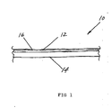
- FIGURE is a simplified drawing of the preferred embodiment of the secondary emitting surface of the invention.
- the FIGURE is a drawing of the very simple preferred embodiment of the invention in which secondary emitter 10 is formed only from p-doped diamond film 12 coated by chemical vapor deposition upon base substrate 14.
- Alkali metal layer 16 is then conventionally produced upon p-doped diamond film 12 during the generation of the photocathode within the tube.
- the alkali metal layer may be caesium, potassium, sodium, or rubidium for example. This layer may be produced after assembly of the photomultiplier tube or other devices in which the invention is used. In this case, the device is assembled with untreated diamond dynode surfaces.
- the device enclosed in a glass or metal envelope is evacuated, and any of the above mentioned alkali is introduced in its metallic form at a temperature, 150°C to 250°C, where the metals exist as a vapour.
- the alkali metals deposit on the dynode surfaces yielding an activated diamond surface with high secondary emission. It should be recognised that even at higher temperatures, alkali metal will still be present on the dynode surface, maintaining its activation.
- Base substrate 14 is selected from materials that promote the growth of tetrahedrally coordinated or sp3 carbon, such as refractory metals (e.g. molybdenum, tungsten, tantalum) or other carbide formers. These materials react with carbon to form carbides. These carbides have a molecular structure or chemical bonding geometry similar to that of diamond, and so the formation of such a carbide at the substrate surface promotes the growth of diamond. In addition, the thermal expansion of, for example, molybdenum is close to that of diamond, minimising interfacial stresses that might cause the diamond to separate from the substrate.
- refractory metals e.g. molybdenum, tungsten, tantalum
- Conventional substrate 14 is typically .005 inch thick and p-doped diamond film 12 is 1-10 microns thick.
- P-doped diamond or diamond-like-carbon film 12 is typically applied to base substrate 14 by chemical vapor deposition or plasma deposition processes.
- the microstructure of the film is polycrystalline, exposing facets of a preferred crystallographic plane.
- the p-dopant is typically boron, and the dopant level is such that the modified resistivity of the diamond film is in the range between 600 and 1600 ohm/square.
- the diamond is grown from the gas phase using a hydrocarbon such as butane, and the gas BH 3 is simultaneously admitted to the growth chamber in the appropriate amount so as to generate the desired doping level.
- a hydrocarbon such as butane
- Secondary emitter 10 of the FIGURE can be completely prepared and processed outside the tube in which it will be used after substrate 14 is first shaped into the appropriate dynode surface, and then, after the dynode is installed within a tube, tube processing can proceed as usual.
- secondary emitter 10 of the preferred embodiment of the invention When tested as a photomultiplier dynode, secondary emitter 10 of the preferred embodiment of the invention demonstrated that its gain is almost linear with incident beam energy, with gains of 29 at 600 volts and 48 at 1000 volts. Such a high first dynode gain results in improved pulse height resolution in tubes used for medical imaging applications.
- p-dopants may be sued instead of boron, and, of course, other materials may be used for the substrate.
Landscapes
- Crystals, And After-Treatments Of Crystals (AREA)
- Common Detailed Techniques For Electron Tubes Or Discharge Tubes (AREA)
- Formation Of Various Coating Films On Cathode Ray Tubes And Lamps (AREA)
Abstract
Description
Claims (8)
- A photomultiplier tube dynode secondary electron emitter comprising a substrate and a diamond film on the substrate wherein the diamond film includes a p-dopant.
- A secondary electron emitter according to claim 1 further including an alkali metal coating on the diamond film.
- A secondary electron emitter according to claim 1 or 2 wherein the p-dopant is boron.
- A secondary electron emitter according to any preceding claim wherein the substrate is a refractory metal.
- A secondary electron emitter according to claim 4 wherein the substrate is molybdenum, tungsten, or tantalum.
- A secondary electron emitter according to any preceding claim wherein the quantity of p-dopant within the diamond film is sufficient to make the resistivity of the diamond film in the range of between 600 and 1600 ohm/square.
- A photomultiplier tube having at least one secondary electron emitter as claimed in any preceding claim.
- Method for manufacturing a photomultiplier tube having at least one dynode secondary emitter comprising a p-doped diamond film formed on a substrate, wherein the tube is enclosed in an envelope, the envelope is evacuated and an alkali metal is introduced at a temperature such that the metal is in vapour form.
Applications Claiming Priority (2)
| Application Number | Priority Date | Filing Date | Title |
|---|---|---|---|
| US94749797A | 1997-10-10 | 1997-10-10 | |
| US947497 | 1997-10-10 |
Publications (3)
| Publication Number | Publication Date |
|---|---|
| EP0908917A2 true EP0908917A2 (en) | 1999-04-14 |
| EP0908917A3 EP0908917A3 (en) | 2000-03-22 |
| EP0908917B1 EP0908917B1 (en) | 2005-04-20 |
Family
ID=25486238
Family Applications (1)
| Application Number | Title | Priority Date | Filing Date |
|---|---|---|---|
| EP98308254A Expired - Lifetime EP0908917B1 (en) | 1997-10-10 | 1998-10-09 | Secondary emission coating for photomultiplier tubes |
Country Status (2)
| Country | Link |
|---|---|
| EP (1) | EP0908917B1 (en) |
| DE (1) | DE69829816T2 (en) |
Cited By (5)
| Publication number | Priority date | Publication date | Assignee | Title |
|---|---|---|---|---|
| WO2005006734A1 (en) * | 2003-07-09 | 2005-01-20 | Council For The Central Laboratory Of The Research Councils | Image machine using a large area electron multiplier |
| EP1400293A3 (en) * | 2002-07-16 | 2006-04-12 | Seco Tools Ab | PVD coated cutting tool |
| WO2011157810A1 (en) * | 2010-06-18 | 2011-12-22 | Photonis France | Electron multiplier detector formed from a highly doped nanodiamond layer |
| FR2964785A1 (en) * | 2010-09-13 | 2012-03-16 | Photonis France | ELECTRON MULTIPLIER DEVICE WITH NANODIAMANT LAYER. |
| WO2020227785A1 (en) * | 2019-05-16 | 2020-11-19 | Adaptas Solutions Pty Ltd | Improved reflection mode dynode |
Family Cites Families (3)
| Publication number | Priority date | Publication date | Assignee | Title |
|---|---|---|---|---|
| DE69030145T2 (en) * | 1989-08-18 | 1997-07-10 | Galileo Electro Optics Corp | Continuous thin film dynodes |
| US5619091A (en) * | 1994-10-03 | 1997-04-08 | Universities Research Association, Inc. | Diamond films treated with alkali-halides |
| US5886465A (en) * | 1996-09-26 | 1999-03-23 | Hamamatsu Photonics K.K. | Photomultiplier tube with multi-layer anode and final stage dynode |
-
1998
- 1998-10-09 EP EP98308254A patent/EP0908917B1/en not_active Expired - Lifetime
- 1998-10-09 DE DE69829816T patent/DE69829816T2/en not_active Expired - Lifetime
Cited By (11)
| Publication number | Priority date | Publication date | Assignee | Title |
|---|---|---|---|---|
| EP1400293A3 (en) * | 2002-07-16 | 2006-04-12 | Seco Tools Ab | PVD coated cutting tool |
| WO2005006734A1 (en) * | 2003-07-09 | 2005-01-20 | Council For The Central Laboratory Of The Research Councils | Image machine using a large area electron multiplier |
| WO2011157810A1 (en) * | 2010-06-18 | 2011-12-22 | Photonis France | Electron multiplier detector formed from a highly doped nanodiamond layer |
| FR2961628A1 (en) * | 2010-06-18 | 2011-12-23 | Photonis France | ELECTRON MULTIPLIER DETECTOR FORMED OF A HIGHLY DOPED NANODIAMANT LAYER |
| US9035540B2 (en) | 2010-06-18 | 2015-05-19 | Photonis France | Electron multiplier detector formed from a highly doped nanodiamond layer |
| FR2964785A1 (en) * | 2010-09-13 | 2012-03-16 | Photonis France | ELECTRON MULTIPLIER DEVICE WITH NANODIAMANT LAYER. |
| WO2012034948A1 (en) * | 2010-09-13 | 2012-03-22 | Photonis France | Electron multiplier device having a nanodiamond layer |
| US8912526B2 (en) | 2010-09-13 | 2014-12-16 | Photonis France | Electron multiplier device having a nanodiamond layer |
| WO2020227785A1 (en) * | 2019-05-16 | 2020-11-19 | Adaptas Solutions Pty Ltd | Improved reflection mode dynode |
| CN114072893A (en) * | 2019-05-16 | 2022-02-18 | 艾德特斯解决方案有限公司 | Improved reflection mode dynode |
| US12198915B2 (en) | 2019-05-16 | 2025-01-14 | Adaptas Solutions Pty Ltd | Reflection mode dynode |
Also Published As
| Publication number | Publication date |
|---|---|
| DE69829816D1 (en) | 2005-05-25 |
| EP0908917A3 (en) | 2000-03-22 |
| EP0908917B1 (en) | 2005-04-20 |
| DE69829816T2 (en) | 2006-01-26 |
Similar Documents
| Publication | Publication Date | Title |
|---|---|---|
| US5680008A (en) | Compact low-noise dynodes incorporating semiconductor secondary electron emitting materials | |
| US8686733B2 (en) | Ionization gauge having electron multiplier cold emission source | |
| KR101907223B1 (en) | Electron multiplier device having a nanodiamond layer | |
| US5378960A (en) | Thin film continuous dynodes for electron multiplication | |
| US6566884B2 (en) | Ionization vacuum pressure gauge | |
| Plumlee et al. | Mass Spectrometric Study of Solids I. Preliminary Study of Sublimation Characteristics of Oxide Cathode Materials | |
| US8410433B2 (en) | Mass spectrometer | |
| EP0908917B1 (en) | Secondary emission coating for photomultiplier tubes | |
| EP1260616A1 (en) | Polycrystalline diamond thin film, photocathode and electron tube using it | |
| US6670752B2 (en) | Cathode for emitting photoelectron or secondary electron, photomultiplier tube, and electron-multiplier tube | |
| US5619091A (en) | Diamond films treated with alkali-halides | |
| JPH0244639A (en) | Manufacture of photoelectric doubler tube | |
| US12198915B2 (en) | Reflection mode dynode | |
| US4407857A (en) | Method for processing a lithium-sodium-antimony photocathode | |
| US11901169B2 (en) | Barrier coatings | |
| US20240136139A1 (en) | A uv sensitive photocathode, a method for producing a uv sensitive photocathode, and a detector for measuring uv radiation | |
| JPH11120899A (en) | Secondary electron discharge device and electron tube using the device | |
| Mackie et al. | Emission and processing requirements for carbide films on Mo field emitters | |
| GB2040553A (en) | Dynode | |
| Anderson et al. | Diamond films treated with alkali-halides | |
| Testerman et al. | Cold Electron Sources for Mass Spectrometric Applications | |
| HK40065143A (en) | Improved reflection mode dynode | |
| Vroom et al. | Cross sections for charge transfer between mercury ions and other metals | |
| Koryukin | Change in the properties of the electrodes of thermionic single-element EGC at the initial stage of operation | |
| Warshawsky | Classified abstracts 6094-6102 |
Legal Events
| Date | Code | Title | Description |
|---|---|---|---|
| PUAI | Public reference made under article 153(3) epc to a published international application that has entered the european phase |
Free format text: ORIGINAL CODE: 0009012 |
|
| AK | Designated contracting states |
Kind code of ref document: A2 Designated state(s): DE FR GB |
|
| AX | Request for extension of the european patent |
Free format text: AL;LT;LV;MK;RO;SI |
|
| PUAL | Search report despatched |
Free format text: ORIGINAL CODE: 0009013 |
|
| AK | Designated contracting states |
Kind code of ref document: A3 Designated state(s): AT BE CH CY DE DK ES FI FR GB GR IE IT LI LU MC NL PT SE |
|
| AX | Request for extension of the european patent |
Free format text: AL;LT;LV;MK;RO;SI |
|
| 17P | Request for examination filed |
Effective date: 20000728 |
|
| AKX | Designation fees paid |
Free format text: DE FR GB |
|
| 17Q | First examination report despatched |
Effective date: 20020626 |
|
| GRAP | Despatch of communication of intention to grant a patent |
Free format text: ORIGINAL CODE: EPIDOSNIGR1 |
|
| GRAS | Grant fee paid |
Free format text: ORIGINAL CODE: EPIDOSNIGR3 |
|
| GRAA | (expected) grant |
Free format text: ORIGINAL CODE: 0009210 |
|
| AK | Designated contracting states |
Kind code of ref document: B1 Designated state(s): DE FR GB |
|
| REG | Reference to a national code |
Ref country code: GB Ref legal event code: FG4D |
|
| REF | Corresponds to: |
Ref document number: 69829816 Country of ref document: DE Date of ref document: 20050525 Kind code of ref document: P |
|
| PLBE | No opposition filed within time limit |
Free format text: ORIGINAL CODE: 0009261 |
|
| STAA | Information on the status of an ep patent application or granted ep patent |
Free format text: STATUS: NO OPPOSITION FILED WITHIN TIME LIMIT |
|
| ET | Fr: translation filed | ||
| 26N | No opposition filed |
Effective date: 20060123 |
|
| REG | Reference to a national code |
Ref country code: FR Ref legal event code: PLFP Year of fee payment: 18 |
|
| REG | Reference to a national code |
Ref country code: FR Ref legal event code: PLFP Year of fee payment: 19 |
|
| REG | Reference to a national code |
Ref country code: FR Ref legal event code: PLFP Year of fee payment: 20 |
|
| PGFP | Annual fee paid to national office [announced via postgrant information from national office to epo] |
Ref country code: FR Payment date: 20171025 Year of fee payment: 20 Ref country code: DE Payment date: 20171027 Year of fee payment: 20 |
|
| PGFP | Annual fee paid to national office [announced via postgrant information from national office to epo] |
Ref country code: GB Payment date: 20171027 Year of fee payment: 20 |
|
| REG | Reference to a national code |
Ref country code: DE Ref legal event code: R071 Ref document number: 69829816 Country of ref document: DE |
|
| REG | Reference to a national code |
Ref country code: GB Ref legal event code: PE20 Expiry date: 20181008 |
|
| PG25 | Lapsed in a contracting state [announced via postgrant information from national office to epo] |
Ref country code: GB Free format text: LAPSE BECAUSE OF EXPIRATION OF PROTECTION Effective date: 20181008 |