EP0902512A2 - Integrated interferometric structure - Google Patents
Integrated interferometric structure Download PDFInfo
- Publication number
- EP0902512A2 EP0902512A2 EP98402199A EP98402199A EP0902512A2 EP 0902512 A2 EP0902512 A2 EP 0902512A2 EP 98402199 A EP98402199 A EP 98402199A EP 98402199 A EP98402199 A EP 98402199A EP 0902512 A2 EP0902512 A2 EP 0902512A2
- Authority
- EP
- European Patent Office
- Prior art keywords
- amplifier
- output
- optical
- signal
- amplifiers
- Prior art date
- Legal status (The legal status is an assumption and is not a legal conclusion. Google has not performed a legal analysis and makes no representation as to the accuracy of the status listed.)
- Withdrawn
Links
Images


Classifications
-
- H—ELECTRICITY
- H01—ELECTRIC ELEMENTS
- H01S—DEVICES USING THE PROCESS OF LIGHT AMPLIFICATION BY STIMULATED EMISSION OF RADIATION [LASER] TO AMPLIFY OR GENERATE LIGHT; DEVICES USING STIMULATED EMISSION OF ELECTROMAGNETIC RADIATION IN WAVE RANGES OTHER THAN OPTICAL
- H01S5/00—Semiconductor lasers
- H01S5/50—Amplifier structures not provided for in groups H01S5/02 - H01S5/30
-
- G—PHYSICS
- G02—OPTICS
- G02F—OPTICAL DEVICES OR ARRANGEMENTS FOR THE CONTROL OF LIGHT BY MODIFICATION OF THE OPTICAL PROPERTIES OF THE MEDIA OF THE ELEMENTS INVOLVED THEREIN; NON-LINEAR OPTICS; FREQUENCY-CHANGING OF LIGHT; OPTICAL LOGIC ELEMENTS; OPTICAL ANALOGUE/DIGITAL CONVERTERS
- G02F1/00—Devices or arrangements for the control of the intensity, colour, phase, polarisation or direction of light arriving from an independent light source, e.g. switching, gating or modulating; Non-linear optics
- G02F1/35—Non-linear optics
- G02F1/3515—All-optical modulation, gating, switching, e.g. control of a light beam by another light beam
- G02F1/3517—All-optical modulation, gating, switching, e.g. control of a light beam by another light beam using an interferometer
-
- G—PHYSICS
- G02—OPTICS
- G02F—OPTICAL DEVICES OR ARRANGEMENTS FOR THE CONTROL OF LIGHT BY MODIFICATION OF THE OPTICAL PROPERTIES OF THE MEDIA OF THE ELEMENTS INVOLVED THEREIN; NON-LINEAR OPTICS; FREQUENCY-CHANGING OF LIGHT; OPTICAL LOGIC ELEMENTS; OPTICAL ANALOGUE/DIGITAL CONVERTERS
- G02F1/00—Devices or arrangements for the control of the intensity, colour, phase, polarisation or direction of light arriving from an independent light source, e.g. switching, gating or modulating; Non-linear optics
- G02F1/01—Devices or arrangements for the control of the intensity, colour, phase, polarisation or direction of light arriving from an independent light source, e.g. switching, gating or modulating; Non-linear optics for the control of the intensity, phase, polarisation or colour
- G02F1/21—Devices or arrangements for the control of the intensity, colour, phase, polarisation or direction of light arriving from an independent light source, e.g. switching, gating or modulating; Non-linear optics for the control of the intensity, phase, polarisation or colour by interference
- G02F1/225—Devices or arrangements for the control of the intensity, colour, phase, polarisation or direction of light arriving from an independent light source, e.g. switching, gating or modulating; Non-linear optics for the control of the intensity, phase, polarisation or colour by interference in an optical waveguide structure
- G02F1/2257—Devices or arrangements for the control of the intensity, colour, phase, polarisation or direction of light arriving from an independent light source, e.g. switching, gating or modulating; Non-linear optics for the control of the intensity, phase, polarisation or colour by interference in an optical waveguide structure the optical waveguides being made of semiconducting material
-
- H—ELECTRICITY
- H01—ELECTRIC ELEMENTS
- H01S—DEVICES USING THE PROCESS OF LIGHT AMPLIFICATION BY STIMULATED EMISSION OF RADIATION [LASER] TO AMPLIFY OR GENERATE LIGHT; DEVICES USING STIMULATED EMISSION OF ELECTROMAGNETIC RADIATION IN WAVE RANGES OTHER THAN OPTICAL
- H01S5/00—Semiconductor lasers
- H01S5/02—Structural details or components not essential to laser action
- H01S5/026—Monolithically integrated components, e.g. waveguides, monitoring photo-detectors, drivers
-
- H—ELECTRICITY
- H01—ELECTRIC ELEMENTS
- H01S—DEVICES USING THE PROCESS OF LIGHT AMPLIFICATION BY STIMULATED EMISSION OF RADIATION [LASER] TO AMPLIFY OR GENERATE LIGHT; DEVICES USING STIMULATED EMISSION OF ELECTROMAGNETIC RADIATION IN WAVE RANGES OTHER THAN OPTICAL
- H01S5/00—Semiconductor lasers
- H01S5/06—Arrangements for controlling the laser output parameters, e.g. by operating on the active medium
- H01S5/0601—Arrangements for controlling the laser output parameters, e.g. by operating on the active medium comprising an absorbing region
-
- H—ELECTRICITY
- H01—ELECTRIC ELEMENTS
- H01S—DEVICES USING THE PROCESS OF LIGHT AMPLIFICATION BY STIMULATED EMISSION OF RADIATION [LASER] TO AMPLIFY OR GENERATE LIGHT; DEVICES USING STIMULATED EMISSION OF ELECTROMAGNETIC RADIATION IN WAVE RANGES OTHER THAN OPTICAL
- H01S5/00—Semiconductor lasers
- H01S5/10—Construction or shape of the optical resonator, e.g. extended or external cavity, coupled cavities, bent-guide, varying width, thickness or composition of the active region
- H01S5/1003—Waveguide having a modified shape along the axis, e.g. branched, curved, tapered, voids
Definitions
- the invention relates to systems optoelectronics used for optical transmission or the processing of optical digital data.
- the converters of wavelength are used to convert an optical signal transmitted, from one wavelength to another wavelength, while maintaining its performance.
- the information is under the form of binary data represented by pulses modulating an optical carrier wave.
- a binary value is therefore determined according to the level of amplitude (or power) of the modulated optical wave.
- this signal may be subject to degradations that make it more difficult, in terms of receivers, detecting high and low signal levels received.
- the quality of a signal optics is usually defined by at least two parameters: signal-to-noise ratio and rate of extinction.
- the signal-to-noise ratio is defined as the ratio from optical signal power to noise power in a wavelength band containing the length wave of the signal carrier.
- the extinction rate is defined as the ratio of powers corresponding respectively to the high levels and signal down. This rate must be high enough despite variations in the input signal.
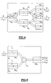
- An interferometric structure is shown in Figure 1 in the case of the wavelength converter. It consists of two guiding branches 1 and 2. At least one of these branches is provided with an OA semiconductor optical amplifier 1 . However, in general it is preferable to place a second semiconductor optical amplifier OA 2 on the other branch 2 for reasons of symmetry. Indeed, the presence of the second OA 2 semiconductor optical amplifier makes it possible to conserve substantially the same level of amplification in the two branches of the structure and consequently to have substantially identical powers at the output of the branches of the interferometer.
- optical amplifiers OA 1 , OA 2 are sufficient to form the interferometric structure when it is of the "active-passive" type, that is to say when the guides which compose it are produced from two types of material, for train active guides and passive guides.
- the guides located at the ends of the interferometric structure form passive guides and are made of a non-absorbent material so that the optical signal at the output of the interferometric structure is identical to the signal from the amplifiers OA 1 and OA 2 .
- the realization of such an integrated structure of the “active-passive” type is very complicated to implement because it requires several successive epitaxy recoveries to deposit the two types of material. The realization of this structure being long and tedious, its cost is considerably increased.
- all active that is to say a structure whose guides are all active and formed from a single material.
- the optical signal from the amplifiers OA 1 and OA 2 is strongly absorbed by the material used and the optical power at the output of the structure becomes far too weak to be detected. Consequently, in such an “all active” type structure, it is necessary to place peripheral optical amplifiers in order to amplify the optical power absorbed and to recover a suitable signal at the output of the structure.
- peripheral amplifiers are referenced OA 3 , OA 4 , OA 5 and OA 6 in Figure 1.
- a first coupler K 1 makes it possible to couple one end of each of these branches to a peripheral semiconductor optical amplifier, also called input amplifier OA 5 .
- a laser source 7 also makes it possible to supply, to this peripheral amplifier OA 5 , an output carrier wave M of wavelength ⁇ S.
- a second coupler K 2 is arranged so as to couple the other end of the first branch 1 to another optical semiconductor input peripheral amplifier OA 4 .
- This coupler K 2 allows the introduction into the first amplifier OA 1 of an input signal E of wavelength ⁇ e having been amplified by the input amplifier OA 4 .
- the amplifier OA 1 saturates and the state of the interferometer is changed, which causes a phase modulation of the output carrier wave.
- the waves AM 1 and AM 2 correspond to the waves M 1 and M 2 coming from the coupler K 1 and amplified respectively by the amplifiers OA 1 and OA 2 .
- the output signal S is then amplified by the peripheral output amplifier OA 3 .
- Another peripheral amplifier OA 6 is also provided to respect the symmetry of the structure and to allow the replacement of one of the amplifiers OA 3 or OA 4 in the event of a possible failure.
- the saturation power threshold of the amplifiers OA 1 and OA 2 located in the branches 1 and 2 of such an interferometric structure is set relatively low. Consequently, when the interference of the waves AM 1 and AM 2 is constructive, that is to say when the waves AM 1 and AM 2 are in phase, the optical powers of the two amplifiers OA 1 and OA 2 are added so well that the optical power in the output amplifier OA 3 is very high.
- the output amplifier OA 3 strongly saturates and the extinction rate is very degraded.
- the gain of the high levels becomes lower than the gain of the low levels, so that the output signal S undergoes compression of the high levels and is consequently distorted.
- This deformation can also occur on the input signal E, or on the output carrier wave M. Or, if the input signal E is deformed, or if the output carrier wave M is deformed, then the output signal S is also degraded and the rate of extinction of the interferometric structure is reduced.
- the saturation power input of an amplifier is defined by the power input optics for which the amplifier gain is divided by 2.
- the aforementioned drawbacks may appear in any "all active" interferometric structure.
- the object of the invention is to remedy these drawbacks by proposing a structure which, compared to structures known, makes the input saturation power of peripheral amplifiers more difficult to reach by the input power of these amplifiers. For that, we can either seek to increase the saturation power input of said amplifiers either do so that the input power of these amplifiers is scaled down.
- a structure interferometric integrated to provide an optical signal of output in which a first and a second branch, comprising at least a first semiconductor optical amplifier, are coupled to optical amplifiers input and / or output peripheral semiconductors, characterized in that said structure has a section attenuation between the output of at least one amplifier semiconductor optics of one of the branches and the input of the peripheral output amplifier and / or the length of the waveguide of at least one peripheral amplifier is less than 300 ⁇ m.
- the attenuation section brings at least 50% losses optical.
- the optical semiconductor amplifiers OA 1 and OA 2 situated on the branches of the interferometers of the Mach-Zehnder type or equivalent must have a relatively low saturation threshold.
- the peripheral amplifiers OA 3 should be , OA 4 and OA 5 operate in the lowest saturation regime possible.
- the structure must be such that the input saturation threshold is more difficult to reach by the input power.
- the operating conditions of at least one peripheral amplifier are modified. These operating conditions include the optical power at the input of the amplifier or its input saturation power. Preferably, it is the operating conditions of the output amplifier that are first modified. The operating conditions of the other peripheral amplifiers OA 4 then OA 5 can then be modified to avoid any distortion of the input signal E of the output carrier wave M.
- a first embodiment of a wavelength converter according to the invention consists in enabling the optical power injected into the peripheral output amplifier OA 3 to be reduced.
- This first embodiment is illustrated in the diagram in FIG. 2 which represents a wavelength converter comprising an interferometric structure of the Mach-Zehnder type.
- this converter includes an attenuation section 10, shown in hatched lines in FIG. 2, located between the output of the optical amplifier OA 1 of the first branch 1 and the input of the peripheral output amplifier OA 3 .
- the position of the input of the output amplifier OA 3 is defined as being located just behind the coupler K 3 and not at the limit of the electrode E 3 .
- the attenuation section 10 is obtained by introducing optical losses in the corresponding guide arm 11 wave.
- the waveguide arm 11 can for example be interrupted to diffract part of the light.
- the guide has for example two sections tapered opposite each other, which allows diffract part of the light power and reinject another part. This case is the simplest to realize because only the shape of the mask used to make the engraving of the waveguide changes.
- Another method for introducing these losses consists, for example, in bending the arm 11 of the guide, relative to the end of the amplifier OA 1 , along a steeper slope.
- the losses can also be introduced only at the level of the coupler K 3 by using for example a coupler badly adapted to the interferometric structure.
- the attenuation section can also be produced between the output of the two amplifiers OA 1 , OA 2 and the input of the output amplifier OA 3 , along the guide arms 11 and 12 d 'wave.
- the goal is to get a power level Ps output from the constant converter without damaging the TE extinction rate or S / N signal-to-noise ratio.
- the structure of the attenuation section is such that it allows a contribution of at least 50% of optical losses.
- the attenuation section 10 in the arms 11 and 12, located between the output of the amplifiers OA 1 and OA 2 respectively and the input of the output amplifier OA 3 provides at least 50% of losses optics in each arm 11 and 12 to make it possible to reduce by a factor of 2 the total optical power in the coupler K 3 , that is to say the power injected into the output amplifier OA 3 .
- a second embodiment of a converter wavelength according to the invention consists in increasing the saturation threshold of at least one amplifier peripheral. For this, the structure of the active waveguide of this peripheral amplifier is changed.
- the structure of the guide of the output amplifier OA 3 which is priority modified to maintain a good rate of extinction of the output signal S, and thus to avoid any distortion of this signal.
- the structure of the other peripheral input amplifiers OA 4 then OA 5 can then be modified in order to avoid any distortion of the input signal E and of the output carrier wave M.
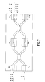
- the second embodiment is illustrated in the diagram in FIG. 4 which represents a wavelength converter comprising an interferometric structure of the Mach-Zehnder type in which the length of the active guides of the peripheral amplifiers for output OA 3 and input OA 4 and OA 5 is less than a determined limit value.
- the input saturation power of a semiconductor optical amplifier varies inversely with the length of the active guide of this amplifier. Consequently, to increase the saturation power of the peripheral amplifiers, and in particular that of the output amplifier OA 3 , the length of their active guide is restricted.
- the degradation of the extinction rate occurs essentially in the output amplifier OA 3 , after the coupler K 3 , but also at the output of the input amplifiers OA 4 and OA 5 , before the couplers K 2 and K 1 .
- This degradation of the extinction rate increases with the length of the active waveguide of these amplifiers because the associated saturation power decreases.
- the length of the active guide of a peripheral amplifier is defined as being the length L2 of the guide portion located at the ends of the converter, that is to say between a coupler K 3 or K 1 and the output or l entry of the interferometric structure.
- the length L1 of the first portion of the active guide, of the output amplifier OA 3 which is located before the junction Y, that is to say before the coupler K 3 , is less important.
- the converted signal AM 1 has not yet interfered with the signal AM 2 supplied by the second amplifier OA 2 of the interferometer and is still modulated in phase: the saturation of the amplifier OA 3 output therefore does not modify, in this guide portion, the signal extinction rate. Consequently, the length L1 of the guide portion preceding the coupler K 3 is not restricted.
- the saturation power of the output amplifier OA 3 becomes too weak to allow the interferometer to operate at a suitable output power Ps and with a signal to noise ratio S / B and an extinction rate TE not degraded.
- This limit value of the length L2 of the guide of the peripheral amplifier is equal to 300 ⁇ m.
- the curves of FIGS. 5A to 5C make it possible to compare the results obtained from a peripheral amplifier, for example the output amplifier OA 3 , in which the length L2 of the ribbon of active layer is respectively equal to and less than 300 ⁇ m.
- the overall length L of the compared amplifier remains identical. Indeed, in both cases, the sum of the length L2 of the guide portion located after the coupler K 3 and the length L1 of the guide portion located before this coupler is identical and equal, in the example illustrated on Figures 5A to 5C, at 600 ⁇ m.
- the degradation of the TE extinction rate is greater than 1 or even 2 dB when the length of the amplifier is 300 ⁇ m, while it remains strictly below 1dB when the length of the amplifier is 150 ⁇ m.
- the length of the active waveguide at least at least one peripheral amplifier is preferably less than 300 ⁇ m in order to increase the saturation threshold of this amplifier and maintain a rate of extinction optimum while maintaining an output power Ps suitable.
- the length of the active waveguide must however be both long enough to allow filtration high order optical modes and good quality of the interferometer, and short enough to avoid the effects of signal saturation. Through therefore, this length is preferably between 100 and 300 ⁇ m.
- FIG. 6 represents another structure of Michelson type equivalent to the previous one to which the invention applies.
- the two amplifiers OA 1 and OA 2 are coupled by only one of their ends, the opposite faces being provided with a reflective coating R1, R2.
- the modulating input signal E is injected into the first amplifier OA 1 via the face R1 and the output carrier wave M is injected into the two amplifiers OA 1 and OA 2 by the faces opposite to the faces R1 and R2, via a coupler K1 making it possible to couple one end of each of the branches 1 and 2 to a peripheral semiconductor optical amplifier OA 5 .
- An output signal S, of wavelength ⁇ S resulting from the coupling of auxiliary waves supplied by the first and second amplifiers OA 1 and OA 2 , is then amplified by the peripheral amplifier OA 5 .
- FIG. 7 represents another type of interferometric structure to which the invention applies.
- This type of structure concerns interferometric insertion-extraction multiplexers.
- the structure shown in Figure 7 corresponds to an "all active" device and includes peripheral amplifiers OA 7 , OA 8 , OA 9 , OA 10 at its ends.
- a multiplexed signal with 4 channels ABCD for example is injected into the amplifier referenced OA 7 .
- This signal is separated into two in branches 1 and 2 of the interferometer then recomposed and recovered at the output of the amplifier OA 9 .
- One of the signal channels, for example channel C can be suppressed by sending a control pulse by the amplifier OA 9 to phase-shift the pulses of the channel C in question.
- the signal recovered at the output of the amplifier OA 9 corresponds to the case referenced a) in FIG. 7 and now only includes 3 ABD channels. In the same way, one can then add another X channel by the amplifier OA 8 . In this case, referenced b) in FIG. 7, a multiplexed signal comprising 4 ABXD channels is recovered at the output of the amplifier OA 9 .
Abstract
Description
L'invention se rapporte à des systèmes optoélectroniques utilisés pour la transmission optique ou le traitement de données numériques optiques.The invention relates to systems optoelectronics used for optical transmission or the processing of optical digital data.
Elle se rapporte plus particulièrement à des structures interférométriques qui permettent de réaliser des convertisseurs de longueur d'onde et des multiplexeurs d'insertion-extraction utilisés dans le domaine des télécommunications. En particulier, les convertisseurs de longueur d'onde servent à convertir un signal optique transmis, d'une longueur d'onde à une autre longueur d'onde, tout en conservant ses performances.It relates more particularly to structures interferometric which allow to realize wavelength converters and multiplexers of insertion-extraction used in the field of telecommunications. In particular, the converters of wavelength are used to convert an optical signal transmitted, from one wavelength to another wavelength, while maintaining its performance.
De tels changements de longueur d'onde sont utilisés en particulier lors du routage des signaux pour résoudre les problèmes de contention.Such wavelength changes are used in especially when routing signals to resolve compression problems.
Dans ces dispositifs, les informations sont sous la forme de données binaires représentées par des impulsions modulant une onde porteuse optique. Une valeur binaire est donc déterminée en fonction du niveau d'amplitude (ou de puissance) de l'onde optique modulée.In these devices, the information is under the form of binary data represented by pulses modulating an optical carrier wave. A binary value is therefore determined according to the level of amplitude (or power) of the modulated optical wave.
Au cours de la transmission, ce signal peut subir des dégradations qui rendent plus difficile, au niveau des récepteurs, la détection des niveaux hauts et bas du signal reçu.During transmission, this signal may be subject to degradations that make it more difficult, in terms of receivers, detecting high and low signal levels received.
Dans le domaine de l'amplitude, la qualité d'un signal optique est habituellement définie par au moins deux paramètres : le rapport signal à bruit et le taux d'extinction.In the area of amplitude, the quality of a signal optics is usually defined by at least two parameters: signal-to-noise ratio and rate of extinction.
Le rapport signal à bruit est défini comme le rapport de la puissance optique du signal à la puissance du bruit dans une bande de longueur d'onde contenant la longueur d'onde de la porteuse du signal.The signal-to-noise ratio is defined as the ratio from optical signal power to noise power in a wavelength band containing the length wave of the signal carrier.
Le taux d'extinction est défini comme le rapport des puissances correspondant respectivement aux niveaux hauts et bas du signal. Ce taux doit être suffisamment élevé malgré les variations du signal d'entrée.The extinction rate is defined as the ratio of powers corresponding respectively to the high levels and signal down. This rate must be high enough despite variations in the input signal.
Une structure interférométrique est représentée sur la
figure 1 dans le cas du convertisseur de longueur d'onde.
Elle est constituée de deux branches guidantes 1 et 2. Au
moins une de ces branches est munie d'un amplificateur
optique semi-conducteur OA1. Cependant, en général on
préfère placer un deuxième amplificateur optique semi-conducteur
OA2 sur l'autre branche 2 pour des raisons de
symétrie. En effet, la présence du deuxième amplificateur
optique semi-conducteur OA2 permet de conserver sensiblement
le même niveau d'amplification dans les deux branches de la
structure et par conséquent d'avoir des puissances
sensiblement identiques en sortie des branches de
l'interféromètre.An interferometric structure is shown in Figure 1 in the case of the wavelength converter. It consists of two guiding
Ces deux amplificateurs optiques OA1, OA2 suffisent à former la structure interférométrique lorsque celle-ci est de type "actif-passif", c'est à dire lorsque les guides qui la composent sont réalisés à partir de deux types de matériaux, pour former des guides actifs et des guides passifs. Dans ce cas en effet, les guides situés aux extrémités de la structure interférométrique forment des guides passifs et sont réalisés dans un matériau non absorbant si bien que le signal optique en sortie de la structure interférométrique est identique au signal issu des amplificateurs OA1 et OA2. Cependant, la réalisation d'une telle structure intégrée de type "actif-passif" est très compliquée à mettre en oeuvre car elle nécessite plusieurs reprises d'épitaxie successives pour déposer les deux types de matériaux. La réalisation de cette structure étant longue et fastidieuse, son coût s'en trouve considérablement augmenté.These two optical amplifiers OA 1 , OA 2 are sufficient to form the interferometric structure when it is of the "active-passive" type, that is to say when the guides which compose it are produced from two types of material, for train active guides and passive guides. In this case, in fact, the guides located at the ends of the interferometric structure form passive guides and are made of a non-absorbent material so that the optical signal at the output of the interferometric structure is identical to the signal from the amplifiers OA 1 and OA 2 . However, the realization of such an integrated structure of the “active-passive” type is very complicated to implement because it requires several successive epitaxy recoveries to deposit the two types of material. The realization of this structure being long and tedious, its cost is considerably increased.
Pour simplifier la fabrication et diminuer le coût d'une telle structure interférométrique intégrée, on préfère donc réaliser une structure dite "toute active", c'est-à-dire une structure dont les guides sont tous actifs et formés dans un seul matériau. Cependant, dans ce cas le signal optique issu des amplificateurs OA1 et OA2 est fortement absorbé par le matériau utilisé et la puissance optique en sortie de la structure devient beaucoup trop faible pour être détectée. Par conséquent, dans une telle structure de type "tout actif", il est nécessaire de placer des amplificateurs optiques périphériques afin d'amplifier la puissance optique absorbée et de récupérer un signal convenable en sortie de la structure. Ces amplificateurs périphériques sont référencés OA3, OA4, OA5 et OA6 sur la figure 1.To simplify manufacture and reduce the cost of such an integrated interferometric structure, it is therefore preferable to produce a structure called "all active", that is to say a structure whose guides are all active and formed from a single material. However, in this case the optical signal from the amplifiers OA 1 and OA 2 is strongly absorbed by the material used and the optical power at the output of the structure becomes far too weak to be detected. Consequently, in such an “all active” type structure, it is necessary to place peripheral optical amplifiers in order to amplify the optical power absorbed and to recover a suitable signal at the output of the structure. These peripheral amplifiers are referenced OA 3 , OA 4 , OA 5 and OA 6 in Figure 1.
Les éléments constitutifs de la structure interférométrique de type "tout actif" représentée sur la figure 1 sont détaillés ci-dessous.The constituent elements of the structure "all active" interferometric type shown on the Figure 1 are detailed below.
Un premier coupleur K1 permet de coupler une extrémité de chacune de ces branches à un amplificateur optique semi-conducteur périphérique, encore dénommé amplificateur d'entrée OA5. Une source laser 7 permet par ailleurs de fournir, à cet amplificateur périphérique OA5, une onde porteuse de sortie M de longueur d'onde λS.A first coupler K 1 makes it possible to couple one end of each of these branches to a peripheral semiconductor optical amplifier, also called input amplifier OA 5 . A laser source 7 also makes it possible to supply, to this peripheral amplifier OA 5 , an output carrier wave M of wavelength λS.
Un second coupleur K2 est disposé de façon à coupler
l'autre extrémité de la première branche 1 à un autre
amplificateur optique semi-conducteur périphérique
d'entrée OA4. Ce coupleur K2 permet l'introduction, dans le
premier amplificateur OA1 d'un signal d'entrée E de longueur
d'onde λe ayant été amplifié par l'amplificateur
d'entrée OA4. L'amplificateur OA1 sature et l'état de
l'interféromètre est changé, ce qui entraíne une modulation
de phase de l'onde porteuse de sortie.A second coupler K 2 is arranged so as to couple the other end of the
Un troisième coupleur K3 relié au coupleur K2, au deuxième amplificateur OA2, et à un autre amplificateur optique semi-conducteur périphérique OA3, dit de sortie, est disposé de façon à fournir un signal de sortie S résultant du couplage d'ondes auxiliaires AM1 et AM2 fournies respectivement par les premier et deuxième amplificateurs OA1 et OA2. Les ondes AM1 et AM2 correspondent aux ondes M1 et M2 issues du coupleur K1 et amplifiées respectivement par les amplificateurs OA1 et OA2. Le signal de sortie S, de longueur d'onde λs, est ensuite amplifié par l'amplificateur périphérique de sortie OA3.A third coupler K 3 connected to the coupler K 2 , to the second amplifier OA 2 , and to another optical semiconductor optical amplifier OA 3 , called output, is arranged so as to supply an output signal S resulting from the coupling of auxiliary waves AM 1 and AM 2 supplied respectively by the first and second amplifiers OA 1 and OA 2 . The waves AM 1 and AM 2 correspond to the waves M 1 and M 2 coming from the coupler K 1 and amplified respectively by the amplifiers OA 1 and OA 2 . The output signal S, of wavelength λs, is then amplified by the peripheral output amplifier OA 3 .
Un autre amplificateur périphérique OA6 est par ailleurs prévu pour respecter la symétrie de la structure et pour permettre le remplacement de l'un des amplificateurs OA3 ou OA4 dans le cas d'une éventuelle panne.Another peripheral amplifier OA 6 is also provided to respect the symmetry of the structure and to allow the replacement of one of the amplifiers OA 3 or OA 4 in the event of a possible failure.
Des courants I1 et I2 sont injectés respectivement dans les amplificateurs OA1 et OA2, au travers d'électrodes E1 et E2. Le signal de sortie S résulte d'une interférence constructive ou destructrice des ondes AM1 et AM2, selon la différence de phase entre les deux branches de l'interféromètre.Currents I1 and I2 are injected respectively into the amplifiers OA 1 and OA 2 , through electrodes E1 and E2. The output signal S results from a constructive or destructive interference from the waves AM 1 and AM 2 , according to the phase difference between the two branches of the interferometer.
Pour assurer une conversion de longueur d'onde
efficace, le seuil de puissance de saturation des
amplificateurs OA1 et OA2 situés dans les branches 1 et 2
d'une telle structure interférométrique est fixé
relativement bas. Par conséquent, lorsque l'interférence des
ondes AM1 et AM2 est constructive, c'est à dire lorsque les
ondes AM1 et AM2 sont en phase, les puissances optiques des
deux amplificateurs OA1 et OA2 s'ajoutent si bien que la
puissance optique dans l'amplificateur de sortie OA3 est
très élevée.To ensure efficient wavelength conversion, the saturation power threshold of the amplifiers OA 1 and OA 2 located in the
Dans ce cas, l'amplificateur de sortie OA3 sature fortement et le taux d'extinction s'en trouve très dégradé. En effet, le gain des niveaux hauts devient inférieur au gain des niveaux bas, si bien que le signal de sortie S subit une compression des niveaux hauts et se trouve par conséquent déformé. Cette déformation peut également se produire sur le signal d'entrée E, ou sur l'onde porteuse de sortie M. Or, si le signal d'entrée E est déformé, ou si l'onde porteuse de sortie M est déformée, alors le signal de sortie S est également dégradé et le taux d'extinction de la structure interférométrique est amoindri. In this case, the output amplifier OA 3 strongly saturates and the extinction rate is very degraded. In fact, the gain of the high levels becomes lower than the gain of the low levels, so that the output signal S undergoes compression of the high levels and is consequently distorted. This deformation can also occur on the input signal E, or on the output carrier wave M. Or, if the input signal E is deformed, or if the output carrier wave M is deformed, then the output signal S is also degraded and the rate of extinction of the interferometric structure is reduced.
Il apparaít donc souhaitable que les amplificateurs périphériques puissent fonctionner en régime non saturé.It therefore appears desirable that the amplifiers devices can operate in unsaturated mode.
De manière générale, la puissance de saturation d'entrée d'un amplificateur est définie par la puissance optique d'entrée pour laquelle le gain de l'amplificateur est divisé par 2.Generally speaking, the saturation power input of an amplifier is defined by the power input optics for which the amplifier gain is divided by 2.
Les inconvénients précités peuvent apparaítre dans toute structure interférométrique "toute active". L'invention a pour but de remédier à ces inconvénients en proposant une structure qui, par rapport aux structures connues, rend la puissance de saturation d'entrée des amplificateurs périphériques plus difficile à atteindre par la puissance d'entrée de ces amplificateurs. Pour cela, on peut soit chercher à augmenter la puissance de saturation d'entrée desdits amplificateurs soit faire de telle sorte que la puissance d'entrée de ces amplificateurs soit réduite. Elle a plus précisément pour objet une structure interférométrique intégrée pour fournir un signal optique de sortie, dans laquelle une première et une seconde branche, comportant au moins un premier amplificateur optique semi-conducteur, sont couplées à des amplificateurs optiques semi-conducteurs périphériques d'entrée et/ou de sortie, caractérisée en ce que ladite structure comporte une section d'atténuation entre la sortie d'au moins un amplificateur optique semi-conducteur d'une des branches et l'entrée de l'amplificateur périphérique de sortie et/ou la longueur du guide d'onde d'au moins un amplificateur périphérique est inférieure à 300 µm.The aforementioned drawbacks may appear in any "all active" interferometric structure. The object of the invention is to remedy these drawbacks by proposing a structure which, compared to structures known, makes the input saturation power of peripheral amplifiers more difficult to reach by the input power of these amplifiers. For that, we can either seek to increase the saturation power input of said amplifiers either do so that the input power of these amplifiers is scaled down. More specifically, it has a structure interferometric integrated to provide an optical signal of output, in which a first and a second branch, comprising at least a first semiconductor optical amplifier, are coupled to optical amplifiers input and / or output peripheral semiconductors, characterized in that said structure has a section attenuation between the output of at least one amplifier semiconductor optics of one of the branches and the input of the peripheral output amplifier and / or the length of the waveguide of at least one peripheral amplifier is less than 300 µm.
Selon une autre caractéristique de l'invention, la section d'atténuation apporte au moins 50% de pertes optiques.According to another characteristic of the invention, the attenuation section brings at least 50% losses optical.
D'autres particularités et avantages de l'invention apparaítront à la lecture de la description donnée, dans le cas particulier du convertisseur de longueur, d'onde à titre d'exemple illustratif mais non limitatif, et faite en référence aux figures annexées qui représentent :
- la figure 1, déjà décrite, un schéma d'une structure interférométrique de type Mach-Zehnder connue à amplificateurs optiques semi-conducteurs périphériques,
- la figure 2, un schéma d'un convertisseur de longueur d'onde selon un premier mode de réalisation,
- les figures 3A à 3C, des courbes de variation, respectivement de la puissance de sortie (Ps), du taux d'extinction (TE) et du rapport signal à bruit (S/B) en fonction du courant (I) injecté et du taux de transmission optique dans un amplificateur périphérique,
- la figure 4, un schéma d'un convertisseur de longueur d'onde selon un autre mode de réalisation,
- les figures 5A à 5C, des courbes de variation, respectivement de la puissance de sortie (Ps), du taux d'extinction (TE) et du rapport signal à bruit (S/B) en fonction du courant (I) injecté et de la longueur du guide d'onde d'un amplificateur périphérique,
- la figure 6, un schéma d'une structure de type Michelson à laquelle s'applique l'invention,
- la figure 7, un schéma d'une structure de type multiplexeur interférométrique d'insertion-extraction.
- FIG. 1, already described, a diagram of an interferometric structure of the known Mach-Zehnder type with peripheral semiconductor optical amplifiers,
- FIG. 2, a diagram of a wavelength converter according to a first embodiment,
- FIGS. 3A to 3C, variation curves, respectively of the output power (Ps), the extinction rate (TE) and the signal to noise ratio (S / B) as a function of the current (I) injected and the optical transmission rate in a peripheral amplifier,
- FIG. 4, a diagram of a wavelength converter according to another embodiment,
- FIGS. 5A to 5C, variation curves, respectively of the output power (Ps), of the extinction rate (TE) and of the signal to noise ratio (S / B) as a function of the current (I) injected and of the length of the waveguide of a peripheral amplifier,
- FIG. 6, a diagram of a Michelson-type structure to which the invention applies,
- FIG. 7, a diagram of a structure of the interferometric insertion-extraction multiplexer type.
Dans tout le reste de la description, les mêmes références sont utilisées pour désigner les mêmes éléments.Throughout the rest of the description, the same references are used to designate the same elements.
Pour pouvoir effectuer des conversions de longueur d'onde efficaces, les amplificateurs optiques semi-conducteurs OA1 et OA2 situés sur les branches des interféromètres de type Mach-Zehnder ou équivalent doivent présenter un seuil de saturation relativement bas.In order to be able to carry out effective wavelength conversions, the optical semiconductor amplifiers OA 1 and OA 2 situated on the branches of the interferometers of the Mach-Zehnder type or equivalent must have a relatively low saturation threshold.
Au contraire, pour que le taux d'extinction soit optimum en sortie de l'interféromètre et pour éviter que le signal d'entrée E et l'onde porteuse de sortie M ne soient eux aussi déformés, il convient que les amplificateurs périphériques OA3, OA4 et OA5 fonctionnent en régime aussi peu saturé que possible. Pour cela, la structure doit être telle que le seuil de saturation d'entrée soit plus difficilement atteint par la puissance d'entrée. On the contrary, for the extinction rate to be optimum at the output of the interferometer and to prevent the input signal E and the output carrier wave M from also being distorted, the peripheral amplifiers OA 3 should be , OA 4 and OA 5 operate in the lowest saturation regime possible. For this, the structure must be such that the input saturation threshold is more difficult to reach by the input power.
Pour obtenir une telle structure, on peut soit réduire la puissance optique injectée dans cet amplificateur ou alors augmenter son seuil de saturation.To obtain such a structure, we can either reduce the optical power injected into this amplifier or then increase its saturation threshold.
Pour éviter une dégradation du taux d'extinction en sortie de l'interféromètre, on modifie les conditions de fonctionnement d'au moins un amplificateur périphérique. Ces conditions de fonctionnement sont notamment la puissance optique à l'entrée de l'amplificateur ou encore sa puissance de saturation d'entrée. De préférence, ce sont les conditions de fonctionnement de l'amplificateur de sortie qui sont prioritairement modifiées. Les conditions de fonctionnement des autres amplificateurs périphériques OA4 puis OA5 peuvent ensuite être modifiées pour éviter toute déformation du signal d'entrée E de l'onde porteuse de sortie M.To avoid degradation of the extinction rate at the output of the interferometer, the operating conditions of at least one peripheral amplifier are modified. These operating conditions include the optical power at the input of the amplifier or its input saturation power. Preferably, it is the operating conditions of the output amplifier that are first modified. The operating conditions of the other peripheral amplifiers OA 4 then OA 5 can then be modified to avoid any distortion of the input signal E of the output carrier wave M.
Un premier mode de réalisation d'un convertisseur de longueur d'onde selon l'invention consiste à permettre une réduction de la puissance optique injectée dans l'amplificateur périphérique de sortie OA3. Ce premier mode de réalisation est illustré sur le schéma de la figure 2 qui représente un convertisseur de longueur d'onde comportant une structure interférométrique de type Mach-Zehnder.A first embodiment of a wavelength converter according to the invention consists in enabling the optical power injected into the peripheral output amplifier OA 3 to be reduced. This first embodiment is illustrated in the diagram in FIG. 2 which represents a wavelength converter comprising an interferometric structure of the Mach-Zehnder type.
De manière avantageuse ce convertisseur comporte une
section d'atténuation 10, représentée en traits hachurés sur
la figure 2, située entre la sortie de l'amplificateur
optique OA1 de la première branche 1 et l'entrée de
l'amplificateur périphérique de sortie OA3.Advantageously, this converter includes an
De manière générale, la position de l'entrée de l'amplificateur de sortie OA3 est définie comme étant située juste derrière le coupleur K3 et non à la limite de l'électrode E3.In general, the position of the input of the output amplifier OA 3 is defined as being located just behind the coupler K 3 and not at the limit of the electrode E 3 .
La section d'atténuation 10 est obtenue en introduisant
des pertes optiques dans le bras correspondant 11 de guide
d'onde.The
Pour cela, le bras 11 de guide d'onde peut par exemple
être interrompu afin de diffracter une partie de la lumière.
Dans ce cas, le guide possède par exemple deux sections
effilées en regard l'une de l'autre, ce qui permet de
diffracter une partie de la puissance lumineuse et d'en
réinjecter une autre partie. Ce cas est le plus simple à
réaliser car seule la forme du masque utilisé pour réaliser
la gravure du guide d'onde change.For this, the
Une autre méthode pour introduire ces pertes consiste
par exemple à courber le bras 11 du guide, par rapport à
l'extrémité de l'amplificateur OA1, selon une pente plus
importante.Another method for introducing these losses consists, for example, in bending the
Les pertes peuvent également être introduites seulement au niveau du coupleur K3 en utilisant par exemple un coupleur mal adapté à la structure interférométrique.The losses can also be introduced only at the level of the coupler K 3 by using for example a coupler badly adapted to the interferometric structure.
Bien sûr ces méthodes ne sont que des exemples. En fait
toutes les méthodes connues qui permettent d'introduire des
pertes optiques dans la section 10 du convertisseur peuvent
être utilisées.Of course these methods are only examples. In fact
all known methods which allow the introduction of
optical losses in
Dans une variante de réalisation, la section
d'atténuation peut en outre être réalisée entre la sortie
des deux amplificateurs OA1, OA2 et l'entrée de
l'amplificateur de sortie OA3, le long des bras 11 et 12 de
guide d'onde.In an alternative embodiment, the attenuation section can also be produced between the output of the two amplifiers OA 1 , OA 2 and the input of the output amplifier OA 3 , along the
Les courbes des figures 3A à 3C permettent de comparer les résultats obtenus à partir d'un convertisseur de longueur d'onde comportant une section d'atténuation, entre les amplificateurs OA1 et OA2 et l'amplificateur OA3, apportant respectivement:
- aucune perte optique (Puissance optique totale dans
l'amplificateur OA3 Pt=200%=somme des puissances de sortie
des amplificateurs OA1 et OA2 ; et taux de transmission
optique de chaque
bras 11 et 12 t= 100%), - 80% de pertes optiques ( Puissance optique totale
Pt=120% et taux de transmission de chaque
bras 11 et 12 t=60%), et - 120% de pertes optiques (Puissance optique totale
Pt=80% et taux de transmission de chaque
bras 11 et 12 t=40%).
- no optical loss (Total optical power in the amplifier OA 3 Pt = 200% = sum of the output powers of the amplifiers OA 1 and OA 2 ; and optical transmission rate of each
arm 11 and 12 t = 100%), - 80% of optical losses (total optical power Pt = 120% and transmission rate of each
arm 11 and 12 t = 60%), and - 120% optical losses (Total optical power Pt = 80% and transmission rate of each
arm 11 and 12 t = 40%).
Le but à atteindre est d'obtenir un niveau de puissance de sortie Ps du convertisseur constant sans détériorer le taux d'extinction TE ni le rapport signal à bruit S/B.The goal is to get a power level Ps output from the constant converter without damaging the TE extinction rate or S / N signal-to-noise ratio.
Ces courbes indiquent que, pour une même puissance de
sortie Ps, le taux d'extinction TE augmente avec la
diminution de la transmission, c'est à dire avec
l'augmentation du coefficient d'atténuation dans les bras 11
et 12. Le rapport signal à bruit S/B, quant à lui, reste
sensiblement équivalent.These curves indicate that, for the same power of
output Ps, the TE extinction rate increases with the
decrease in transmission, i.e. with
increasing the attenuation coefficient in the
Par conséquent il est préférable d'atténuer fortement la puissance optique en sortie des amplificateurs OA1 et/ou OA2 pour maintenir un taux d'extinction optimum en sortie du convertisseur et éviter la déformation du signal. Ainsi, la structure de la section d'atténuation est telle qu'elle permet un apport d'au moins 50% de pertes optiques.Consequently, it is preferable to greatly attenuate the optical power at the output of the amplifiers OA 1 and / or OA 2 to maintain an optimum extinction rate at the output of the converter and to avoid distortion of the signal. Thus, the structure of the attenuation section is such that it allows a contribution of at least 50% of optical losses.
De préférence, la section d'atténuation 10 dans les
bras 11 et 12, située entre la sortie des l'amplificateurs
OA1 et OA2 respectivement et l'entrée de l'amplificateur de
sortie OA3, apporte au moins 50% de pertes optiques dans
chaque bras 11 et 12 pour permettre de réduire d'un facteur
2 la puissance optique totale dans le coupleur K3, c'est à
dire la puissance injectée dans l'amplificateur de sortie
OA3.Preferably, the
Un deuxième mode de réalisation d'un convertisseur de longueur d'onde selon l'invention consiste à augmenter le seuil de saturation d'au moins un amplificateur périphérique. Pour cela, la structure du guide d'onde actif de cet amplificateur périphérique est modifiée.A second embodiment of a converter wavelength according to the invention consists in increasing the saturation threshold of at least one amplifier peripheral. For this, the structure of the active waveguide of this peripheral amplifier is changed.
De préférence, c'est la structure du guide de l'amplificateur de sortie OA3 qui est prioritairement modifiée pour maintenir un bon taux d'extinction du signal de sortie S, et éviter ainsi toute déformation de ce signal. La structure des autres amplificateurs périphériques d'entrée OA4 puis OA5 peut ensuite être modifiée afin d'éviter toute déformation du signal d'entrée E et de l'onde porteuse de sortie M.Preferably, it is the structure of the guide of the output amplifier OA 3 which is priority modified to maintain a good rate of extinction of the output signal S, and thus to avoid any distortion of this signal. The structure of the other peripheral input amplifiers OA 4 then OA 5 can then be modified in order to avoid any distortion of the input signal E and of the output carrier wave M.
Le deuxième mode de réalisation est illustré sur le schéma de la figure 4 qui représente un convertisseur de longueur d'onde comportant une structure interférométrique de type Mach-Zehnder dans lequel la longueur des guides actifs des amplificateurs périphériques de sortie OA3 et d'entrée OA4 et OA5 est inférieure à une valeur limite déterminée.The second embodiment is illustrated in the diagram in FIG. 4 which represents a wavelength converter comprising an interferometric structure of the Mach-Zehnder type in which the length of the active guides of the peripheral amplifiers for output OA 3 and input OA 4 and OA 5 is less than a determined limit value.
La puissance de saturation d'entrée d'un amplificateur optique semi-conducteur varie inversement à la longueur du guide actif de cet amplificateur. Par conséquent, pour augmenter la puissance de saturation des amplificateurs périphériques, et notamment celle de l'amplificateur de sortie OA3, la longueur de leur guide actif est restreinte.The input saturation power of a semiconductor optical amplifier varies inversely with the length of the active guide of this amplifier. Consequently, to increase the saturation power of the peripheral amplifiers, and in particular that of the output amplifier OA 3 , the length of their active guide is restricted.
La dégradation du taux d'extinction se produit essentiellement dans l'amplificateur de sortie OA3, après le coupleur K3, mais aussi à la sortie des amplificateurs d'entrée OA4 et OA5, avant les coupleurs K2 et K1. Cette dégradation du taux d'extinction augmente avec la longueur du guide d'onde actif de ces amplificateurs car la puissance de saturation associée diminue.The degradation of the extinction rate occurs essentially in the output amplifier OA 3 , after the coupler K 3 , but also at the output of the input amplifiers OA 4 and OA 5 , before the couplers K 2 and K 1 . This degradation of the extinction rate increases with the length of the active waveguide of these amplifiers because the associated saturation power decreases.
De manière générale, on définit la longueur du guide actif d'un amplificateur périphérique comme étant la longueur L2 de la portion de guide située aux extrémités du convertisseur, c'est à dire entre un coupleur K3 ou K1 et la sortie ou l'entrée de la structure interférométrique.In general, the length of the active guide of a peripheral amplifier is defined as being the length L2 of the guide portion located at the ends of the converter, that is to say between a coupler K 3 or K 1 and the output or l entry of the interferometric structure.
La longueur L1 de la première portion du guide actif, de l'amplificateur de sortie OA3, qui est située avant la jonction Y, c'est à dire avant le coupleur K3, est moins importante. En effet, dans cette portion de guide, le signal converti AM1 n'a pas encore interféré avec le signal AM2 fournit par le deuxième amplificateur OA2 de l'interféromètre et est encore modulé en phase : la saturation de l'amplificateur de sortie OA3 ne modifie donc pas, dans cette portion de guide, le taux d'extinction du signal. Par conséquent la longueur L1 de la portion de guide précédant le coupleur K3 n'est pas restreinte.The length L1 of the first portion of the active guide, of the output amplifier OA 3 , which is located before the junction Y, that is to say before the coupler K 3 , is less important. In fact, in this portion of the guide, the converted signal AM 1 has not yet interfered with the signal AM 2 supplied by the second amplifier OA 2 of the interferometer and is still modulated in phase: the saturation of the amplifier OA 3 output therefore does not modify, in this guide portion, the signal extinction rate. Consequently, the length L1 of the guide portion preceding the coupler K 3 is not restricted.
En revanche, si la longueur à prendre effectivement en compte, c'est à dire la longueur L2 de la deuxième portion du guide actif située après le coupleur K3, est supérieure à une valeur limite déterminée, alors la puissance de saturation de l'amplificateur de sortie OA3 devient trop faible pour permettre à l'interféromètre de fonctionner à une puissance de sortie Ps convenable et avec un rapport signal à bruit S/B et un taux d'extinction TE non dégradés. Cette valeur limite de la longueur L2 du guide de l'amplificateur périphérique est égale à 300 µm.On the other hand, if the length to be effectively taken into account, ie the length L2 of the second portion of the active guide located after the coupler K 3 , is greater than a determined limit value, then the saturation power of the output amplifier OA 3 becomes too weak to allow the interferometer to operate at a suitable output power Ps and with a signal to noise ratio S / B and an extinction rate TE not degraded. This limit value of the length L2 of the guide of the peripheral amplifier is equal to 300 μm.
Les courbes des figures 5A à 5C permettent de comparer les résultats obtenus à partir d'un amplificateur périphérique, par exemple l'amplificateur de sortie OA3, dans lequel la longueur L2 du ruban de couche active est respectivement égale et inférieure à 300 µm.The curves of FIGS. 5A to 5C make it possible to compare the results obtained from a peripheral amplifier, for example the output amplifier OA 3 , in which the length L2 of the ribbon of active layer is respectively equal to and less than 300 μm.
Cependant, dans les deux cas, la longueur globale L de l'amplificateur comparé reste identique. En effet, dans les deux cas, la somme de la longueur L2 de la portion de guide située après le coupleur K3 et de la longueur L1 de la portion de guide située avant ce coupleur est identique et égale, dans l'exemple illustré sur les figures 5A à 5C, à 600 µm.However, in both cases, the overall length L of the compared amplifier remains identical. Indeed, in both cases, the sum of the length L2 of the guide portion located after the coupler K 3 and the length L1 of the guide portion located before this coupler is identical and equal, in the example illustrated on Figures 5A to 5C, at 600 µm.
Ces courbes indiquent que, pour une même puissance de sortie Ps et pour un rapport signal à bruit S/B équivalent, on obtient une dégradation du taux d'extinction beaucoup plus faible lorsque la longueur du guide est inférieure à 300 µm.These curves indicate that, for the same power of Ps output and for an equivalent S / N signal to noise ratio, we get a degradation of the extinction rate a lot lower when the guide length is less than 300 µm.
Ainsi, pour une puissance de sortie supérieure à -5 dBm, la dégradation du taux d'extinction TE est supérieure à 1 voire 2 dB lorsque la longueur de l'amplificateur est de 300µm, alors qu'elle reste strictement inférieure à 1dB lorsque la longueur de l'amplificateur est égale à 150 µm. Thus, for an output power greater than -5 dBm, the degradation of the TE extinction rate is greater than 1 or even 2 dB when the length of the amplifier is 300µm, while it remains strictly below 1dB when the length of the amplifier is 150 µm.
Par conséquent, la longueur du guide d'onde actif d'au moins un amplificateur périphérique est de préférence inférieure à 300µm afin d'augmenter le seuil de saturation de cet amplificateur et de maintenir un taux d'extinction optimum tout en conservant une puissance de sortie Ps convenable.Therefore, the length of the active waveguide at least at least one peripheral amplifier is preferably less than 300µm in order to increase the saturation threshold of this amplifier and maintain a rate of extinction optimum while maintaining an output power Ps suitable.
La longueur du guide d'onde actif doit cependant être à la fois suffisamment longue pour permettre une filtration des modes optiques d'ordres élevés et un fonctionnement de bonne qualité de l'interféromètre, et suffisamment courte pour éviter les effets de saturation du signal. Par conséquent, cette longueur est de préférence comprise entre 100 et 300µm.The length of the active waveguide must however be both long enough to allow filtration high order optical modes and good quality of the interferometer, and short enough to avoid the effects of signal saturation. Through therefore, this length is preferably between 100 and 300µm.
Les modes de réalisation qui viennent d'être décrits sont très simples à mettre en oeuvre puisqu'ils ne nécessitent pas d'étape de technologie supplémentaire au cours de la fabrication des composants optiques. Dans la réalisation la plus simple, seule la forme du masque utilisé pour réaliser la gravure des guides d'onde actifs change.The embodiments which have just been described are very simple to implement since they do not require no additional technology step at during the manufacturing of optical components. In the simplest realization, only the shape of the mask used to engrave the active waveguides changes.
La figure 6 représente une autre structure de type
Michelson équivalente à la précédente à laquelle s'applique
l'invention. Selon cette variante, les deux amplificateurs
OA1 et OA2 sont couplés par une seule de leurs extrémités,
les faces opposées étant munies d'un revêtement
réfléchissant R1, R2. Le signal d'entrée modulant E est
injecté dans le premier amplificateur OA1 par
l'intermédiaire de la face R1 et l'onde porteuse de sortie M
est injectée dans les deux amplificateurs OA1 et OA2 par les
faces opposées aux faces R1 et R2, par l'intermédiaire d'un
coupleur K1 permettant de coupler une extrémité de chacune
des branches 1 et 2 à un amplificateur optique semi-conducteur
périphérique OA5. Un signal de sortie S, de
longueur d'onde λS, résultant du couplage d'ondes
auxiliaires fournies par les premier et deuxième
amplificateurs OA1 et OA2, est ensuite amplifié par
l'amplificateur périphérique OA5. FIG. 6 represents another structure of Michelson type equivalent to the previous one to which the invention applies. According to this variant, the two amplifiers OA 1 and OA 2 are coupled by only one of their ends, the opposite faces being provided with a reflective coating R1, R2. The modulating input signal E is injected into the first amplifier OA 1 via the face R1 and the output carrier wave M is injected into the two amplifiers OA 1 and OA 2 by the faces opposite to the faces R1 and R2, via a coupler K1 making it possible to couple one end of each of the
La figure 7 représente un autre type de structure
interférométrique à laquelle s'applique l'invention. Ce type
de structure concerne les multiplexeurs interférométriques
d'insertion-extraction. La structure représentée sur la
figure 7 correspond à un dispositif "tout actif" et comprend
des amplificateurs périphériques OA7, OA8, OA9, OA10 à ses
extrémités. Un signal multiplexé à 4 canaux ABCD par exemple
est injecté dans l'amplificateur référencé OA7. Ce signal
est séparé en deux dans les branches 1 et 2 de
l'interféromètre puis recomposé et récupéré à la sortie de
l'amplificateur OA9. L'un des canaux du signal, par exemple
le canal C, peut être supprimé en envoyant une impulsion de
contrôle par l'amplificateur OA9 pour déphaser les
impulsions du canal C en question. Le signal récupéré à la
sortie de l'amplificateur OA9 correspond alors au cas
référencé a) sur la figure 7 et ne comprend plus que 3
canaux ABD. De la même façon, on peut ensuite ajouter un
autre canal X par l'amplificateur OA8. Dans ce cas,
référencé b) sur la figure 7, on récupère à la sortie de
l'amplificateur OA9 un signal multiplexé comprenant 4 canaux
ABXD.FIG. 7 represents another type of interferometric structure to which the invention applies. This type of structure concerns interferometric insertion-extraction multiplexers. The structure shown in Figure 7 corresponds to an "all active" device and includes peripheral amplifiers OA 7 , OA 8 , OA 9 , OA 10 at its ends. A multiplexed signal with 4 channels ABCD for example is injected into the amplifier referenced OA 7 . This signal is separated into two in
Claims (5)
Applications Claiming Priority (3)
| Application Number | Priority Date | Filing Date | Title |
|---|---|---|---|
| FR9711122 | 1997-09-08 | ||
| FR9711122A FR2768231B1 (en) | 1997-09-08 | 1997-09-08 | INTEGRATED INTERFEROMETRIC STRUCTURE |
| US09/148,187 US6035078A (en) | 1997-09-08 | 1998-09-04 | Integrated interferometer structure |
Publications (2)
| Publication Number | Publication Date |
|---|---|
| EP0902512A2 true EP0902512A2 (en) | 1999-03-17 |
| EP0902512A3 EP0902512A3 (en) | 1999-05-19 |
Family
ID=26233791
Family Applications (1)
| Application Number | Title | Priority Date | Filing Date |
|---|---|---|---|
| EP98402199A Withdrawn EP0902512A3 (en) | 1997-09-08 | 1998-09-07 | Integrated interferometric structure |
Country Status (5)
| Country | Link |
|---|---|
| US (1) | US6035078A (en) |
| EP (1) | EP0902512A3 (en) |
| JP (1) | JPH11142902A (en) |
| CA (1) | CA2243858A1 (en) |
| FR (1) | FR2768231B1 (en) |
Families Citing this family (12)
| Publication number | Priority date | Publication date | Assignee | Title |
|---|---|---|---|---|
| FR2781322B1 (en) * | 1998-07-20 | 2000-09-08 | Alsthom Cge Alcatel | OPTICAL DATA TRANSMISSION DEVICE |
| FR2786279B1 (en) * | 1998-11-24 | 2000-12-29 | Cit Alcatel | OPTICAL COMPONENT BASED ON SEMICONDUCTOR OPTICAL AMPLIFIERS WITH A REDUCED NUMBER OF INDEPENDENT ELECTRODES |
| JP2001147409A (en) | 1999-11-19 | 2001-05-29 | Ddi Corp | Optical signal processor |
| GB0007549D0 (en) * | 2000-03-28 | 2000-05-17 | Iltron Limited | A wavelength converter |
| US6563621B2 (en) * | 2000-10-06 | 2003-05-13 | Alphion Corporation | Bit-rate and format insensitive all-optical clock extraction circuit |
| US6570697B2 (en) * | 2000-10-06 | 2003-05-27 | Alphion Corporation | Format insensitive and bit rate independent optical preprocessor |
| US6646773B2 (en) | 2001-05-23 | 2003-11-11 | Board Of Regents, The University Of Texas System | Digital micro-mirror holographic projection |
| US20030068114A1 (en) * | 2001-08-02 | 2003-04-10 | Gayle Link | Semiconductor waveguide optical regenerative device |
| US6856751B2 (en) * | 2002-03-22 | 2005-02-15 | Lynx Photonic Networks, Inc. | Method and system for obtaining variable optical attenuation with very low polarization dependent loss over an ultra wide dynamic range |
| US6879738B2 (en) * | 2003-02-24 | 2005-04-12 | Intel Corporation | Method and apparatus for modulating an optical beam in an optical device |
| US7688502B2 (en) * | 2004-07-30 | 2010-03-30 | Yoshinobu Maeda | Three-terminal optical signal amplifying device |
| US6992813B1 (en) * | 2004-12-28 | 2006-01-31 | Fujitsu Limited | Optical amplifying device |
Citations (3)
| Publication number | Priority date | Publication date | Assignee | Title |
|---|---|---|---|---|
| JPH0519311A (en) * | 1991-07-16 | 1993-01-29 | Fujitsu Ltd | Optical amplification system |
| JPH05259581A (en) * | 1992-03-16 | 1993-10-08 | Nippon Telegr & Teleph Corp <Ntt> | Wavelength converter |
| EP0717482A1 (en) * | 1994-12-14 | 1996-06-19 | AT&T Corp. | Semiconductor interferometric optical wavelength conversion device |
Family Cites Families (6)
| Publication number | Priority date | Publication date | Assignee | Title |
|---|---|---|---|---|
| JPH0718964B2 (en) * | 1987-06-29 | 1995-03-06 | 日本電信電話株式会社 | Integrated optical device and manufacturing method thereof |
| US5233453A (en) * | 1992-04-29 | 1993-08-03 | International Business Machines Corporation | Space-division switched waveguide array filter and method using same |
| US5287376A (en) * | 1992-12-14 | 1994-02-15 | Xerox Corporation | Independently addressable semiconductor diode lasers with integral lowloss passive waveguides |
| DE19503929A1 (en) * | 1995-02-07 | 1996-08-08 | Ldt Gmbh & Co | Color imaging systems |
| US5703975A (en) * | 1995-06-09 | 1997-12-30 | Corning Incorporated | Interferometric switch |
| JP2765545B2 (en) * | 1995-12-26 | 1998-06-18 | 日本電気株式会社 | Optical wavelength discriminating circuit and method of manufacturing the same |
-
1997
- 1997-09-08 FR FR9711122A patent/FR2768231B1/en not_active Expired - Fee Related
-
1998
- 1998-09-04 US US09/148,187 patent/US6035078A/en not_active Expired - Lifetime
- 1998-09-04 CA CA002243858A patent/CA2243858A1/en not_active Abandoned
- 1998-09-07 JP JP10253078A patent/JPH11142902A/en active Pending
- 1998-09-07 EP EP98402199A patent/EP0902512A3/en not_active Withdrawn
Patent Citations (3)
| Publication number | Priority date | Publication date | Assignee | Title |
|---|---|---|---|---|
| JPH0519311A (en) * | 1991-07-16 | 1993-01-29 | Fujitsu Ltd | Optical amplification system |
| JPH05259581A (en) * | 1992-03-16 | 1993-10-08 | Nippon Telegr & Teleph Corp <Ntt> | Wavelength converter |
| EP0717482A1 (en) * | 1994-12-14 | 1996-06-19 | AT&T Corp. | Semiconductor interferometric optical wavelength conversion device |
Non-Patent Citations (4)
| Title |
|---|
| PATENT ABSTRACTS OF JAPAN vol. 017, no. 290 (P-1549), 3 juin 1993 & JP 05 019311 A (FUJITSU LTD), 29 janvier 1993 * |
| PATENT ABSTRACTS OF JAPAN vol. 018, no. 022 (E-1490), 13 janvier 1994 & JP 05 259581 A (NIPPON TELEGR & TELEPH CORP), 8 octobre 1993 * |
| S.L. DANIELSEN ET AL: "Compensation of gain saturation in SOA gates by interferometric Mach Zehnder wavelngth converters" PROCEEDINGS OF THE ECOC 1996, 22ND CONFERENC ON OPTICAL COMMUNICATION, vol. 4, 15 septembre 1996, pages 45-48, XP002066498 OSLO * |
| SCHILLING M ET AL: "WAVELENGHT CONVERTER BASED ON INTEGRATED ALL-ACTIVE THREE-PORT MACH-ZEHNDER INTERFEROMETER" ELECTRONICS LETTERS, vol. 30, no. 25, 8 décembre 1994, pages 2128-2130, XP000502092 * |
Also Published As
| Publication number | Publication date |
|---|---|
| JPH11142902A (en) | 1999-05-28 |
| FR2768231A1 (en) | 1999-03-12 |
| EP0902512A3 (en) | 1999-05-19 |
| FR2768231B1 (en) | 1999-12-10 |
| US6035078A (en) | 2000-03-07 |
| CA2243858A1 (en) | 1999-03-08 |
Similar Documents
| Publication | Publication Date | Title |
|---|---|---|
| EP0813097B1 (en) | Digital optical signal regeneration device and its use for modifying digital optical signals | |
| EP0902512A2 (en) | Integrated interferometric structure | |
| FR2685835A1 (en) | VERY LONG DISTANCE TRANSMISSION SYSTEM ON OPTICAL FIBER COMPENSATED FOR DISTORTIONS AT RECEPTION. | |
| EP1005120A1 (en) | Optical semiconductor device with a mode converter | |
| FR2695212A1 (en) | Optical filter device | |
| FR2933207A1 (en) | OPTICAL MODULATION DEVICE AND OPTICAL SEMICONDUCTOR DEVICE. | |
| FR2740620A1 (en) | OPTICAL AMPLIFIER, AND TOOL COMPRISING THE SAME | |
| EP0859268A1 (en) | Wavelength converter of binary optical signals | |
| FR2707442A1 (en) | Optical fiber transmission system with on-line distortion compensation. | |
| EP0871061A1 (en) | Wavelength converter of optical binary signals | |
| EP0881790B1 (en) | Optical transmission system with dynamic compensation of the transmitted power | |
| FR2695761A1 (en) | Method for manufacturing electro-optical ribbon devices, in particular lasers, and devices thus obtained. | |
| JP2002520821A (en) | Optical power measurement in photonic integrated devices | |
| FR2753285A1 (en) | SEMICONDUCTOR OPTICAL AMPLIFIER | |
| FR2785730A1 (en) | SEMICONDUCTOR OPTICAL AMPLIFIER WITH ADJUSTABLE STABILIZED GAIN AND OPTICAL SYSTEM USING SUCH AMPLIFIER | |
| FR2768232A1 (en) | METHOD FOR MANUFACTURING AN INTEGRATED OPTICAL COMPONENT COMPRISING A THICK WAVEGUIDE COUPLED TO A THIN WAVEGUIDE | |
| EP0562925A1 (en) | Semi-conductor waveguide photoreceiver with multiple quantum wells for polarisation diversity communications systems | |
| FR2801686A1 (en) | Optical network system signal processor having two optical paths with modulator/fixed phase relationship with combiner input and second signal input/combiner | |
| EP0783212A1 (en) | Optical signal distribution system | |
| EP1134859B1 (en) | Optical amplifying device | |
| CA2290142A1 (en) | Optical component based on semiconductor optical amplifiers containing a reduced number of separate electrodes | |
| EP3994509A1 (en) | Assembly of an active semiconductor component and of a passive silicon-based optical component | |
| EP1111819B1 (en) | Fiber optic transmission system with noise reduction using a non linear offset of the signals | |
| FR2746192A1 (en) | NON-LINEAR OPTICAL DEVICE FOR PROCESSING OPTICAL SIGNALS | |
| WO2024002925A1 (en) | Method and device for optical finite impulse response filtering and corresponding optical equipment |
Legal Events
| Date | Code | Title | Description |
|---|---|---|---|
| PUAI | Public reference made under article 153(3) epc to a published international application that has entered the european phase |
Free format text: ORIGINAL CODE: 0009012 |
|
| AK | Designated contracting states |
Kind code of ref document: A2 Designated state(s): DE ES GB IT SE |
|
| AX | Request for extension of the european patent |
Free format text: AL;LT;LV;MK;RO;SI |
|
| RAP3 | Party data changed (applicant data changed or rights of an application transferred) |
Owner name: ALCATEL |
|
| PUAL | Search report despatched |
Free format text: ORIGINAL CODE: 0009013 |
|
| AK | Designated contracting states |
Kind code of ref document: A3 Designated state(s): AT BE CH CY DE DK ES FI FR GB GR IE IT LI LU MC NL PT SE |
|
| AX | Request for extension of the european patent |
Free format text: AL;LT;LV;MK;RO;SI |
|
| 17P | Request for examination filed |
Effective date: 19991119 |
|
| AKX | Designation fees paid |
Free format text: DE ES GB IT SE |
|
| 17Q | First examination report despatched |
Effective date: 20030724 |
|
| RAP1 | Party data changed (applicant data changed or rights of an application transferred) |
Owner name: AVANEX CORPORATION |
|
| STAA | Information on the status of an ep patent application or granted ep patent |
Free format text: STATUS: THE APPLICATION IS DEEMED TO BE WITHDRAWN |
|
| 18D | Application deemed to be withdrawn |
Effective date: 20040204 |