EP0901154A2 - Méthode et système de fixation d'un dispositif semiconducteur, système de séparation de dispositifs semiconducteurs, et méthode de fabrication d'une carte IC - Google Patents
Méthode et système de fixation d'un dispositif semiconducteur, système de séparation de dispositifs semiconducteurs, et méthode de fabrication d'une carte IC Download PDFInfo
- Publication number
- EP0901154A2 EP0901154A2 EP98307158A EP98307158A EP0901154A2 EP 0901154 A2 EP0901154 A2 EP 0901154A2 EP 98307158 A EP98307158 A EP 98307158A EP 98307158 A EP98307158 A EP 98307158A EP 0901154 A2 EP0901154 A2 EP 0901154A2
- Authority
- EP
- European Patent Office
- Prior art keywords
- adhesive sheet
- semiconductor devices
- mounting
- group
- semiconductor device
- Prior art date
- Legal status (The legal status is an assumption and is not a legal conclusion. Google has not performed a legal analysis and makes no representation as to the accuracy of the status listed.)
- Withdrawn
Links
Images


Classifications
-
- H—ELECTRICITY
- H01—ELECTRIC ELEMENTS
- H01L—SEMICONDUCTOR DEVICES NOT COVERED BY CLASS H10
- H01L23/00—Details of semiconductor or other solid state devices
- H01L23/58—Structural electrical arrangements for semiconductor devices not otherwise provided for, e.g. in combination with batteries
- H01L23/64—Impedance arrangements
- H01L23/642—Capacitive arrangements
-
- H—ELECTRICITY
- H01—ELECTRIC ELEMENTS
- H01L—SEMICONDUCTOR DEVICES NOT COVERED BY CLASS H10
- H01L21/00—Processes or apparatus adapted for the manufacture or treatment of semiconductor or solid state devices or of parts thereof
- H01L21/02—Manufacture or treatment of semiconductor devices or of parts thereof
- H01L21/04—Manufacture or treatment of semiconductor devices or of parts thereof the devices having at least one potential-jump barrier or surface barrier, e.g. PN junction, depletion layer or carrier concentration layer
- H01L21/50—Assembly of semiconductor devices using processes or apparatus not provided for in a single one of the subgroups H01L21/06 - H01L21/326, e.g. sealing of a cap to a base of a container
-
- H—ELECTRICITY
- H01—ELECTRIC ELEMENTS
- H01L—SEMICONDUCTOR DEVICES NOT COVERED BY CLASS H10
- H01L21/00—Processes or apparatus adapted for the manufacture or treatment of semiconductor or solid state devices or of parts thereof
- H01L21/67—Apparatus specially adapted for handling semiconductor or electric solid state devices during manufacture or treatment thereof; Apparatus specially adapted for handling wafers during manufacture or treatment of semiconductor or electric solid state devices or components ; Apparatus not specifically provided for elsewhere
- H01L21/67005—Apparatus not specifically provided for elsewhere
- H01L21/67011—Apparatus for manufacture or treatment
- H01L21/67144—Apparatus for mounting on conductive members, e.g. leadframes or conductors on insulating substrates
-
- H—ELECTRICITY
- H01—ELECTRIC ELEMENTS
- H01L—SEMICONDUCTOR DEVICES NOT COVERED BY CLASS H10
- H01L21/00—Processes or apparatus adapted for the manufacture or treatment of semiconductor or solid state devices or of parts thereof
- H01L21/67—Apparatus specially adapted for handling semiconductor or electric solid state devices during manufacture or treatment thereof; Apparatus specially adapted for handling wafers during manufacture or treatment of semiconductor or electric solid state devices or components ; Apparatus not specifically provided for elsewhere
- H01L21/683—Apparatus specially adapted for handling semiconductor or electric solid state devices during manufacture or treatment thereof; Apparatus specially adapted for handling wafers during manufacture or treatment of semiconductor or electric solid state devices or components ; Apparatus not specifically provided for elsewhere for supporting or gripping
- H01L21/6835—Apparatus specially adapted for handling semiconductor or electric solid state devices during manufacture or treatment thereof; Apparatus specially adapted for handling wafers during manufacture or treatment of semiconductor or electric solid state devices or components ; Apparatus not specifically provided for elsewhere for supporting or gripping using temporarily an auxiliary support
- H01L21/6836—Wafer tapes, e.g. grinding or dicing support tapes
-
- H—ELECTRICITY
- H01—ELECTRIC ELEMENTS
- H01L—SEMICONDUCTOR DEVICES NOT COVERED BY CLASS H10
- H01L2221/00—Processes or apparatus adapted for the manufacture or treatment of semiconductor or solid state devices or of parts thereof covered by H01L21/00
- H01L2221/67—Apparatus for handling semiconductor or electric solid state devices during manufacture or treatment thereof; Apparatus for handling wafers during manufacture or treatment of semiconductor or electric solid state devices or components; Apparatus not specifically provided for elsewhere
- H01L2221/683—Apparatus for handling semiconductor or electric solid state devices during manufacture or treatment thereof; Apparatus for handling wafers during manufacture or treatment of semiconductor or electric solid state devices or components; Apparatus not specifically provided for elsewhere for supporting or gripping
- H01L2221/68304—Apparatus for handling semiconductor or electric solid state devices during manufacture or treatment thereof; Apparatus for handling wafers during manufacture or treatment of semiconductor or electric solid state devices or components; Apparatus not specifically provided for elsewhere for supporting or gripping using temporarily an auxiliary support
- H01L2221/68327—Apparatus for handling semiconductor or electric solid state devices during manufacture or treatment thereof; Apparatus for handling wafers during manufacture or treatment of semiconductor or electric solid state devices or components; Apparatus not specifically provided for elsewhere for supporting or gripping using temporarily an auxiliary support used during dicing or grinding
-
- H—ELECTRICITY
- H01—ELECTRIC ELEMENTS
- H01L—SEMICONDUCTOR DEVICES NOT COVERED BY CLASS H10
- H01L2221/00—Processes or apparatus adapted for the manufacture or treatment of semiconductor or solid state devices or of parts thereof covered by H01L21/00
- H01L2221/67—Apparatus for handling semiconductor or electric solid state devices during manufacture or treatment thereof; Apparatus for handling wafers during manufacture or treatment of semiconductor or electric solid state devices or components; Apparatus not specifically provided for elsewhere
- H01L2221/683—Apparatus for handling semiconductor or electric solid state devices during manufacture or treatment thereof; Apparatus for handling wafers during manufacture or treatment of semiconductor or electric solid state devices or components; Apparatus not specifically provided for elsewhere for supporting or gripping
- H01L2221/68304—Apparatus for handling semiconductor or electric solid state devices during manufacture or treatment thereof; Apparatus for handling wafers during manufacture or treatment of semiconductor or electric solid state devices or components; Apparatus not specifically provided for elsewhere for supporting or gripping using temporarily an auxiliary support
- H01L2221/68381—Details of chemical or physical process used for separating the auxiliary support from a device or wafer
- H01L2221/68386—Separation by peeling
- H01L2221/6839—Separation by peeling using peeling wedge or knife or bar
-
- H—ELECTRICITY
- H01—ELECTRIC ELEMENTS
- H01L—SEMICONDUCTOR DEVICES NOT COVERED BY CLASS H10
- H01L2221/00—Processes or apparatus adapted for the manufacture or treatment of semiconductor or solid state devices or of parts thereof covered by H01L21/00
- H01L2221/67—Apparatus for handling semiconductor or electric solid state devices during manufacture or treatment thereof; Apparatus for handling wafers during manufacture or treatment of semiconductor or electric solid state devices or components; Apparatus not specifically provided for elsewhere
- H01L2221/683—Apparatus for handling semiconductor or electric solid state devices during manufacture or treatment thereof; Apparatus for handling wafers during manufacture or treatment of semiconductor or electric solid state devices or components; Apparatus not specifically provided for elsewhere for supporting or gripping
- H01L2221/68304—Apparatus for handling semiconductor or electric solid state devices during manufacture or treatment thereof; Apparatus for handling wafers during manufacture or treatment of semiconductor or electric solid state devices or components; Apparatus not specifically provided for elsewhere for supporting or gripping using temporarily an auxiliary support
- H01L2221/68381—Details of chemical or physical process used for separating the auxiliary support from a device or wafer
- H01L2221/68386—Separation by peeling
- H01L2221/68395—Separation by peeling using peeling wheel
-
- H—ELECTRICITY
- H01—ELECTRIC ELEMENTS
- H01L—SEMICONDUCTOR DEVICES NOT COVERED BY CLASS H10
- H01L2224/00—Indexing scheme for arrangements for connecting or disconnecting semiconductor or solid-state bodies and methods related thereto as covered by H01L24/00
- H01L2224/01—Means for bonding being attached to, or being formed on, the surface to be connected, e.g. chip-to-package, die-attach, "first-level" interconnects; Manufacturing methods related thereto
- H01L2224/10—Bump connectors; Manufacturing methods related thereto
- H01L2224/15—Structure, shape, material or disposition of the bump connectors after the connecting process
- H01L2224/16—Structure, shape, material or disposition of the bump connectors after the connecting process of an individual bump connector
-
- H—ELECTRICITY
- H01—ELECTRIC ELEMENTS
- H01L—SEMICONDUCTOR DEVICES NOT COVERED BY CLASS H10
- H01L2924/00—Indexing scheme for arrangements or methods for connecting or disconnecting semiconductor or solid-state bodies as covered by H01L24/00
- H01L2924/01—Chemical elements
- H01L2924/01078—Platinum [Pt]
-
- H—ELECTRICITY
- H01—ELECTRIC ELEMENTS
- H01L—SEMICONDUCTOR DEVICES NOT COVERED BY CLASS H10
- H01L2924/00—Indexing scheme for arrangements or methods for connecting or disconnecting semiconductor or solid-state bodies as covered by H01L24/00
- H01L2924/01—Chemical elements
- H01L2924/01079—Gold [Au]
-
- H—ELECTRICITY
- H01—ELECTRIC ELEMENTS
- H01L—SEMICONDUCTOR DEVICES NOT COVERED BY CLASS H10
- H01L2924/00—Indexing scheme for arrangements or methods for connecting or disconnecting semiconductor or solid-state bodies as covered by H01L24/00
- H01L2924/06—Polymers
- H01L2924/078—Adhesive characteristics other than chemical
- H01L2924/0781—Adhesive characteristics other than chemical being an ohmic electrical conductor
- H01L2924/07811—Extrinsic, i.e. with electrical conductive fillers
-
- Y—GENERAL TAGGING OF NEW TECHNOLOGICAL DEVELOPMENTS; GENERAL TAGGING OF CROSS-SECTIONAL TECHNOLOGIES SPANNING OVER SEVERAL SECTIONS OF THE IPC; TECHNICAL SUBJECTS COVERED BY FORMER USPC CROSS-REFERENCE ART COLLECTIONS [XRACs] AND DIGESTS
- Y10—TECHNICAL SUBJECTS COVERED BY FORMER USPC
- Y10S—TECHNICAL SUBJECTS COVERED BY FORMER USPC CROSS-REFERENCE ART COLLECTIONS [XRACs] AND DIGESTS
- Y10S156/00—Adhesive bonding and miscellaneous chemical manufacture
- Y10S156/934—Apparatus having delaminating means adapted for delaminating a specified article
- Y10S156/941—Means for delaminating semiconductive product
- Y10S156/943—Means for delaminating semiconductive product with poking delaminating means, e.g. jabbing means
-
- Y—GENERAL TAGGING OF NEW TECHNOLOGICAL DEVELOPMENTS; GENERAL TAGGING OF CROSS-SECTIONAL TECHNOLOGIES SPANNING OVER SEVERAL SECTIONS OF THE IPC; TECHNICAL SUBJECTS COVERED BY FORMER USPC CROSS-REFERENCE ART COLLECTIONS [XRACs] AND DIGESTS
- Y10—TECHNICAL SUBJECTS COVERED BY FORMER USPC
- Y10S—TECHNICAL SUBJECTS COVERED BY FORMER USPC CROSS-REFERENCE ART COLLECTIONS [XRACs] AND DIGESTS
- Y10S438/00—Semiconductor device manufacturing: process
- Y10S438/976—Temporary protective layer
-
- Y—GENERAL TAGGING OF NEW TECHNOLOGICAL DEVELOPMENTS; GENERAL TAGGING OF CROSS-SECTIONAL TECHNOLOGIES SPANNING OVER SEVERAL SECTIONS OF THE IPC; TECHNICAL SUBJECTS COVERED BY FORMER USPC CROSS-REFERENCE ART COLLECTIONS [XRACs] AND DIGESTS
- Y10—TECHNICAL SUBJECTS COVERED BY FORMER USPC
- Y10T—TECHNICAL SUBJECTS COVERED BY FORMER US CLASSIFICATION
- Y10T156/00—Adhesive bonding and miscellaneous chemical manufacture
- Y10T156/11—Methods of delaminating, per se; i.e., separating at bonding face
- Y10T156/1168—Gripping and pulling work apart during delaminating
- Y10T156/1179—Gripping and pulling work apart during delaminating with poking during delaminating [e.g., jabbing, etc.]
-
- Y—GENERAL TAGGING OF NEW TECHNOLOGICAL DEVELOPMENTS; GENERAL TAGGING OF CROSS-SECTIONAL TECHNOLOGIES SPANNING OVER SEVERAL SECTIONS OF THE IPC; TECHNICAL SUBJECTS COVERED BY FORMER USPC CROSS-REFERENCE ART COLLECTIONS [XRACs] AND DIGESTS
- Y10—TECHNICAL SUBJECTS COVERED BY FORMER USPC
- Y10T—TECHNICAL SUBJECTS COVERED BY FORMER US CLASSIFICATION
- Y10T156/00—Adhesive bonding and miscellaneous chemical manufacture
- Y10T156/19—Delaminating means
- Y10T156/1978—Delaminating bending means
- Y10T156/1983—Poking delaminating means
Definitions
- the present invention relates to a method and a system for mounting a semiconductor device or an electronic component, which comprises dicing a semiconductor wafer into semiconductor devices (semiconductor chips) or cutting electronic components attached in a row on a unit basis, picking up the diced semiconductor devices or the cut electronic components, and then mounting them on a mounting board such as a circuit board constructing an IC card or the like; a separating system for the semiconductor device or the electronic component; and an IC card fabricating method.
- JP-A-6-295930 (hereinafter referred to as a known example 1) and JP-A-6-97214 (hereinafter referred to as a known example 2) for dicing a semiconductor wafer in a state where it is bonded to an adhesive sheet into semiconductor devices (semiconductor chips) and picking up the diced semiconductor devices while peeling them from the adhesive sheet are known.
- the known example 1 describes a technique such that the back face of an adhesive sheet from which semiconductor chips to be peeled are bonded is rubbed by sliding pins, thereby weakening the adhesive strength to the semiconductor chips.
- the semiconductor chips are uniformly lifted by raising pushing pins provided around the sliding pins together with the sliding pins, thereby peeling off the semiconductor chips having the weakened adhesive strength from the adhesive sheet.
- the known example 2 describes a technique such that an adhesive sheet to which a number of pellets are adhered is fixedly held with the side of the pellets facing downward, a ball shaped lower end of a needle unit forms a face pressing the adhesive sheet and needles each having a sharp tip are protruded downward from the needle unit. Consequently, the pellets are peeled from the adhesive sheet and are adsorbed by a collet positioned below.
- a conventional technique disclosed in JP-A-1-264236 (hereinafter referred to as a known example 3) for dicing a semiconductor wafer adhered to an adhesive sheet into semiconductor devices (semiconductor chips) is also known.
- the known example 3 describes a wafer breaking technique for cutting and separating semiconductor devices in a wafer state into separate devices by pressing a roller having an expanded central part against the back face of an adhesive sheet adhered to a frame ring by which a semi-full cut wafer is fixed and moving the roller.
- a semiconductor chip to be mounted on an IC card or the like, for example, is requested to be thinner from the necessity of reducing the thickness of a product such as an IC card. Consequently, when a product such as an IC card is fabricated by mounting a thin semiconductor chip on a circuit board (mounting board) constructing a product such as an IC card, it is necessary to execute it without damaging or cracking the thin semiconductor chip.
- the semiconductor chip is peeled from the adhesive sheet by lifting the pushing pins provided around the sliding pins together with the sliding pins so as to uniformly lift the semiconductor chip, the separated area is small for the adhesive face of the semiconductor chip.
- the possibility that the thin semiconductor chip cannot be separated but is cracked or damaged is high.
- the pellets are peeled from the adhesive sheet by downwardly protruding the needle having the sharp tip. Consequently, in case of the thin semiconductor chip, the possibility that it cannot be separated but is cracked or damaged is high.
- the known example 3 relates to the wafer breaking technique for separating the semiconductor devices in a wafer state into devices.
- a semiconductor device mounting system comprising: separating means for peeling off a group of semiconductor devices for an object obtained by dicing a semiconductor wafer adhered to an adhesive sheet from the adhesive sheet; conveying means for conveying the group of semiconductor devices peeled from the adhesive sheet by the separating means in serial order to a mounting position; and mounting means for relatively positioning an electrode formed in the semiconductor device conveyed by the conveying means and an electrode formed on the mounting board and mounting the semiconductor device onto the mounting board.
- a semiconductor device mounting system comprising: separating means for peeling a group of semiconductor devices in a row for an object obtained by dicing a semiconductor wafer adhered to an adhesive sheet from the adhesive sheet in such a manner that a member having a tip in a projecting shape (including a ball shape) or a curved shape is pushed up against the back face of the adhesive sheet to thereby apply tension to the adhesive sheet and the member is moved from one end of the adhesive sheet to the other end; conveying means for conveying the group of semiconductor devices peeled from the adhesive sheet by the separating means in serial order to a desired mounting position one by one; and mounting means for relatively positioning an electrode formed in the semiconductor device conveyed by the conveying means and an electrode formed on the mounting board and mounting the semiconductor device onto the mounting board.
- the separating means in the semiconductor device mounting system is characterized in that a pressing force of the member applied to the back face of the adhesive sheet or a press displacement is controlled.
- the separating means in the semiconductor device mounting system is characterized in that a pressing force of the member to the back face of the adhesive sheet or a press displacement is controlled so that the semiconductor devices are peeled from the adhesive sheet without being cracked.
- the separating means in the semiconductor device mounting system is characterized in that a pressing force of the member to the back face of the adhesive sheet or a press displacement is controlled in accordance with the position of the member in the back face of the adhesive sheet.
- a semiconductor device mounting system comprising: separating means for peeling an adhesive sheet from a group of semiconductor devices in a row among semiconductor devices for an object obtained by dicing a semiconductor wafer adhered to the adhesive sheet by clamping an end of the adhesive sheet and pulling the adhesive sheet at least in the direction along the face of the adhesive sheet in a state where the group of semiconductor devices is held by a chuck; conveying means for conveying the group of semiconductor devices peeled from the adhesive sheet by the separating means in serial order to a mounting position; and mounting means for relatively positioning an electrode formed in the semiconductor device conveyed by the conveying means and an electrode formed on the mounting board and mounting the semiconductor device onto the mounting board.
- a system of mounting semiconductor device comprising: separating means for peeling an adhesive sheet from a group of the semiconductor devices in a row for an object obtained by dicing a semiconductor wafer adhered to the adhesive sheet by clamping an end of the adhesive sheet and pulling the adhesive sheet at least in the direction along the face of the adhesive sheet while the adhesive sheet is forming a bending shape in a state where the group of semiconductor devices is held by a chuck; conveying means for conveying the group of semiconductor devices peeled from the adhesive sheet by the separating means in serial order to a mounting position; and mounting means for relatively positioning an electrode formed in the semiconductor device conveyed by the conveying means and an electrode formed on the mounting board and mounting the semiconductor device onto the mounting board.
- separating means in the semiconductor device mounting system is characterized in that a forming mechanism for forming a bending shape of the adhesive sheet peeled from the semiconductor devices in a linear shape part moves in accordance with the movement of the peeled linear shaped part when the adhesive sheet is peeled by being pulled.
- the above forming mechanism is characterized in comprising a wedge-shaped jig located in the bending part of the adhesive sheet.
- the forming mechanism is also characterized in comprising a member pressing the bending part of the adhesive sheet.
- the separating means is characterized in that a periphery of the adhesive sheet is fixed to that of the chuck. According to the invention, the separating means is characterized in that the direction of pulling the adhesive sheet is the same to that of arranging semiconductor device on the face of the adhesive sheet. According to the invention, the separating means is characterized in that the direction of pulling the adhesive sheet tilts against the direction of semiconductor devices on the face of the adhesive sheet.
- the semiconductor device mounting system is characterized in that the plurality of separating means is disposed so that a face of an object turns sidelong.
- a method of mounting a semiconductor device comprising: a separating step of peeling off a group of semiconductor devices in a row for an object obtained by dicing a semiconductor wafer adhered to an adhesive sheet from the adhesive sheet; a conveying step of conveying the group of semiconductor devices peeled from the adhesive sheet by the separating means in serial order to a mounting position; and a mounting step of relatively positioning an electrode formed in the semiconductor device conveyed in the conveying step and an electrode formed on a mounting board and mounting the semiconductor device onto the mounting board.
- a method of mounting a semiconductor device comprising: a separating step of peeling off a group of semiconductor devices in a row among semiconductor devices for an object obtained by dicing a semiconductor wafer adhered to an adhesive sheet from the adhesive sheet in such a manner that a member having a tip in a projecting shape or a curved shape is pushed up against the back face of the adhesive sheet thereby to give tension to the adhesive sheet and the member is moved from one end of the adhesive sheet to the other end; a conveying step of conveying the group of semiconductor devices peeled from the adhesive sheet in the separating step in serial order to a mounting position; and a mounting step of relatively positioning an electrode formed in the semiconductor device conveyed in the conveying step and an electrode formed on a mounting board and mounting the semiconductor device onto the mounting board.
- a semiconductor device mounting method comprising: a separating step of peeling off an adhesive sheet from a group of semiconductor devices in a row for an object obtained by dicing a semiconductor wafer adhered to the adhesive sheet by clamping an end of the adhesive sheet and pulling the adhesive sheet at least in the direction along the face of the adhesive sheet in a state where the group of semiconductor devices are held by a chuck; a conveying step of conveying the group of semiconductor devices peeled from the adhesive sheet in the separating step in serial order to a mounting position; and a mounting step of relatively positioning an electrode formed in the semiconductor device conveyed in the conveying step and an electrode formed on the mounting board and mounting the semiconductor device onto the mounting board.
- a semiconductor device mounting method comprising: a separating step of peeling an adhesive sheet from a group of semiconductor devices in a row among semiconductor devices as an object obtained by dicing a semiconductor wafer adhered to the adhesive sheet by clamping an end of the adhesive sheet and by pulling the adhesive sheet at least in the direction along the face of the adhesive sheet in a state where the group of semiconductor devices are held by a chuck; a conveying step of conveying the group of semiconductor devices peeled from the adhesive sheet in the separating step in serial order in a desired unit to a mounting position on a semiconductor device unit basis; and a mounting step of relatively positioning an electrode formed in the semiconductor device conveyed in the conveying step and an electrode formed on a mounting board and mounting the semiconductor device onto the mounting board.
- a semiconductor device mounting method comprising: a separating step for peeling an adhesive sheet from a group of semiconductor devices in a row for an object obtained by dicing a semiconductor wafer adhered to the adhesive sheet by clamping an end of the adhesive sheet and pulling the adhesive sheet at least in the direction along the face of the adhesive sheet while forming the bending shape of the adhesive sheet in a state where the group of semiconductor devices is held by a chuck; a conveying step for conveying the group of semiconductor devices peeled from the adhesive sheet in the separating step in serial order to a mounting position; and a mounting step for relatively positioning an electrode formed in the semiconductor device conveyed in the conveying step and an electrode formed on the mounting board and mounting the semiconductor device onto the mounting board.
- a semiconductor device separating system for peeling an adhesive sheet from a group of semiconductor devices in a row among semiconductor devices for an object obtained by dicing a semiconductor wafer adhered to the adhesive sheet by clamping an end of the adhesive sheet and pulling the adhesive sheet at least in the direction along the face of the adhesive sheet in a state where the group of semiconductor devices is held by a chuck.
- the semiconductor device separating system is characterized in that a forming mechanism for forming a bending shape of the adhesive sheet peeled from the semiconductor devices in a linear shape part moves in accordance with the movement of the above mentioned peeled linear shape part when the adhesive sheet is peeled by being pulled.
- the above mentioned forming device is characterized in comprising a wedge-shaped tool located in the bending part of the adhesive sheet.
- the forming device is also characterized in comprising a member pressing the bending part of the adhesive sheet.
- a periphery of the above mentioned adhesive sheet is fixed to that of the chuck.
- the direction of pulling the adhesive sheet is the same to that of arranging semiconductor devices on the face of the adhesive sheet.
- the direction of pulling the adhesive sheet tilts against the direction of semiconductor devices on the face of the adhesive sheet.
- the chuck face holding the group of semiconductor devices is characterized in being coated with a fluorine resin film.
- the method and system for mounting semiconductor device and the separating system are characterized in that instead of the semiconductor wafer, electronic components like chip-size packages are attached in row with boards or tapes.
- an IC card fabricating method comprising: a step for forming conductor patterns on a single side of a film; a mounting step for peeling the group of the semiconductor devices from the adhesive sheet for an object obtained by dicing a semiconductor wafer adhered to the adhesive sheet, conveying the group of the peeled semiconductor devices in serial order to the mounting position, and relatively positioning and mounting an access terminal of the conveyed semiconductor devices to the conductor pattern formed in the above conductor pattern forming step, and fixing the conductor devices to the film with a temporary fixing fluid; and a laminating step for heating/pressing and laminating an adhesive cover film on a single side of the film, and connecting an access terminal of the semiconductor devices fixed to the film to the conductor pattern.
- the conductor pattern forming step in the IC card fabricating method is characterized in forming a conductor pattern by printing a conductor paste in a desired pattern on the single side of the film and drying the printed conductor paste.
- a mounting step in the IC card fabricating method is characterized in peeling the adhesive sheet from the group of semiconductor devices for the object obtained by dicing a semiconductor wafer adhered to the adhesive sheet, by clamping an end of the adhesive sheet and pulling the adhesive sheet at least in the direction along the face of the adhesive sheet in a state where the group of the semiconductor devices is held by a chuck, conveying the group of peeled semiconductor devices in serial order to the mounting position, relatively positioning and mounting an access terminal of the conveyed semiconductor device to the conductor pattern formed in the conductor pattern forming step and fixing the semiconductor device in the film with a temporary fixing fluid.
- an IC card fabricating method comprising: a conductor pattern forming step for forming a conductor pattern on a single side of a film; a mounting step for peeling a group of semiconductor devices from the adhesive sheet for an object obtained by dicing a semiconductor wafer adhered to an adhesive sheet, conveying the group of peeled semiconductor devices in serial order to the mounting position, and relatively positioning and mounting the access terminal of the conveyed semiconductor devices to the conductor pattern formed in the conductor pattern forming step; a laminating step for heating/pressing an adhesive cover film on a single side of the film and connecting the access terminal of the mounted semiconductor device to the conductor pattern.
- a thin semiconductor wafer which has the thickness of about 0.002 to 0.2 mm and is adhered to an adhesive sheet is diced into thin semiconductor devices (semiconductor chips), the group of diced thin semiconductor devices is peeled from an adhesive sheet at high speed without damaging and cracking the semiconductor devices, separated by a vacuum collet, and mounted on a mounting board (circuit board), thereby enabling a high-quality thin product such as an IC card to be fabricated.
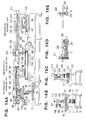
- Fig. 1 is a diagram showing a schematic construction showing a first embodiment of a whole system for dicing (cutting) a thin semiconductor wafer (semiconductor board) into thin semiconductor chips (semiconductor devices) and mounting the semiconductor chips onto a circuit board constructing an IC card or the like according to the invention.
- the system is constructed by: a separation mechanism part (separating means) 100 for dicing (cutting) a thin semiconductor wafer (semiconductor board) 10 having the thickness of 0.002 to 0.2 mm into thin semiconductor chips (semiconductor devices) 10 having the thickness of about 0.002 to 0.2 mm and for adsorbing a group 20 of thin semiconductor chips (semiconductor devices) in a row state at once by a vacuum collet 101; a separation conveyer part (conveying means) 200 for separating and inverting each thin semiconductor chip from the group 20 of thin semiconductor chips (semiconductor devices) in a row state obtained by separating the thin semiconductor wafer (semiconductor board) by the separating mechanism part 100 and for adsorbing the inverted thin semiconductor chip by a vacuum nozzle 216; and a mounting mechanism part (mounting means) 300 for positioning the thin semiconductor chip 10 adsorbed and conveyed by the vacuum nozzle 216 in the separation conveyer part 200 and mounting
- a thin semiconductor wafer 40 semiconductor circuits are formed on a chip unit basis by a regular semiconductor fabricating method on a base material such as silicon.
- the thin semiconductor wafer 40 in which the semiconductor circuits are formed in the above manner is sorted into non-defective pellets and defective pellets which can be repaired by an electric characteristics test, visual inspection, or the like.
- the defective pellet is marked or the position coordinates of the defective pellet are stored in a recording medium or a storage of an inspection system in correspondence to the item number of the thin semiconductor wafer.
- the adhesive sheet 50 On the back face of the thin semiconductor wafer 40 inspected as mentioned above, an adhesive sheet 50 which is larger than the outer shape of the semiconductor wafer 40 is adhered in a sheet adhering process.
- the adhesive sheet 50 has a sheet base material 51 formed in a thin film state which is made of a resin having elasticity such as PVC (polyvinyl chloride) or PET (polyethylene terephthalate) having the diameter larger than that of the wafer.
- a predetermined adhesive is applied, thereby forming an adhesive layer 52.
- the adhesive has the property such that the adhesive is a polyimide base material and is hardened by being irradiated with ultra violet (UV) rays and the adhesion is weakened.
- UV ultra violet
- an acrylic base material which has the property of hardening and weakening the adhesive strength under heat is also applicable.
- this adhesive agent when using this adhesive agent, this is heated instead of being irradiated with ultra violet (UV) rays.
- UV ultra violet
- the peripheral part of the adhesive sheet 50 to which the thin semiconductor wafer 40 is adhered is stretched and adhered to a metallic frame (carrier ring) 55 made of stainless steel or the like while being spread so as not to be slacked.
- the thin semiconductor wafer 40 adhered onto the adhered sheet 50 attached to the metallic frame (carrier ring) 55 is diced into thin semiconductor chips by using a thin grinder 61 as shown in Fig. 2B in a dicing process.
- the thin semiconductor wafer 40 can be diced since the adhesive sheet 50 is adhered with adhesive strength sufficient to hold at the time of dicing. Since the adhesive sheet 50 is not diced by the dicing operation, the group 20 of diced semiconductor chips are adhered to the adhesive sheet 50 by the adhesion.
- the areas in which the semiconductor chips 10 are adhered to the adhesive sheet 50 are irradiated with ultra violet (UV) rays and the adhesive 52 on the adhesive sheet 50 is hardened, thereby weakening the adhesive strength.
- UV ultra violet
- the work 60 fabricated as mentioned above is supplied to the separation mechanism part 100 and mounted and fixed onto the movable stage 61.
- Fig. 3 is a front view showing a method of peeling off the group of semiconductor chips 10 in a row and placing them in the same position every row.
- Fig. 4 is a side view of Fig. 3.
- W denotes the width of a chip peeling roller.
- the width (a) of the thin semiconductor chip 10 is consequently equal to (W + 2S).
- the group of thin semiconductor chips in a row is peeled from the adhesive sheet 50 and is placed in the same position.
- the semiconductor chip 10 is once peeled from the adhesive sheet 50 from one end toward the other end from the state shown in Fig. 6A to the state shown in Fig. 6B, and from the state shown in Fig. 6B to the state shown in Fig. 6C.
- the member 62 by linearly moving the member 62 along the group of thin semiconductor chips in a row from one end to the other end of the adhesive sheet 50 within the metallic frame 55 in a state where the member 62 is pushed up with a predetermined pressure, all of the thin semiconductor chips in the row are easily peeled from the adhesive sheet 50 and are placed in the same position without being cracked or damaged.
- (ft) denotes the tension applied on the adhesive sheet 50 when the member 62 is pushed up with a predetermined pressure.
- the peeling angle ⁇ has the relation of about ( ⁇ 1 + ⁇ 2).
- Reference character (R) denotes the radius of curvature of the member 62. It is sufficient to set the radius (R) of curvature within a range where the semiconductor chip is not damaged or cracked, for example, from about 2 to 5 mm.
- reference numeral 62 is constructed by the chip peeling roller, it can be rotatably supported.
- Fig. 7A shows change in the tension ft applied to the adhesive sheet 50 when the back face of the adhesive sheet 50 is pushed up by the member 62 from an adhesive sheet bending face 64 of the metallic frame 55 by, for instance, 3 mm.
- the axis of abscissa denotes the position of the adhesive sheet 50 adhered to the metallic frame 55.
- Reference character A shows the center position of the adhesive sheet 50.
- the axis of abscissa denotes the position in the adhesive sheet 50 adhered to the metallic frame 55.
- Reference character (A) shows the center position of the adhesive sheet 50.
- the lifting amount is, for example, 3 mm in the embodiment
- the peeling angle ⁇ increases exponentially with movement of the member 62 from the center to the peripheral part.
- the peeling angle ⁇ decreases with movement of the member 62 from the peripheral part to the center.
- the peeling force f t sin ⁇ acting on the adhesive sheet 50 from the end for the thin semiconductor chip 10 accordingly decreases with the movement of the member 62 from the peripheral part to the center.
- the pressing force acting on the member 62 also decreases with the movement from the peripheral part to the center.
- the pushing force P by the member 62 and the tension ft acting on the adhesive sheet 50 have the approximation relation of (formula 1) shown below when the frictional resistance between the member 62 and the adhesive sheet 50 is ignored.
- the tension ft acting on the adhesive sheet 50 increases by an amount corresponding to the frictional resistance, and the peeling force f t sin ⁇ naturally increases.
- P ft ⁇ (sin ⁇ 1 + sin ⁇ 2)
- the peeling force f t sin ⁇ acting on the adhesive sheet 50 is increased so as to be greater than the adhesive strength F. Even if the thin semiconductor chip 10 is positioned in the center part, it can be easily peeled from the adhesive sheet 50 and positioned in the same place.
- the tension ft acting on the adhesive sheet 50 When the force P pushing the back face of the adhesive sheet 50 by the member 62 is increased, the tension ft acting on the adhesive sheet 50 also increases. When the tension ft acting on the adhesive sheet 50 exceeds the elastic limit, however, the adhesive sheet 50 becomes slack. The tension ft acting on the adhesive sheet 50, therefore, has to be within the elastic limit. On the other hand, since the adhesive sheet 50 has orientation and the elastic limit in the flow direction (orientation direction) is larger than that in the perpendicular direction, it is necessary to set the flow (orientation) direction in the y-axis direction shown in Fig. 5 and to adhere the semiconductor wafer 40 to the adhesive sheet 50.
- the elastic limit in the y-axis direction in the adhesive sheet 50 can be increased, the force P for pushing the back face of the adhesive sheet 50 by the member 62 can be increased for the whole area, the peeling force f t sin ⁇ is increased, and the group of thin semiconductor chips in a row can be easily peeled from the adhesive sheet 50.
- the crack condition of the thin semiconductor chip having the thickness of about 0.002 to 0.2 mm relates to a case based on the relation of (formula 3) shown as follows where the semiconductor chip is not peeled from the adhesive sheet 50 and bending equal to or less than the radius p of curvature is applied to the semiconductor chip.
- 1/ ⁇ M/(EI) where M is a bending moment which can be permitted to the thin semiconductor chip, E is Young's modulus of the semiconductor chip, and I is geometrical moment of inertia by the thin semiconductor chip.
- the radius R of curvature of the member 62 pushing up the back face of the adhesive sheet 50 is equal to or less than the radius ⁇ of curvature obtained from the relation of (formula 3), for example, about 2 to 5 mm, however, when the peeling force f t sin ⁇ greater than the adhesive strength F is acted from one end of the semiconductor chip by the tension ft occurring in the adhesive sheet 50, the thin semiconductor chip is peeled from the adhesive sheet without being cracked.
- a first embodiment of the separation mechanism part 100 according to the invention will be described with reference to Figs. 8, 9, and 10.
- the work 60 is ejected from a cassette housed in a magazine (not shown) and is loaded onto the stage 61.
- the reason why the work is inserted into cassette or the like and is housed in the magazine without being exposed to the atmosphere is that, if the work 60 is left naked, as shown in Fig. 2C, the area adhered to the adhesive sheet 50 in the semiconductor chip 10 is irradiated with ultra violet rays (UV) to harden the adhesive 52 in the adhesive sheet 50 and the adhesive strength F is increased although it is slight.
- UV ultra violet rays
- the adhesive strength F is maintained to be almost constant by inserting the work 60 in the cassette or the like and housing in the magazine or the like so that the adhesive of the adhesive sheet does not change chemically as mentioned above. Consequently, only by pushing the back face of the adhesive sheet 50 by the member 62, the group of semiconductor chips in a row state can be easily peeled off and placed in the same position without being cracked or damaged.
- change in the environment (for example, the temperature) of the magazine and the separation mechanism part 100 is prevented, the characteristics of the adhesive of the adhesive sheet after irradiation of UV are not changed and the adhesive force F can be maintained to be almost constant.
- Reference numeral 61 is the stage on which the work 60 ejected from the cassette housed in the magazine (not shown) is put and is sandwiched by a fixing means 65.
- the stage 61 is supported by a column 77 so as to be movable in the x-axis direction and is constructed to be moved step by step at the pitch of the thin semiconductor chip row by a feeding mechanism 78 having a drive source such as a motor controlled by a controller 80 in the x-axis direction shown in Fig. 5.
- the orientation direction of the adhesive sheet 50 is set in the y-axis direction.
- Reference numeral 76 denotes a base; 74 a guide stage mounted on the base 76; 72 a stage for reciprocating the member 62 in the y-axis direction, which is reciprocated in the y-axis direction on the guide stage 74 by a feeding mechanism 73 connected to an output of a drive source 75 such as a motor controlled by the controller 80; 67 a rod member which has an end to which the member 62 is attached and is supported so as to be movable in the vertical direction by a supporting member 68 to be pushed up by a spring member 66; 69 a vertical moving member to which the supporting member 68 is attached and which is moved vertically above the stage 72 by a feeding mechanism 70 connected to the output of a drive source 71 such as a motor controlled by the controller 80; 81 a storage for storing a control program, control data, and the like, which is connected to the controller 80 constructed by a computer or the like; and 82 a display means which outputs and displays the control data and the like and is connected
- the stage 61 is moved in response to a control command from the controller 80 and the group of thin semiconductor chips in the row at the end in the x-axis direction is positioned so as to face the line on which the member 62 is reciprocated. Coordinate information of the work 60 is inputted by using input means 83 into the controller 80. A displacement amount (position information) of the stage 61 is fed back from the feeding mechanism 78 to the controller 80. Consequently, as mentioned above, the stage 61 can be positioned by the control command from the controller 80. As shown in Figs.
- the stage 72 is moved to the right end by driving the driving source 75 on the basis of the control command from the controller 80 and the member 62 is positioned to the right end of the group of the thin semiconductor chips in one row at the end in the x-axis direction.
- the supporting member 68 is lifted by driving the driving source 71 by a control command from the controller, the back face of the adhesive sheet 50 is pushed up by the member 62 with the pressure of the spring member 66, and the tension ft is given to the adhesive sheet 50 as shown in Fig. 3.
- the stage 72 is moved from the right end by driving the driving source 75 to the state shown in Fig.
- the stage 72 is moved from the left end to the state shown in Fig. 9C and Fig. 13B. Subsequently, the stage 72 is moved from the left end to the state shown in Fig. 9D and is further moved to the right end, thereby reciprocating the stage 72. Further, as shown in Fig. 10A, the supporting member 68 is lowered, thereby peeling off the group of the thin semiconductor chips in one row at the end in the x-axis direction from the adhesive sheet 50 and placing it in the same position. In this case, it is unnecessary to reciprocate the stage 72. In order to certainly peel off the adhesive sheet 50, however, it is preferable to reciprocate the stage 72. In such a state, as shown in Fig.
- the vacuum collet 101 is lowered by driving a drive source 102 such as a cylinder by a control command from the controller 80, the group 20 of the thin semiconductor chips in one row is adsorbed by the vacuum collet 101 and is lifted, thereby separating the group 20 of the thin semiconductor chips in one row from the adhesive sheet 50 as shown in Fig. 10C.
- the vacuum collet 101 conveys the adsorbed group 20 of the thin semiconductor chips in one row to the separation conveyer part 200 by a feeding mechanism 109 by driving a drive source 108 in response to a control command from the controller 80 as shown in Fig. 11A, puts the group 20 of the semiconductor chips on a conveyer 201 as shown in Fig. 11B, and is returned to the separation mechanism part 100.
- the stage 61 is moved by an amount corresponding to the pitch of the group of the thin semiconductor chips of one row and the movement of the stage 72 and the supporting member 68 is controlled, thereby peeling off the group 20 of thin semiconductor chips of the next row from the adhesive sheet 50 by the member 62 and separating from the adhesive sheet 50 by the vacuum of the vacuum collet 101 as shown in Fig. 13C.
- the groups of the thin semiconductor chips of all of the rows can be peeled from the adhesive sheet 50, separated from the adhesive sheet 50 by the adsorbing operation of the vacuum collet 101, conveyed to the separation conveyer part 200, and put on the conveyer 201.
- the forces P for pushing up the adhesive sheet by the member 62 in the peripheral and central parts including variations in the tension of the adhesive sheet 50 are preset by theory, experiment, or the like with respect to the groups of the thin semiconductor chips of all of the rows, and the set pushing force P is inputted by using the input means 83 or the like and is stored in the storage 81 or the like.
- the forces P for pushing the adhesive sheet by the member 62 in the peripheral and central parts can be calculated by the CPU in the controller 80 and stored in the storage 81 or the like with respect to the groups of the thin semiconductor chips in all of the rows.
- the controller 80 can properly set the force P for pushing the adhesive sheet by the member 62 both in the peripheral and central parts with respect to the groups of the thin semiconductor chips in all of the rows in accordance with a change in flexibility (for example, a compression amount) of the spring member 66.
- the groups of the thin semiconductor chips in all of the rows can be, therefore, certainly peeled off without damaging the adhesive sheet 50.
- Reference numeral 109 indicates the base in which a supporting member 103 is movably guided and supported between the separation mechanism part 100 and the separation conveyer part 200.
- Reference numeral 108 denotes the drive source such as a motor for moving the supporting member 103 between the separation mechanism part 100 and the separation conveyer part 200 by a feeding mechanism.
- a movable block 105 is supported so as to be movable in the vertical direction, the drive source 102 such as a cylinder is mounted, an output of the drive source 102 is connected to the movable block 105 and the movable block 105 is moved vertically.
- the movable block 105 supports the vacuum collet 101 via a spring member 106 so as to be vertically movable.
- the vacuum collet 101 is constructed in such a manner that holes for attraction are opened in accordance with the group of the semiconductor chips in a row peeled from the adhesive sheet 50 and placed, even if the holes are not closed by the semiconductor chips, the semiconductor chips are attracted by the flow of air so as to assure the attraction by the other holes. With such a construction, even if the number of chips of the group of the semiconductor chips in one row is changed, the attraction is not reduced and the group of the semiconductor chips in one row can be adsorbed by the vacuum collet 101 at once. As shown in Fig.
- the movable block 105 and also the vacuum collet 101 are descended by driving the drive source 102 such as a cylinder in response to a control command from the controller 80.
- the drive source 102 such as a cylinder
- the end of the vacuum collet 101 is allowed to contact with or come close with a small gap the group 20 of the thin semiconductor chips in one row peeled from the adhesive sheet 50 and placed and the group 20 of thin semiconductor chips in the row is adsorbed by the vacuum collet 101.
- the vacuum collet 101 is lifted with the rise of the movable block 105. In this manner, the group 20 of thin semiconductor chips in one row is separated from the adhesive sheet 50 as shown in Fig. 10C. As shown in Fig.
- the vacuum collet 101 which vacuums the group 20 of thin semiconductor chips in one row is moved together with the supporting member 103 to the separation conveyer part 200 by the feeding mechanism 109 by driving the drive source 108 in response to the control command from the controller 80.
- the drive source 102 such as a cylinder is driven by a control command from the controller 80 to descend the movable block 105 and the vacuum collet 101.
- the spring member 106 is compressed, the group 20 of thin semiconductor chips in one row adsorbed by the end of the vacuum collet 101 is come into contact with the conveyer, and the vacuum of the vacuum collet 101 is canceled, thereby enabling the group 20 of thin semiconductor chips in one row to be put on the conveyer 201 as shown in Fig. 11B.
- a second embodiment in which the vacuum collet 101 in the separation mechanism part 100 according to the invention is removed will be described.
- a point different from the first embodiment is such that the forces P for pushing up the adhesive sheet by the member 62 in both of the peripheral and central portions are controlled more accurately with respect to the groups of thin semiconductor chips in all of rows.
- Reference numeral 84 denotes a pressure sensor attached to the supporting member 68, which optically or magnetically senses a displacement of the member 62, thereby sensing the pressure P for pushing up the adhesive sheet 50 by the member 62 via the spring member 66.
- the pressure sensor 84 can be constructed by a distortion gauge or the like and provided between the spring member 66 and the supporting member 68 so as to sense the pressure P for pushing up the adhesive sheet 50 by the member 62 via the spring member 66. It is also possible to construct in such a manner that the spring member 66 is removed from the member 62 and the pressure sensor 84 is directly attached to the lower end of the member 62 so as to sense the pressure P.
- Reference numeral 85 denotes a displacement sensor attached on the stage 72, which optically or magnetically senses displacement of the member 62, thereby sensing flexibility (h) of the adhesive sheet 50.
- the reason why the flexibility (h) of the adhesive sheet 50 can be sensed by the displacement sensor 85 is because there is no fluctuation in distance between the stage 61 on which the work 60 is put and the stage 72.
- the displacement sensor 85 senses it and the sensed position can be used as a reference position where there is no flexibility in the adhesive sheet 50.
- the displacement sensor 85 can be constructed by an air micro which is attached to the tip of the stage 72 and directly measures the flexibility near the back face of the adhesive sheet 50 to which the tip of the member 62 acts.
- the member 62 when the member 62 is lifted by driving the drive source 72 with the pressure P for pushing up the adhesive sheet 50 by the member 62 sensed by the pressure sensor 84 and the flexibility (h) of the adhesive sheet 50 sensed by the displacement sensor 85, thereby pushing up the back face of the adhesive sheet 50, it can be controlled so that the tension ft applied on the adhesive sheet 50 does not exceed the elastic limit and the separation force f t sin ⁇ exceeds the adhesive strength F in the whole area of the adhesive sheet 50.
- the group of thin semiconductor chips in a row can be easily peeled off and placed in the same position without being cracked or damaged.
- the force P for pushing up the back face of the adhesive sheet 50 by the member 62 can be controlled in accordance with the slack of the adhesive sheet. Consequently, the group of thin semiconductor chips in one row can be easily peeled from the adhesive sheet 50 by applying a desired tension to the adhesive sheet 50 without being cracked or damaged.
- the controller 80 can obtain the information (11, 12) that the stage 72 is displaced in the y-axis direction and the member 62 is positioned in the y-axis direction from a displacement sensor such as encoder provided for the drive source 75.
- the controller 80 can also obtain the information (13 + W/2, 14 + W/2) that the stage 61 is displaced in the x-axis direction and the member 62 is positioned in the x-axis direction from a displacement sensor such as an encoder provided for the drive source 78.
- the controller 80 can calculate the angles ⁇ 1 and ⁇ 2 between the adhesive sheet 50 and the under face 64 of the metallic frame 55 shown in Fig. 3 from the positional information (11, 12) in the y-axis direction of the member 62 obtained from the displacement sensor such as an encoder provided for the drive source 75 and the flexibility (h) of the adhesive sheet 50 sensed by the displacement sensor 85. Further, since the pressure P for pushing up the adhesive sheet 50 by the member 62 can be sensed by the pressure sensor 84, the tension ft acting on the adhesive sheet 50 can be calculated from (formula 1).
- the controller 80 controls the drive source 71 so that the tension ft applied on the adhesive sheet 50 is within the elastic limit and the peeling force f t sin ⁇ sufficiently exceeds the adhesive strength F in the whole area of the adhesive sheet 50, only by pushing up the back face of the adhesive sheet 50 by the member 62 and moving the member 62 in the y-axis direction, the group of thin semiconductor chips in a row can be easily peeled off and placed in the same place without cracking or damaging them.
- the spring member 66 in the second embodiment as mentioned above can also play a role to soften the impact when the tension is applied to the adhesive sheet 50 by pushing up the member 62.
- the stages 61 and 72 are controlled in a manner similar to the first embodiment as shown in Fig. 13.
- the stage 72 is moved to the right end by driving the drive source 75 on the basis of the control command from the controller 80, thereby positioning the member 62 to the right end of the group of thin semiconductor chips in one row at the end in the x-axis direction.
- the supporting member 68 is lifted by driving the drive source 71 and the back face of the adhesive sheet 50 is pushed up by the member 62 with the pressure of the spring member 66, thereby applying the tension ft to the adhesive sheet 50 as shown in Fig. 3.
- the drive source 75 is driven to reciprocate the stage 72 by moving from the right end to the left end as shown in Fig.
- the vacuum collet 101 descends as shown in Fig. 10B, vacuums the group 20 of thin semiconductor chips in one row and is lifted as shown in Fig. 10C, thereby separating the group 20 of thin semiconductor chips in one row from the adhesive sheet 50.
- the vacuum collet 101 conveys the adsorbed group 20 of thin semiconductor chips in one row to the separation conveyer part 200 and puts them on the conveyer 201, and is returned to the separation mechanism part 100.
- the stage 61 is moved by an amount corresponding to the pitch of the group of thin semiconductor chips in one row, the movement of the stage 72 and the supporting member 68 is controlled, and the group 20 of thin semiconductor chips in the next row is peeled from the adhesive sheet 50 by the member 62 as shown in Fig. 13C and is separated from the adhesive sheet 50 by the adsorbing operation of the vacuum collet 101.
- the groups of thin semiconductor chips in all of the rows are peeled from the adhesive sheet 50 in serial order, separated from the adhesive sheet 50 by the adsorbing operation of the vacuum collet 101, conveyed to the separation conveyer part 200, and placed on the conveyer 201.
- FIG. 14 A third embodiment in which the vacuum collet 101 is removed from the separation mechanism part 100 according to the invention will be described with reference to Fig. 14.
- the adhesive sheet 50 is adhered to the metallic frame 55 and, after that, the semiconductor wafer 40 is diced into the semiconductor chips 10, and variations in the tension of the adhesive sheet 50 adhered to the metallic frame 55 occurring until the work 60 in which the adhesion of the semiconductor chips 10 to the adhesive sheet 50 is weakened by the UV irradiation is loaded onto the stage 61 are suppressed.
- Reference numeral 91 denotes a ring-shaped groove formed in the stage 61 along the inner periphery of the metallic frame 55 of the adhesive sheet 50 adhered to the metallic frame 55; 92 a ring-shaped pressing member using a pressure of a spring member 93; 95 a shaft having a stopper formed at the upper end of the ring-shaped pressing member 92; 94 a supporting member for supporting the ring-shaped pressing member 92 so as to be movable in the vertical direction and for supporting the shaft 95 so as to be vertically slidable; and 96 a cylinder attached to the stage 61 by an attaching member 97, which connects an output to the supporting member 94 and allows the ring-shaped pressing member 92 to escape upward so as to set the work 60 onto the stage 61.
- the back face of the outer peripheral part of the adhesive sheet 50 adhered to the metallic frame 55 in the work 60 put on the stage is supported by both ends of the ring-shaped groove 91.
- the ring-shaped pressing member 92 is pressed from the surface side of the peripheral part of the adhesive sheet 50 with the pressure given by the spring member 93 and the adhesive sheet 50 is stretched toward the inside of the groove 91, thereby enabling a predetermined tension to be given to the adhesive sheet 50.
- the spring member 93 with little compressing fluctuation by the displacement is required to be used.
- a part supporting the back face of the adhesive sheet 50 formed in the ring-shaped groove 91 is required to be formed in a circular shape in cross section so as to reduce the frictional resistance. If the frictional resistance is not reduced only by forming the part supporting the back face of the adhesive sheet 50 formed in the ring-shaped groove 91 in a circular shape in cross section, it is desired to cover the surface with a material having a little frictional resistance.
- the ring-shaped pressing member 92 is descended together with the supporting member 94 by the cylinder 96 in response to the drive command from the controller 80, the ring-shaped pressing member 92 is pressed by the pressure given the spring member 93, and the adhesive sheet 50 is stretched into the groove 91, thereby enabling a predetermined tension to be given to the adhesive sheet 50.
- the drive source 71 is driven in response to the drive command from the controller 80, the supporting member 68 is raised by a desired displacement amount, and the back face of the adhesive sheet 50 is pushed up by the member 62 with the pressure given the spring member 66 by a desired displacement amount (h), thereby enabling the tension ft to be given to the adhesive sheet 50 without detecting the pressing force P as shown in Fig. 3.
- a fourth embodiment of the separation mechanism part 100 according to the invention will be described with reference to Fig. 15.
- the fourth embodiment is different from the first, second, and third embodiments with respect to the following point.
- the group 20 of semiconductor chips in one row peeled from the adhesive sheet 50 and placed in the same position in the first and second embodiments are separated from the adhesive sheet 50 by lifting the group 20 of semiconductor chips in only one row by the tips of the needles 112 via the adhesive sheet 50 from a state shown in Fig. 15B to a state shown in Fig. 15C and is allowed to contact with the vacuum collet 101 which faces from the above and is adsorbed by the vacuum collet 101.
- the block 110 on which the needles 112 are vertically formed in accordance with the group 20 of semiconductor chips in one row is supported so as to be movable in the vertical direction on the stage 74.
- the block 110 is connected to the output of a drive source 111 mounted on the stage 74 and the drive source 111 is driven on the basis of the control command from the controller 80, thereby enabling the block 110 to be moved vertically. Consequently, as shown in Fig. 15A, in a manner similar to the first and second embodiments, by reciprocating the member 62 in the y-axis direction in a state where the member 62 is lifted to push up the adhesive sheet 50 in the work 60, the group 20 of semiconductor chips in one row is peeled from the adhesive sheet 50 and is placed in the same position.
- the block 110 is lifted.
- the group 20 of semiconductor chips in one row peeled by the needles 112 vertically formed on the block 110 is slightly lifted and separated from the adhesive sheet 50.
- the movable block 105 is descended by driving the drive source 102 such as a cylinder by the control command from the controller 80 and the vacuum collet 101 is also descended.
- the spring member 106 is contracted to make the end of the vacuum collet 101 come into contact with the group 20 of thin semiconductor chips in one row slightly apart from the adhesive sheet 50 and the group 20 of thin semiconductor chips in one row is adsorbed by the vacuum collet 101.
- a state shown in Fig. 15D is obtained.
- the operation after that is similar to that in the first embodiment as shown in Figs. 11A and B.
- the group 20 of thin semiconductor chips in one row peeled from the adhesive sheet 50 and placed in the same position is further slightly lifted up by the needles 112. Consequently, even if there is a semiconductor chip which is not peeled from the adhesive sheet 50 by chance, it can be certainly peeled from the adhesive sheet 50 and adsorbed and lifted up by the vacuum collet 101. Since a separation force acts on a semiconductor chip which is not sill peeled from the adhesive sheet 50 even after adsorbed and lifted by the vacuum collet 101, the fourth embodiment can be sufficiently practically used also in the first and second embodiments.
- the separation conveyer part 200 comprises the conveyer 201, a sensor 202, a sensor 203, a rotating member 208 with a nozzle, an image pickup means 209, and a conveying mechanism 230.
- the conveyer 201 is provided on a base 218 and conveys the group 20 of thin semiconductor chips (semiconductor devices) in a row which is to be conveyed and put by the vacuum collet 101 in the separation mechanism part 100.
- the sensor 202 senses a marked defective chip conveyed by the conveyer 201 and senses that a space in which the group 20 of thin semiconductor chips (semiconductor devices) is carried by the conveyer 201 and put by the vacuum collet 101 can be assured.
- the sensor 203 senses that the semiconductor chip conveyed by the conveyer 201 has come to the separation position.
- the rotating member 208 with a nozzle has: a discharging means constructed by a chute 206 and a housing container 207 to eject the defective semiconductor chip when the sensor 203 senses that the defective semiconductor chip sensed by the sensor 202 has come to the separation position; and a nozzle for attracting and inverting the non-defective semiconductor chips sensed by the sensor 203 and which is indexed by a drive source 220.
- the image pickup means 209 is provided for the rotating member 208 and measures the outer shape of the semiconductor chip 10 adsorbed by the nozzle which is expanded and contracted.
- the conveying mechanism 230 vacuums the semiconductor chips 10 adsorbed by the nozzle 216 expanding and contracted by a drive means such as a cam mechanism provided for the rotating member 208 and inverted by the index of the rotating member 208 and conveys the semiconductor chips 10 to the mounting mechanism part 300.
- the conveying mechanism 230 has a moving unit 210 which moves along a guide 212, a drive source 211 for moving the moving unit 210 via a feeding mechanism 213, and a block 215 with a vacuum nozzle to which the vacuum nozzle 216 is attached supported on the moving unit 210 so as to be movable in the vertical direction by a drive source 214 such as a cylinder.
- the sensors 202, 203, image pick means 209, drive source 217 for driving the conveyer 201, index drive source 220 of the rotating member 208, and drive sources 211 and 214 of the conveying mechanism 230 are connected to the controller 80.
- the controller 80 drives the various drive sources 217, 220, 211, and 214 in accordance with information obtained from the sensors 202, 203, the image pickup means 209, and the like.
- the group 20 of semiconductor chips is conveyed from the separation mechanism part 100 and is put on the conveyer 201 by the vacuum collet 101.
- the marked defective semiconductor chip is detected by the sensor 202.
- the nozzle provided for the rotating member 208 to be indexed is extended and descended and vacuums the semiconductor chip which has come to the separation position.
- the outer shape of the semiconductor chip adsorbed by the nozzle when the rotating member 208 is indexed is measured by the image pickup means 209 and the information is inputted to the controller 80.
- the image pickup means 209 obtains an image of the side on which an electrode 11 is not formed of the semiconductor chip, so that information of only the outer shape is obtained.
- the semiconductor chip 10 is adsorbed by the vacuum nozzle 216 on the basis of the information. That is, as shown in Figs. 18C and D, positional information ( ⁇ x, ⁇ y) for the vacuum nozzle 216 shown by a chain line in Fig. 18D in the semiconductor chip 10 adsorbed by the vacuum nozzle 216 shown by a solid line is obtained from the information of only the outer shape measured by the image pickup means 209 and is inputted to the controller 80.
- the chip adsorbed by the nozzle of the rotating member 208 and inverted by the index of the rotating member 208 is adsorbed by the vacuum nozzle 216 in the conveying mechanism 230 and is carried to the mounting mechanism part 300.
- the semiconductor chip adsorbed by the vacuum nozzle 216 and conveyed by the conveying mechanism 230 is put on X-Y stages 302 and 303 and can be mounted on the circuit board 30 constructing an IC card or the like positioned by the X-Y stages 302 and 303.
- the semiconductor chip it is necessary to position and mount the electrode 11 formed on the semiconductor chip and the electrode formed on the circuit board 30.
- An image pickup means 306 is installed in a passage through which the semiconductor chip adsorbed by the vacuum nozzle 216 is conveyed by the conveying mechanism 230, picks up the image of the side on which the electrode 11 is formed in the semiconductor chip, measures the positions (d1x, d1y) (d2x, d2y) of the electrode (pad) 11 by using the outer shape as a reference, and inputs the data into the controller 80.
- the semiconductor chip 10 is conveyed by a determined distance to the mounting mechanism part 300 by the conveying mechanism 230 by using the vacuum nozzle 216 as a reference.
- the position information of each electrode 11 formed on the semiconductor chip using the vacuum nozzle 216 as a reference is necessary.
- the position information of each electrode 11 can be calculated on the basis of the position information (d1x, d1y) (d2x, d2y) of each electrode (pad) 11 obtained by using the outer shape picked up the by the pickup means 306 as a reference and outer shape position information ( ⁇ x, ⁇ y) picked up by the image pickup means 209 and obtained by using the vacuum nozzle as a reference.
- the position information of the electrode 11 preliminarily formed on the semiconductor chip and the electrode formed on the circuit board to be connected is inputted to the controller 80 and is stored into, for example, the storage 81.
- the controller 80 positions the X-Y stages 302 and 303 by driving drive sources 304 and 305 which drive the X-Y stages 302 and 303 on the basis of the position information of the electrode formed on the circuit board and the calculated position information of each electrode 11 formed on the semiconductor chip obtained by using the vacuum nozzle 216 as a reference, thereby enabling the electrode formed on the circuit board and the electrode formed on the semiconductor chip to be connected by using a bonding material or the like.
- the defective semiconductor chip is sensed by the sensor 202 in the separation conveyer part 200 since the position information in the semiconductor wafer coordinates (shown in Fig. 17C) of the defective semiconductor chip has been sensed by the test as shown in Figs. 17A and B, if the position information is inputted to the controller 80, the defective semiconductor chip can be removed in the separation position by the ejecting means 207, 207.
- the separation mechanism part 100 is arranged in the vertical direction
- a plurality of the separation mechanism part 100 can be arranged also in the lateral direction.
- the separation mechanism part 100 is arranged laterally, the conveying operation of the vacuum collet 101 shown by 103 in Fig. 1 to the separation conveyer part 200 has to be performed in both of the vertical and lateral directions.
- a plurality of separation mechanism parts 100 can be arranged side by side. Consequently, the group 20 of semiconductor chips in rows can be supplied more to the separation conveyer part 200.
- a second embodiment of the whole system for dicing (cutting) a thin semiconductor wafer (semiconductor substrate) into thin semiconductor chips (semiconductor devices) and mounting the semiconductor chips onto a circuit board constructing an IC card or the like according to the invention will be described with reference to Figs. 19 to 29.
- a part largely different from the first embodiment is a separation mechanism part 100'.
- the operation of the separation mechanism part (separation means) 100' will be described with reference to Fig. 19.
- the whole surface on which the electrode 11 is formed of the semiconductor chip obtained by the dicing operation is strongly held by a chuck 150 for the work 60.
- the chuck 150 has a chuck face member 151 in which grooves 152 for vacuum adsorption are formed on the surface in correspondence to the semiconductor chips 10 and the grooves 152 are communicated with a vacuum source 153. It is not always necessary to construct the chuck 150 by a vacuum chuck. Any member can be used as long as the semiconductor chips can be strongly held. It can be also constructed by a magnet chuck or a frozen chuck (by a deep-freezing process which deep-freezes water on the surface of the chuck, the group of the semiconductor chips is fixed and it is removable by an unfreezing process).
- the adhesive sheet near the inner periphery of the metallic frame 55 for the work 60 which is strongly held by the chuck 150 is diced by rotating a cutter 155 and the metallic frame 55 is cut off from the adhesive sheet 50.
- the chuck 150 and a clamp means 160 constructed by a pair of clamp rollers are made relatively close to each other and one end of the adhesive sheet 50 from which the metallic frame 55 is cut is clamped by the clamp means 160 made of the pair of clamp rollers.
- the whole clamp means 160 is turned by 180° around an axis 161 as a center as shown by the arrow 162. As shown in Fig. 19C, the end of the adhesive sheet 50 is lifted upward.
- the adhesive sheet 50 adhered with the adhesive strength which is remarkably deteriorated by the UV irradiation to the group of the thin semiconductor chips is pulled laterally and is peeled from the group of thin semiconductor chips held by the chuck 150 without cracking the group of thin semiconductor chips.
- the adhesive sheet is peeled from the group of the thin semiconductor chips by the pulling force acting on the adhesive sheet, the adhesive sheet is peeled from one end of the semiconductor chip to the other end. Consequently, the adhesive sheet 50 can be peeled off without cracking and damaging any of the thin semiconductor chips held by the chuck 50. Further, when the direction of peeling the thin semiconductor chips 10 from the adhesive sheet 50 is set from the corner of the semiconductor chip, the adhesive sheet 50 can be peeled with weaker force.
- a wedge-shaped peeling angle fixing jig 165 is used as shown in Figs. 21 A and B.
- the wedge-shaped peeling angle fixing jig 165 has roles of assuring the peeling angle ⁇ and focusing the peeling force by justifying a peeling location linearly against the group of the diced thin semiconductor chips.
- a top end 165a of the wedge-shaped peeling angle fixing jig 165 prevents the semiconductor chips 10 from cracking by avoiding the peeling force focusing at one point and forming the predetermined curved face (approximately 0.5 to 2.0 mm in radius). With the smaller radius of the curved face, it is easy to peel since the peeling force is focused. As a matter of course, with the thinner adhesive sheet, the smaller is the radius of the curved face, thus the peeling force is focused.
- Figs. 22A and B is the same to Figs. 19A and B.
- the peeling angle fixing jig 165 is located in the right end to be close to the surface of the adhesive sheet 50. While relatively moving the chuck 150 and the clamp means 160, the whole clamp means is turned about an axis 161 by 180° as shown by the arrow 162. As shown in Fig. 22C, the end of the adhesive sheet 50 is lifted upward and bent at the top end 165a of the peeling angle fixing jig.
- the adhesive sheet 50 is peeled in serial order from each end of the semiconductor chips 10.
- a moving speed of the whole clamp means 160 may be approximately double the speed of peeling angle fixing jig 165.
- the peeling angle fixing jig 165 it is possible to assure the peeling angle ⁇ , to justify a peeling location linearly against the group of the diced thin semiconductor chips, to focus the peeling force, and to peel the adhesive sheet 50 smoothly without cracking each thin semiconductor chip.
- the directions of peeling the adhesive sheet 50 against the group of the diced semiconductor chips there are the direction in which the semiconductor chips are arranged as shown in Fig. 21A, and the direction in which the plane surface tilts against the direction of semiconductor chips arranged as shown in Fig. 21B. Since in the case shown in Fig. 21B, the adhesive sheet begins to be peeled from the corner against each conductor chip, it is supposed that it is easier to be peeled than the case shown in Fig. 21A.
- a porous absorptive plate 153 is provided on the absorptive surface, there is no need to fill absorptive holes except those for the group of the semiconductor chips and to adjust an arrangement of absorptive holes for the semiconductor chips. However, if the porous absorptive plate 153 is used, the absorptive force will be lowered.
- a fluorine resin film on the adsorptive surface provided a plurality of pinhole-shaped adsorptive holes, it is possible not to damage a circuit surface since the adsorptive force can be assured as well as the circuit surface formed electrodes or the like of the semiconductor chips is adsorbed by assuring the holding force to some extent.
- a surface of the fluorine resin film bears the electrical charge, at times it is neutralized by ion blowing using an ion ejection means 166 and thus gives no influence to the semiconductor chips.
- a vacuum adsorptive hole 156 is provided in the periphery (frame) of the chuck 150 and a needle spicule 157 is provided in the periphery (frame) of the chuck 150.
- a needle spicule 157 is provided in the periphery (frame) of the chuck 150.
- the periphery of the adhesive sheet 50 can be firmly fixed to the periphery (frame) 159 of the chuck 150. In case when the adhesive sheet can be fixed by the vacuum adsorption, the needle spicle is not needed.
- the separation mechanism part (separating means) 100' is constructed as specifically shown in Fig. 28.
- the work 60 is supplied onto the supporting member 170 with the side of the adhesive sheet 50 facing upward and the metallic frame 55 is positioned and fixed.
- the chuck 150 is attached onto the supporting member 171 which is elevated by the drive source 173.
- the supporting member 171 is supported movably in the vertical direction by a stage 172 which is supported so as to be movable in the lateral direction on a base 175 by feeding operation of a drive source 174.
- a supporting member 179 which supports a rotating member 178 to which the cutter 155 is attached is descended.
- a drive source 180 By rotating the rotating member 178 by driving a drive source 180, the metallic frame 55 is diced from the adhesive sheet 50.
- Reference numeral 181 denotes a member for supporting the supporting member 179 movably in the vertical direction.
- the cutter 155 is lifted and the chuck 150 is simultaneously descended by driving the drive source 173 and is moved laterally to the clamp means 160 constructed by the pair of clamps which wait for the chuck 150 by driving the drive source 174.
- the clamp means 160 comprises a moving mechanism having a drive source for moving the clamp means 160 laterally and a rotating means having a drive source for turning the clamp means 160 by 180°.
- one end of the adhesive sheet 50 is clamped by the clamp means 160, the adhesive sheet 50 is peeled from the group of thin semiconductor chips held by the chuck 150 by a relative operation of the chuck 150 and the clamp means 160, the peeled adhesive sheet is adsorbed by the vacuum means 176 and is removed.
- the chuck force of the chuck 150 to the group of thin semiconductor chips is weakened, the face opposite to the electrode face is adsorbed by the vacuum collet 101 every group of semiconductor chips of one row and the group of semiconductor chips is put on the conveyer 201 with the electrode face facing downward.
- the inverting mechanism 208 shown in Figs. 1 and 16 is unnecessary.
- Reference numeral 250 is a transfer mechanism for transferring the non-defective semiconductor chips conveyed by the conveyer 201 to the conveyer 251 and aligning the semiconductor chips on the conveyer 251.
- the mounting mechanism part (mounting means) 300 is similar to that in the first embodiment.
- the thin semiconductor wafer is diced into thin semiconductor chips and the thin semiconductor chips can be mounted onto the circuit board which is used to form an IC card or the like at high speed while shortening tact time without cracking or damaging the thin semiconductor chips.
- the separation mechanism 100' arranged in lengthwise it is required to add a mechanism which can change a direction of the movement from the lengthwise direction to the lateral direction of conveying the vacuum collet 101 in the vacuum collet part 120 comprising the conveyer mechanism as same as in a first embodiment.
- the conveying movement shown by a reference numeral 130 of the vacuum collet 101 to the separation conveyer part 200 shown in Fig. 1 needs the lengthwise and the lateral directions.
- the separation mechanism part 100' arranged laterally allows a plurality of the separation mechanism part 100' to be provided in line, and thus it is possible to provide more groups of the semiconductor chips peeled from the adhesive sheet 50 to the separation conveyer part 200'.
- Fig. 30 is a plan view of an IC card.
- Fig. 31 is an A-B-C-D cross sectional view of Fig. 30.
- Fig. 32 is an enlarged cross sectional view of a principal part of Fig. 31.
- an IC card 400 comprises a film 410, a conductor pattern 420 formed on and a film 410, and an electronic component 430 such as an IC chip connected to the conductor pattern 420 via an access terminal.
- a part of the conductor pattern 420 constitutes a loop-shaped antenna coil 422 which is connected to the electronic component 430 (10) by the conductor pattern.
- the number of winding turns of the loop-shaped antenna is optional.
- the electronic component 430 is fixed with a temporary fixing fluid 440 against the film 410.
- a width D1 and a length L1 of the IC card 400 is 54 mm and 85.6 mm respectively, for example, which are the same with those of a credit card or a telephone card.
- a square electronic component 430(10), whose width D3 is 3 mm for example is used.
- a width D3 of the antenna coil 422 and a width D4 of the conductor pattern 420 are 0.2 mm, for example.
- the access terminal 432 is 15 mm square for example which is shorter than a width of the conductor pattern 420.
- a cross sectional structure of the IC card will be explained with reference to Fig. 31.
- the conductor pattern 420 and the antenna coil 422 are printed on the film 410 of the IC card 400.
- the access terminal 432 of the electronic component 430 is directly connected to the conductor pattern 420, thereby being electrically continuous.
- the film 410 and a cover film 460 are laminated and fixed using adhesives like Hot Melt in a state of putting the conductor pattern 420 and the electronic component 430 between.
- printed surfaces 470 and 470 for a design and the like are printed. From above structure, a thickness H of the IC card 400 is realized to be approximately 0.25 mm thin.
- Structural features of such IC card 400 have the following points. That is, a formation of the conductor patterns 420 and 422 by a conductor paste such as Ag and Cu has a single layered structure which is only formed on a single side of the film 410.
- a method tried presently in which a conductor pattern, especially, an antenna coil is to be formed on both sides of a film can eliminate a screen-printing step for forming a conductor pattern on the single side and a following drying step.
- the IC card can be thinner to be 0.25 mm in thickness.
- a method for fabricating the IC card comprises: a printing step P10 for forming the conductor pattern 420 and the antenna coil 422 on the film 410 by printing in a screen-printing method, for example, with the conductor paste Ag, Cu and the like; a drying step P20 for drying the conductor 420 and the antenna 422 by linearly scanning and irridating a laser beam against the printed conductor pattern 420 and the antenna coil 422, moving the conductor pattern 420 and the antenna coil together with above mentioned film 410 and instantly evaporating the conductor paste; a step P40 for printing or applying a temporally fixing agent 440 to a position to mount the electronic component (10) using a dispenser or the like; a step 50 for laminating by heating/pressing and concurrently connecting electronic component; a cutting step P60 for cutting a sheet laminated in the step P50 into a size of the IC card; a step P70 for printing a design and the like 470 and 472 on both sides; an inspection step P80 for inspecting reading and
- a transparent or white PET polyethylene terephthalate
- PVC polyvinyl chloride
- plastic such as polyimide
- the thickness of approximately 75 ⁇ m to 100 ⁇ m, for example is used.
- a film is provided in the state of roll of 250mm in width for a system of fabricating the IC card.
- a printing step P10 is a step for printing many conductor pattern 420 and the antenna coil 422 on a long yard film 410 corresponding to many IC cards by a screen printing method, for example, using a conductor paste such as Ag, Cu, and the like.
- the following drying step P20 is a step for heating and drying only the conductor paste such as Ag by using YAG laser of 1.06 ⁇ m in wavelength since a transparent PET film has an absorption range in wavelength of 9 to 10 ⁇ m in case the transparent PET film is used.
- a plurality of the arranged conductor pattern 420 and the antenna coil 422 can be dried in short time (a minute or less).
- the step P30 is a step for printing and applying a temporally fixing agent 440 to the position for mounting the electronic component 430(10) using a dispenser or the like.
- a size for applying the agent is the same with or little bigger than the size of the electronic component.
- a thermoplastic Hot Melt which softens under 100 to 130°C is used. UV hardening resin can be used instead of Hot Melt.
- the mounting step P40 is, as mentioned above, a step for positioning an access terminal 432 of the electronic component 430(10) such as the semiconductor chip and the like which was cut, adsorbed to an adsorption nozzle and conveyed, to a predetermined terminal part of the conductor pattern 420 on a film circuit board as a mounting board 30 mounted on XY stages 302 and 303, and mounting the mentioned electronic component 430 onto the conductor pattern 420.
- the electronic component 430 is fixed on the film circuit board by the temporally fixing fluid 440 since the temporally fixing fluid 440 has been applied in the step P30.
- the access terminal 432 of the electronic component 420 is formed by the ball bonding and the part other than the electronic component 420 is processed insulation with a polyimide.
- the cover film 460 uses the same material having the same thickness with the film 410. That is, the cover film 460 uses a transparent or white PET (polyethylene terephthalate), the thickness of which is approximately 75 ⁇ m to 100 ⁇ m.
- the adhesion 450 which has the thickness of about 80 ⁇ m, for example is pre-laminated. Hot Melt is used here as a material of the adhesive 450. Adhesives other than Hot Melt can be used.
- a step P50 is a step for putting the film 410 mounted the electronic component 430 (10) and the cover film 460 laminated the adhesive 450 between the hot rolls 481 and 482, and laminating the film 410 and the cover film 460 by the hot rolls 481 and 482.
- the hot rolls 481 and 482 use steel rolls thereby leveling films at the time of laminating.
- the access terminal 432 of the electronic 430 joins and electrically connects the conductors by engaging into the conductor pattern 420 while eliminating to the temporally fixing fluid 440.
- a laminating pressure to be 20 kgf/cm 2
- a heating energy to be 130°C for example, it is possible to laminate the film 410 and the cover film and connect the access terminal 432 of the electronic component 430 and the conductor pattern 420 at the same time.
- the use of the temporally fixing fluid 440 like Hot Melt as the adhesive agent for temporally fixing the electronic component 430 allows the lower material cost, the connection of the electronic component in a shorter time, and the advantage not requiring a higher mounting accuracy for the electronic components. Besides the method by hot rolls, it is possible to use a flat press for laminating.
- the IC card 400 is completed.
- the conductor patterns 420 and 422 are formed by a screen-printing of the conductor paste.
- the conductor patterns 420 and 422 also can be formed by etching or wires.
- low-melting solder of Sn/Bi families for example(melting point: 100-150°C) or an In alloy layer having a low melting point shall be formed on the conductor pattern 420.
- Au-plating the surface of the access terminal 432 formed by boll bonding of the electronic component 430 it is possible to have favorable joint and connection between the access terminal 432 and the conductor pattern 420 by the heating/pressing step P50.
- the ball bonding is Au, Au-plating is not necessary.
- a thin semiconductor wafer having the thickness of about 0.002 to 0.2 mm in a state where it is adhered to an adhesive sheet is diced into thin semiconductor devices (semiconductor chips), the group of diced thin semiconductor devices is peeled from the adhesive sheet at high speed without damaging or cracking the semiconductor devices, and the group of peeled semiconductor devices is conveyed in serial order in a predetermined unit.
- the semiconductor devices can be mounted on a mounting board (circuit board). Consequently, a high-quality thin product such as an IC card can be manufactured.
- a thin semiconductor wafer having the thickness of about 0.002 to 0.2 mm in a state where it is adhered to an adhesive sheet is diced into thin semiconductor devices (semiconductor chips), the group of diced thin semiconductor devices is peeled from the adhesive sheet at high speed without being damaged or cracked, and can be separated from the adhesive sheet.
- the group of the cut electronic devices is peeled from the adhesive sheet at high speed without damaging or cracking each electronic device and separated by the vacuum collet.
- the electronic devices can be mounted on a mounting board (circuit board). Consequently, a high-quality product can be fabricated.
Applications Claiming Priority (3)
| Application Number | Priority Date | Filing Date | Title |
|---|---|---|---|
| JP23992497 | 1997-09-04 | ||
| JP239924/97 | 1997-09-04 | ||
| JP23992497 | 1997-09-04 |
Publications (2)
| Publication Number | Publication Date |
|---|---|
| EP0901154A2 true EP0901154A2 (fr) | 1999-03-10 |
| EP0901154A3 EP0901154A3 (fr) | 2002-09-11 |
Family
ID=17051877
Family Applications (1)
| Application Number | Title | Priority Date | Filing Date |
|---|---|---|---|
| EP98307158A Withdrawn EP0901154A3 (fr) | 1997-09-04 | 1998-09-04 | Méthode et système de fixation d'un dispositif semiconducteur, système de séparation de dispositifs semiconducteurs, et méthode de fabrication d'une carte IC |
Country Status (3)
| Country | Link |
|---|---|
| US (4) | US20020024883A1 (fr) |
| EP (1) | EP0901154A3 (fr) |
| KR (1) | KR100278137B1 (fr) |
Cited By (6)
| Publication number | Priority date | Publication date | Assignee | Title |
|---|---|---|---|---|
| WO2002013236A2 (fr) * | 2000-08-07 | 2002-02-14 | Nitto Denko Corporation | Procede et dispositif permettant de faire disparaitre une substance indesirable d'une tranche de semi-conducteur |
| EP1302974A2 (fr) * | 2001-10-11 | 2003-04-16 | Westvaco Corporation, Alfred H Nissan Technical Center | Appareil d'alignement et de placement de puces pour un circuit intégré, MEMS, composant photonique ou autres dispositifs |
| DE102007046431A1 (de) * | 2007-09-28 | 2008-11-13 | Siemens Ag | Ablösen mehrere Bauelemente mittels einer gezielten Krümmung einer Bauelement-Trägerfolie |
| DE102007046432A1 (de) * | 2007-09-28 | 2008-11-13 | Siemens Ag | Aufspannen einer Trägerfolie für elektromagnetische Bauelemente |
| DE102004029091B4 (de) * | 2003-06-27 | 2010-11-25 | Disco Corp. | Unterteilungsvorrichtung für plattenartiges Werkstück |
| EP1780782A4 (fr) * | 2004-06-25 | 2015-05-27 | Shinko Electric Co Ltd | Appareil de production de conditionnement de puce de ci |
Families Citing this family (128)
| Publication number | Priority date | Publication date | Assignee | Title |
|---|---|---|---|---|
| US6551449B2 (en) * | 1997-11-26 | 2003-04-22 | Hitachi, Ltd. | Thin electronic circuit component and method and apparatus for producing the same |
| JP2001313350A (ja) * | 2000-04-28 | 2001-11-09 | Sony Corp | チップ状電子部品及びその製造方法、並びにその製造に用いる疑似ウエーハ及びその製造方法 |
| US6622286B1 (en) * | 2000-06-30 | 2003-09-16 | Lam Research Corporation | Integrated electronic hardware for wafer processing control and diagnostic |
| JP3667241B2 (ja) * | 2001-03-09 | 2005-07-06 | 松下電器産業株式会社 | ボンディング方法および装置 |
| JP3745260B2 (ja) * | 2001-10-02 | 2006-02-15 | ローム株式会社 | 半導体装置の製造方法 |
| US6773543B2 (en) | 2002-05-07 | 2004-08-10 | Delaware Capital Formation, Inc. | Method and apparatus for the multiplexed acquisition of a bare die from a wafer |
| US6682955B2 (en) * | 2002-05-08 | 2004-01-27 | Micron Technology, Inc. | Stacked die module and techniques for forming a stacked die module |
| DE10222620A1 (de) * | 2002-05-17 | 2003-12-04 | Georg Rudolf Sillner | Verfahren zum Verarbeiten von elektrischen Bauteilen, insbesondere zum Verarbeiten von Halbleiterchips sowie elektrischen Bauelementen, sowie Vorrichtung zum Durchführen des Verfahrens |
| JP4565804B2 (ja) * | 2002-06-03 | 2010-10-20 | スリーエム イノベイティブ プロパティズ カンパニー | 被研削基材を含む積層体、その製造方法並びに積層体を用いた極薄基材の製造方法及びそのための装置 |
| US7101141B2 (en) * | 2003-03-31 | 2006-09-05 | Intel Corporation | System for handling microelectronic dies having a compact die ejector |
| WO2004096486A1 (fr) * | 2003-05-01 | 2004-11-11 | Ismeca Semiconductor Holding Sa | Dispositif d'entrainement de bande permettant le conditionnement conditionnement de composants electroniques, dispositif et methode de mise en bande de composants electroniques. |
| US6900610B2 (en) * | 2003-05-20 | 2005-05-31 | Tyco Electronics Corporation | Apparatus, methods, and articles of manufacture for a terminator positioning system |
| US7428329B2 (en) * | 2003-05-28 | 2008-09-23 | Fuji Machine Mfg. Co., Ltd. | Pickup image processing device of electronic part mounting device and pickup image processing method |
| JP4130167B2 (ja) * | 2003-10-06 | 2008-08-06 | 日東電工株式会社 | 半導体ウエハの剥離方法 |
| US7169691B2 (en) * | 2004-01-29 | 2007-01-30 | Micron Technology, Inc. | Method of fabricating wafer-level packaging with sidewall passivation and related apparatus |
| EP1587138B1 (fr) * | 2004-04-13 | 2007-05-30 | Oerlikon Assembly Equipment AG, Steinhausen | Dispositif pour la montage de de puces semiconductrices et procédé de séparer de puces semiconductries d'une feuille |
| DE102004018250A1 (de) * | 2004-04-15 | 2005-11-03 | Infineon Technologies Ag | Wafer-Stabilisierungsvorrichtung und Verfahren zu dessen Herstellung |
| US7240422B2 (en) * | 2004-05-11 | 2007-07-10 | Asm Assembly Automation Ltd. | Apparatus for semiconductor chip detachment |
| KR100582056B1 (ko) * | 2004-07-05 | 2006-05-23 | 삼성전자주식회사 | 박형 칩 분리 장치 및 그를 이용한 박형 칩 분리 방법 |
| US7303647B2 (en) * | 2004-10-29 | 2007-12-04 | Asm Assembly Automation Ltd. | Driving mechanism for chip detachment apparatus |
| JP2006302921A (ja) * | 2005-04-15 | 2006-11-02 | Shibuya Kogyo Co Ltd | 導電性ボール搭載装置 |
| TWI339358B (en) * | 2005-07-04 | 2011-03-21 | Hitachi Ltd | Rfid tag and manufacturing method thereof |
| US20070158024A1 (en) * | 2006-01-11 | 2007-07-12 | Symbol Technologies, Inc. | Methods and systems for removing multiple die(s) from a surface |
| JP4791843B2 (ja) * | 2006-02-14 | 2011-10-12 | 株式会社ディスコ | 接着フィルム付きデバイスの製造方法 |
| US7763145B2 (en) * | 2006-03-17 | 2010-07-27 | Stats Chippac Ltd. | System for removal of an integrated circuit from a mount material |
| KR20070120319A (ko) * | 2006-06-19 | 2007-12-24 | 삼성전자주식회사 | 한 쌍의 이젝터들을 구비하는 반도체 칩의 탈착 장치 및이를 이용한 반도체 칩의 탈착 방법 |
| US20080070378A1 (en) * | 2006-09-19 | 2008-03-20 | Jong-Souk Yeo | Dual laser separation of bonded wafers |
| KR100874953B1 (ko) * | 2006-09-20 | 2008-12-19 | 삼성전자주식회사 | 반도체 웨이퍼 고정 장치 |
| SG144767A1 (en) * | 2007-01-23 | 2008-08-28 | Micron Technology Inc | Methods and systems for processing semiconductor workpieces |
| TWI342302B (en) * | 2007-03-30 | 2011-05-21 | Au Optronics Corp | A substrate splitting apparatus and a mehtod for splitting a substrate |
| US9093481B2 (en) * | 2007-04-23 | 2015-07-28 | GlobalFoundries, Inc. | Method for semiconductor wafer fabrication utilizing a cleaning substrate |
| KR101242464B1 (ko) * | 2007-05-14 | 2013-03-12 | 가부시키가이샤 알박 | 건식 식각 방법 |
| KR20090012808A (ko) * | 2007-07-31 | 2009-02-04 | 삼성전자주식회사 | 칩 분리 장치 및 방법 |
| JP4964107B2 (ja) * | 2007-12-03 | 2012-06-27 | 東京応化工業株式会社 | 剥離装置 |
| JP4985513B2 (ja) * | 2008-03-26 | 2012-07-25 | 富士通セミコンダクター株式会社 | 電子部品の剥離方法及び剥離装置 |
| CN201238309Y (zh) * | 2008-08-13 | 2009-05-13 | 深圳华为通信技术有限公司 | 一种通信设备 |
| JP2010141208A (ja) * | 2008-12-12 | 2010-06-24 | Sumitomo Electric Ind Ltd | 半導体レーザチップ又は半導体レーザバーの外観検査装置及び外観検査方法 |
| TWI395281B (zh) * | 2009-07-23 | 2013-05-01 | Epistar Corp | 晶粒分類裝置 |
| EP2296168A1 (fr) * | 2009-09-09 | 2011-03-16 | Kulicke & Soffa Die Bonding GmbH | Outil de préhension pour un objet plat d'une station d'approvisionnement |
| JP2012079936A (ja) * | 2010-10-01 | 2012-04-19 | Nitto Denko Corp | ダイシング・ダイボンドフィルム、及び、半導体装置の製造方法 |
| CN102601479A (zh) * | 2011-01-19 | 2012-07-25 | 鸿富锦精密工业(深圳)有限公司 | 焊接装置 |
| JP5805411B2 (ja) * | 2011-03-23 | 2015-11-04 | ファスフォードテクノロジ株式会社 | ダイボンダのピックアップ方法およびダイボンダ |
| US9003936B2 (en) * | 2011-07-29 | 2015-04-14 | Flow International Corporation | Waterjet cutting system with standoff distance control |
| US8426227B1 (en) | 2011-11-18 | 2013-04-23 | LuxVue Technology Corporation | Method of forming a micro light emitting diode array |
| US8573469B2 (en) | 2011-11-18 | 2013-11-05 | LuxVue Technology Corporation | Method of forming a micro LED structure and array of micro LED structures with an electrically insulating layer |
| US8518204B2 (en) * | 2011-11-18 | 2013-08-27 | LuxVue Technology Corporation | Method of fabricating and transferring a micro device and an array of micro devices utilizing an intermediate electrically conductive bonding layer |
| US8349116B1 (en) | 2011-11-18 | 2013-01-08 | LuxVue Technology Corporation | Micro device transfer head heater assembly and method of transferring a micro device |
| US8333860B1 (en) | 2011-11-18 | 2012-12-18 | LuxVue Technology Corporation | Method of transferring a micro device |
| FR2986175A1 (fr) * | 2012-01-31 | 2013-08-02 | St Microelectronics Tours Sas | Procede et dispositif de decoupe d'une plaquette |
| JP5981154B2 (ja) * | 2012-02-02 | 2016-08-31 | 三菱電機株式会社 | 半導体装置の製造方法 |
| US9773750B2 (en) | 2012-02-09 | 2017-09-26 | Apple Inc. | Method of transferring and bonding an array of micro devices |
| US9548332B2 (en) | 2012-04-27 | 2017-01-17 | Apple Inc. | Method of forming a micro LED device with self-aligned metallization stack |
| US9105492B2 (en) | 2012-05-08 | 2015-08-11 | LuxVue Technology Corporation | Compliant micro device transfer head |
| US8415771B1 (en) | 2012-05-25 | 2013-04-09 | LuxVue Technology Corporation | Micro device transfer head with silicon electrode |
| US9034754B2 (en) | 2012-05-25 | 2015-05-19 | LuxVue Technology Corporation | Method of forming a micro device transfer head with silicon electrode |
| DE102012013370B4 (de) * | 2012-07-04 | 2017-11-23 | Fraunhofer-Gesellschaft zur Förderung der angewandten Forschung e.V. | Montagevorrichtung und Verfahren zum Fixieren einer Nadel in einem Nadelhalter einer Ausstoßvorrichtung zum Abheben eines Chips von einem Trägermaterial |
| US8383506B1 (en) | 2012-07-06 | 2013-02-26 | LuxVue Technology Corporation | Method of forming a compliant monopolar micro device transfer head with silicon electrode |
| US8569115B1 (en) | 2012-07-06 | 2013-10-29 | LuxVue Technology Corporation | Method of forming a compliant bipolar micro device transfer head with silicon electrodes |
| US8415767B1 (en) | 2012-07-06 | 2013-04-09 | LuxVue Technology Corporation | Compliant bipolar micro device transfer head with silicon electrodes |
| US8415768B1 (en) | 2012-07-06 | 2013-04-09 | LuxVue Technology Corporation | Compliant monopolar micro device transfer head with silicon electrode |
| US8933433B2 (en) | 2012-07-30 | 2015-01-13 | LuxVue Technology Corporation | Method and structure for receiving a micro device |
| US8791530B2 (en) | 2012-09-06 | 2014-07-29 | LuxVue Technology Corporation | Compliant micro device transfer head with integrated electrode leads |
| US9162880B2 (en) | 2012-09-07 | 2015-10-20 | LuxVue Technology Corporation | Mass transfer tool |
| US8835940B2 (en) | 2012-09-24 | 2014-09-16 | LuxVue Technology Corporation | Micro device stabilization post |
| US8941215B2 (en) | 2012-09-24 | 2015-01-27 | LuxVue Technology Corporation | Micro device stabilization post |
| US9558721B2 (en) | 2012-10-15 | 2017-01-31 | Apple Inc. | Content-based adaptive refresh schemes for low-power displays |
| US9136173B2 (en) * | 2012-11-07 | 2015-09-15 | Semiconductor Components Industries, Llc | Singulation method for semiconductor die having a layer of material along one major surface |
| US9178123B2 (en) | 2012-12-10 | 2015-11-03 | LuxVue Technology Corporation | Light emitting device reflective bank structure |
| US9255001B2 (en) | 2012-12-10 | 2016-02-09 | LuxVue Technology Corporation | Micro device transfer head array with metal electrodes |
| US9159700B2 (en) | 2012-12-10 | 2015-10-13 | LuxVue Technology Corporation | Active matrix emissive micro LED display |
| US9029880B2 (en) | 2012-12-10 | 2015-05-12 | LuxVue Technology Corporation | Active matrix display panel with ground tie lines |
| US9236815B2 (en) | 2012-12-10 | 2016-01-12 | LuxVue Technology Corporation | Compliant micro device transfer head array with metal electrodes |
| US9166114B2 (en) | 2012-12-11 | 2015-10-20 | LuxVue Technology Corporation | Stabilization structure including sacrificial release layer and staging cavity |
| US9105714B2 (en) | 2012-12-11 | 2015-08-11 | LuxVue Technology Corporation | Stabilization structure including sacrificial release layer and staging bollards |
| US9314930B2 (en) | 2012-12-14 | 2016-04-19 | LuxVue Technology Corporation | Micro pick up array with integrated pivot mount |
| US9391042B2 (en) | 2012-12-14 | 2016-07-12 | Apple Inc. | Micro device transfer system with pivot mount |
| US9153171B2 (en) | 2012-12-17 | 2015-10-06 | LuxVue Technology Corporation | Smart pixel lighting and display microcontroller |
| US9095980B2 (en) | 2013-02-25 | 2015-08-04 | LuxVue Technology Corporation | Micro pick up array mount with integrated displacement sensor |
| US9308649B2 (en) | 2013-02-25 | 2016-04-12 | LuxVue Techonology Corporation | Mass transfer tool manipulator assembly |
| US8791474B1 (en) | 2013-03-15 | 2014-07-29 | LuxVue Technology Corporation | Light emitting diode display with redundancy scheme |
| US9252375B2 (en) | 2013-03-15 | 2016-02-02 | LuxVue Technology Corporation | Method of fabricating a light emitting diode display with integrated defect detection test |
| JP5900392B2 (ja) * | 2013-03-21 | 2016-04-06 | 富士ゼロックス株式会社 | フィルム分離装置 |
| US9217541B2 (en) | 2013-05-14 | 2015-12-22 | LuxVue Technology Corporation | Stabilization structure including shear release posts |
| US9484504B2 (en) | 2013-05-14 | 2016-11-01 | Apple Inc. | Micro LED with wavelength conversion layer |
| US9136161B2 (en) | 2013-06-04 | 2015-09-15 | LuxVue Technology Corporation | Micro pick up array with compliant contact |
| WO2014201187A2 (fr) | 2013-06-12 | 2014-12-18 | Rohinni, Inc. | Rétroéclairage de clavier au moyen de sources de génération de lumière réalisées par dépôt |
| US8987765B2 (en) | 2013-06-17 | 2015-03-24 | LuxVue Technology Corporation | Reflective bank structure and method for integrating a light emitting device |
| US9111464B2 (en) | 2013-06-18 | 2015-08-18 | LuxVue Technology Corporation | LED display with wavelength conversion layer |
| US8928021B1 (en) | 2013-06-18 | 2015-01-06 | LuxVue Technology Corporation | LED light pipe |
| US9035279B2 (en) | 2013-07-08 | 2015-05-19 | LuxVue Technology Corporation | Micro device with stabilization post |
| US9296111B2 (en) | 2013-07-22 | 2016-03-29 | LuxVue Technology Corporation | Micro pick up array alignment encoder |
| US9087764B2 (en) | 2013-07-26 | 2015-07-21 | LuxVue Technology Corporation | Adhesive wafer bonding with controlled thickness variation |
| US9153548B2 (en) | 2013-09-16 | 2015-10-06 | Lux Vue Technology Corporation | Adhesive wafer bonding with sacrificial spacers for controlled thickness variation |
| KR101527184B1 (ko) * | 2013-10-14 | 2015-06-09 | 도레이첨단소재 주식회사 | 전자 부품 공정용 양면 점착 백 테이프 및 이를 이용한 전자 부품의 분리방법 |
| CN104626727B (zh) * | 2013-11-13 | 2016-10-05 | 鸿富锦精密工业(深圳)有限公司 | 下料机构 |
| US9367094B2 (en) | 2013-12-17 | 2016-06-14 | Apple Inc. | Display module and system applications |
| US9768345B2 (en) | 2013-12-20 | 2017-09-19 | Apple Inc. | LED with current injection confinement trench |
| US9583466B2 (en) | 2013-12-27 | 2017-02-28 | Apple Inc. | Etch removal of current distribution layer for LED current confinement |
| US9450147B2 (en) | 2013-12-27 | 2016-09-20 | Apple Inc. | LED with internally confined current injection area |
| US9884406B2 (en) | 2014-01-15 | 2018-02-06 | Flow International Corporation | High-pressure waterjet cutting head systems, components and related methods |
| CN103753944B (zh) * | 2014-01-15 | 2015-10-14 | 京东方科技集团股份有限公司 | 一种对柔性显示膜进行剥离的方法和装置 |
| US9542638B2 (en) | 2014-02-18 | 2017-01-10 | Apple Inc. | RFID tag and micro chip integration design |
| US9583533B2 (en) | 2014-03-13 | 2017-02-28 | Apple Inc. | LED device with embedded nanowire LEDs |
| WO2015152158A1 (fr) * | 2014-03-31 | 2015-10-08 | 株式会社Joled | Stratifié, procédé pour séparer un stratifié, et procédé de fabrication de dispositif flexible |
| US9522468B2 (en) | 2014-05-08 | 2016-12-20 | Apple Inc. | Mass transfer tool manipulator assembly with remote center of compliance |
| US9318475B2 (en) | 2014-05-15 | 2016-04-19 | LuxVue Technology Corporation | Flexible display and method of formation with sacrificial release layer |
| US9741286B2 (en) | 2014-06-03 | 2017-08-22 | Apple Inc. | Interactive display panel with emitting and sensing diodes |
| US9624100B2 (en) | 2014-06-12 | 2017-04-18 | Apple Inc. | Micro pick up array pivot mount with integrated strain sensing elements |
| US9570002B2 (en) | 2014-06-17 | 2017-02-14 | Apple Inc. | Interactive display panel with IR diodes |
| US9425151B2 (en) | 2014-06-17 | 2016-08-23 | Apple Inc. | Compliant electrostatic transfer head with spring support layer |
| DE102014111744B4 (de) * | 2014-08-18 | 2022-01-05 | Infineon Technologies Ag | Baugruppe zum handhaben eines halbleiterchips und verfahren zum handhaben eines halbleiterchips |
| KR102164037B1 (ko) * | 2014-09-30 | 2020-10-13 | 주식회사 제우스 | 다중 기판 처리 장치 |
| US9705432B2 (en) | 2014-09-30 | 2017-07-11 | Apple Inc. | Micro pick up array pivot mount design for strain amplification |
| US9828244B2 (en) | 2014-09-30 | 2017-11-28 | Apple Inc. | Compliant electrostatic transfer head with defined cavity |
| KR102187624B1 (ko) * | 2014-09-30 | 2020-12-08 | 주식회사 제우스 | 태빙장치 |
| US9478583B2 (en) | 2014-12-08 | 2016-10-25 | Apple Inc. | Wearable display having an array of LEDs on a conformable silicon substrate |
| US10596717B2 (en) | 2015-07-13 | 2020-03-24 | Flow International Corporation | Methods of cutting fiber reinforced polymer composite workpieces with a pure waterjet |
| KR102298484B1 (ko) | 2016-01-15 | 2021-09-03 | 로히니, 엘엘씨. | 장치 상의 커버를 통해 후면 발광하는 장치 및 방법 |
| CN105514301B (zh) * | 2016-01-21 | 2017-10-24 | 武汉华星光电技术有限公司 | 蒸镀装置及蒸镀方法 |
| EP3234992B1 (fr) * | 2016-01-29 | 2018-09-26 | JENOPTIK Optical Systems GmbH | Méthode et appareil pour détacher une micro-puce d'une plaquette et placement de la micro-puce sur un substrat |
| JP6670683B2 (ja) * | 2016-06-07 | 2020-03-25 | 株式会社Screenラミナテック | キャリア基板と樹脂層からなるワークの分離方法および分離装置 |
| JP6715353B2 (ja) * | 2017-01-30 | 2020-07-01 | 株式会社新川 | ピックアップ装置およびピックアップ方法 |
| JP6779579B2 (ja) * | 2017-01-31 | 2020-11-04 | 株式会社ディスコ | 判定方法、測定装置、及び粘着テープ貼着装置 |
| KR101969555B1 (ko) * | 2017-08-18 | 2019-04-16 | 주식회사 한라정밀엔지니어링 | 반도체 칩 분리 장치 및 반도체 칩 분리 방법 |
| KR102077049B1 (ko) * | 2017-12-21 | 2020-02-13 | 한국기계연구원 | 마이크로 소자 전사방법 및 마이크로 소자 전사장치 |
| CN108231651B (zh) * | 2017-12-26 | 2020-02-21 | 厦门市三安光电科技有限公司 | 微元件转移装置和转移方法 |
| JP7237655B2 (ja) * | 2019-03-01 | 2023-03-13 | ファスフォードテクノロジ株式会社 | 半導体製造装置および半導体装置の製造方法 |
| CN114603265B (zh) * | 2022-05-10 | 2022-07-26 | 常州市金锤隆锻造有限公司 | 一种晶圆精准切割用的硅圆片切割设备及切割方法 |
Citations (6)
| Publication number | Priority date | Publication date | Assignee | Title |
|---|---|---|---|---|
| JPH0226044A (ja) * | 1988-07-14 | 1990-01-29 | Nec Corp | 半導体のチップのピックアップ方法 |
| DD295049A5 (de) * | 1990-06-01 | 1991-10-17 | Mikroelektronik Erfurt,De | Anordnung zum auseinanderziehen von halbleiterchips nach dem vereinzeln der halbleiterscheiben |
| JPH0697214A (ja) * | 1992-09-14 | 1994-04-08 | Hitachi Ltd | ピックアップ装置 |
| JPH06349934A (ja) * | 1993-06-11 | 1994-12-22 | Fujitsu Miyagi Electron:Kk | チップ剥離の方法及び装置 |
| JPH09167779A (ja) * | 1995-12-14 | 1997-06-24 | Toshiba Corp | 半導体製造装置 |
| JPH09181150A (ja) * | 1995-12-25 | 1997-07-11 | Rohm Co Ltd | 半導体チップのピックアップ装置及びこれを用いたピックアップ方法 |
Family Cites Families (31)
| Publication number | Priority date | Publication date | Assignee | Title |
|---|---|---|---|---|
| DE295049C (fr) | ||||
| US3497948A (en) * | 1967-09-05 | 1970-03-03 | Transistor Automation Corp | Method and apparatus for sorting semi-conductor devices |
| US3785895A (en) * | 1969-09-25 | 1974-01-15 | Vitta Corp | Tape transfer of sinterable conductive,semiconductive or insulating patterns to electronic component substrates |
| JPS5227352A (en) * | 1975-08-27 | 1977-03-01 | Hitachi Ltd | Sheet separation device |
| US4915565A (en) * | 1984-03-22 | 1990-04-10 | Sgs-Thomson Microelectronics, Inc. | Manipulation and handling of integrated circuit dice |
| GB2157193B (en) * | 1984-04-10 | 1987-08-19 | Nitto Electric Ind Co | Process for peeling protective film off a thin article |
| US4798645A (en) * | 1984-09-10 | 1989-01-17 | Pak Chong Il | Wafer segment separator and method |
| JPS6329946A (ja) * | 1986-07-23 | 1988-02-08 | Nec Corp | 半導体ペレツトのピツクアツプ方法 |
| JPH0793517B2 (ja) * | 1986-11-20 | 1995-10-09 | 松下電器産業株式会社 | 電子部品の装着方法 |
| US4990051A (en) * | 1987-09-28 | 1991-02-05 | Kulicke And Soffa Industries, Inc. | Pre-peel die ejector apparatus |
| JPH0744211B2 (ja) | 1988-04-14 | 1995-05-15 | 三菱電機株式会社 | ウエハブレーク装置 |
| JPH0353546A (ja) * | 1989-07-21 | 1991-03-07 | Mitsubishi Electric Corp | 半導体装置の製造方法およびその製造装置 |
| US5291371A (en) * | 1990-04-27 | 1994-03-01 | International Business Machines Corporation | Thermal joint |
| JPH057097A (ja) * | 1991-06-27 | 1993-01-14 | Tenryu Technic:Kk | チツプマウンタのチツプ部品供給装置 |
| JPH06295930A (ja) | 1993-04-08 | 1994-10-21 | Fujitsu Ltd | 半導体チップ剥離装置及び剥離方法 |
| DE4332564A1 (de) * | 1993-09-24 | 1995-03-30 | Peter Bechmann | Verfahren und Vorrichtung zum Entstrippen von laminierten Folienzuschnitten |
| JPH07111254A (ja) * | 1993-10-12 | 1995-04-25 | Sumitomo Electric Ind Ltd | 半導体装置の製造方法 |
| US5482899A (en) * | 1994-03-21 | 1996-01-09 | Texas Instruments Incorporated | Leveling block for semiconductor demounter |
| US5575136A (en) * | 1995-01-05 | 1996-11-19 | Texas Instruments Incorporated | De-reeler for tape and reel machine |
| KR0174773B1 (ko) * | 1995-03-31 | 1999-04-01 | 모리시다 요이치 | 반도체장치의 검사방법 |
| WO1997008745A1 (fr) * | 1995-08-31 | 1997-03-06 | Nitto Denko Corporation | Procede et appareil de decollage de la bande de protection adhesive d'une tranche de semi-conducteurs |
| DE19536438A1 (de) * | 1995-09-29 | 1997-04-03 | Siemens Ag | Halbleiterbauelement und Herstellverfahren |
| JP3467611B2 (ja) * | 1995-09-29 | 2003-11-17 | 日本テキサス・インスツルメンツ株式会社 | 半導体装置の製造方法 |
| US5671530A (en) * | 1995-10-30 | 1997-09-30 | Delco Electronics Corporation | Flip-chip mounting assembly and method with vertical wafer feeder |
| US5994205A (en) * | 1997-02-03 | 1999-11-30 | Kabushiki Kaisha Toshiba | Method of separating semiconductor devices |
| US5911850A (en) * | 1997-06-20 | 1999-06-15 | International Business Machines Corporation | Separation of diced wafers |
| US6149758A (en) * | 1997-06-20 | 2000-11-21 | Lintec Corporation | Sheet removing apparatus and method |
| JPH1140520A (ja) * | 1997-07-23 | 1999-02-12 | Toshiba Corp | ウェーハの分割方法及び半導体装置の製造方法 |
| US6039833A (en) * | 1998-03-04 | 2000-03-21 | Lucent Technologies Inc. | Method and apparatus for component pickup |
| US6123800A (en) * | 1998-08-04 | 2000-09-26 | Lucent Technologies, Inc. | Method and apparatus for handling element on an adhesive film |
| US6290805B1 (en) * | 1999-09-17 | 2001-09-18 | Agere Systems Optoelectronics Guardian Corp. | System and method for using a pick and place apparatus |
-
1998
- 1998-09-02 KR KR1019980036037A patent/KR100278137B1/ko not_active IP Right Cessation
- 1998-09-04 EP EP98307158A patent/EP0901154A3/fr not_active Withdrawn
-
2001
- 2001-10-29 US US09/984,264 patent/US20020024883A1/en not_active Abandoned
- 2001-10-30 US US09/984,540 patent/US20020046450A1/en not_active Abandoned
- 2001-10-30 US US09/984,673 patent/US20020036895A1/en not_active Abandoned
- 2001-10-30 US US09/984,567 patent/US6629553B2/en not_active Expired - Fee Related
Patent Citations (6)
| Publication number | Priority date | Publication date | Assignee | Title |
|---|---|---|---|---|
| JPH0226044A (ja) * | 1988-07-14 | 1990-01-29 | Nec Corp | 半導体のチップのピックアップ方法 |
| DD295049A5 (de) * | 1990-06-01 | 1991-10-17 | Mikroelektronik Erfurt,De | Anordnung zum auseinanderziehen von halbleiterchips nach dem vereinzeln der halbleiterscheiben |
| JPH0697214A (ja) * | 1992-09-14 | 1994-04-08 | Hitachi Ltd | ピックアップ装置 |
| JPH06349934A (ja) * | 1993-06-11 | 1994-12-22 | Fujitsu Miyagi Electron:Kk | チップ剥離の方法及び装置 |
| JPH09167779A (ja) * | 1995-12-14 | 1997-06-24 | Toshiba Corp | 半導体製造装置 |
| JPH09181150A (ja) * | 1995-12-25 | 1997-07-11 | Rohm Co Ltd | 半導体チップのピックアップ装置及びこれを用いたピックアップ方法 |
Non-Patent Citations (5)
| Title |
|---|
| PATENT ABSTRACTS OF JAPAN vol. 014, no. 168 (E-0912), 30 March 1990 (1990-03-30) & JP 02 026044 A (NEC CORP), 29 January 1990 (1990-01-29) * |
| PATENT ABSTRACTS OF JAPAN vol. 018, no. 359 (E-1574), 6 July 1994 (1994-07-06) & JP 06 097214 A (HITACHI LTD;OTHERS: 01), 8 April 1994 (1994-04-08) * |
| PATENT ABSTRACTS OF JAPAN vol. 1995, no. 03, 28 April 1995 (1995-04-28) & JP 06 349934 A (FUJITSU MIYAGI ELECTRON:KK), 22 December 1994 (1994-12-22) * |
| PATENT ABSTRACTS OF JAPAN vol. 1997, no. 10, 31 October 1997 (1997-10-31) & JP 09 167779 A (TOSHIBA CORP), 24 June 1997 (1997-06-24) * |
| PATENT ABSTRACTS OF JAPAN vol. 1997, no. 11, 28 November 1997 (1997-11-28) & JP 09 181150 A (ROHM CO LTD), 11 July 1997 (1997-07-11) * |
Cited By (9)
| Publication number | Priority date | Publication date | Assignee | Title |
|---|---|---|---|---|
| WO2002013236A2 (fr) * | 2000-08-07 | 2002-02-14 | Nitto Denko Corporation | Procede et dispositif permettant de faire disparaitre une substance indesirable d'une tranche de semi-conducteur |
| WO2002013236A3 (fr) * | 2000-08-07 | 2002-07-11 | Nitto Denko Corp | Procede et dispositif permettant de faire disparaitre une substance indesirable d'une tranche de semi-conducteur |
| US7060154B2 (en) | 2000-08-07 | 2006-06-13 | Nitto Denko Corporation | Method and apparatus for removing unwanted substance from semiconductor wafer |
| EP1302974A2 (fr) * | 2001-10-11 | 2003-04-16 | Westvaco Corporation, Alfred H Nissan Technical Center | Appareil d'alignement et de placement de puces pour un circuit intégré, MEMS, composant photonique ou autres dispositifs |
| EP1302974A3 (fr) * | 2001-10-11 | 2004-04-07 | Westvaco Corporation, Alfred H Nissan Technical Center | Appareil d'alignement et de placement de puces pour un circuit intégré, MEMS, composant photonique ou autres dispositifs |
| DE102004029091B4 (de) * | 2003-06-27 | 2010-11-25 | Disco Corp. | Unterteilungsvorrichtung für plattenartiges Werkstück |
| EP1780782A4 (fr) * | 2004-06-25 | 2015-05-27 | Shinko Electric Co Ltd | Appareil de production de conditionnement de puce de ci |
| DE102007046431A1 (de) * | 2007-09-28 | 2008-11-13 | Siemens Ag | Ablösen mehrere Bauelemente mittels einer gezielten Krümmung einer Bauelement-Trägerfolie |
| DE102007046432A1 (de) * | 2007-09-28 | 2008-11-13 | Siemens Ag | Aufspannen einer Trägerfolie für elektromagnetische Bauelemente |
Also Published As
| Publication number | Publication date |
|---|---|
| US6629553B2 (en) | 2003-10-07 |
| US20020046450A1 (en) | 2002-04-25 |
| US20020036895A1 (en) | 2002-03-28 |
| US20020024883A1 (en) | 2002-02-28 |
| KR100278137B1 (ko) | 2001-01-15 |
| US20020072202A1 (en) | 2002-06-13 |
| KR19990029437A (ko) | 1999-04-26 |
| EP0901154A3 (fr) | 2002-09-11 |
Similar Documents
| Publication | Publication Date | Title |
|---|---|---|
| US6629553B2 (en) | Method and system for mounting semiconductor device, semiconductor device separating system, and method for fabricating IC card | |
| JP3504543B2 (ja) | 半導体素子の分離方法およびその装置並びに半導体素子の搭載方法 | |
| JP6931328B2 (ja) | 半導体デバイスの転写方法 | |
| KR101164255B1 (ko) | 보호 테이프 박리 방법 및 이것을 이용한 장치 | |
| JP2004311938A (ja) | マルチチップパッケージ用のダイ貼付と硬化インライン装置 | |
| KR20110137374A (ko) | 실장 장치 및 실장 방법 | |
| CN106981444B (zh) | 热压键合装置 | |
| JPH11150133A (ja) | 半導体素子の搭載方法及びそのシステム、半導体素子分離装置並びにicカードの製造方法 | |
| JP2009503880A (ja) | 電子的な構成素子を移載するための方法 | |
| KR100433857B1 (ko) | 아이씨칩의 조립 방법, 조립장치 및 그에 사용하는 테이프형 지지체 | |
| US6370750B1 (en) | Component affixing method and apparatus | |
| JP2008010869A (ja) | 半導体チップフリップアセンブリー及びこれを利用した半導体チップボンディング装置 | |
| JP3275744B2 (ja) | ワークの熱圧着装置 | |
| JPWO2002071470A1 (ja) | チップ実装方法およびその装置 | |
| JPH08133560A (ja) | 粘着性テープ片の貼着装置および貼着方法 | |
| JP4780858B2 (ja) | 半導体装置の製造方法 | |
| KR100967687B1 (ko) | Acf부착장치, 플랫 패널 디스플레이의 제조장치 및 플랫패널 디스플레이 | |
| JP3592924B2 (ja) | Icチップの供給方法、供給装置、及びそれに使用する短冊テープ状支持体 | |
| KR101404664B1 (ko) | 반도체 패키지 제조장치 | |
| JP2011014790A (ja) | Acf貼付装置及び貼付方法 | |
| JP3178240B2 (ja) | デバイスのボンディング装置 | |
| JP7262008B2 (ja) | Acf貼付装置及びacf貼付方法 | |
| JP4660178B2 (ja) | 電子部品の実装装置 | |
| JPH09330957A (ja) | ボンデイング装置およびその方法 | |
| JP2001230278A (ja) | デバイスのボンディング装置およびボンディング方法 |
Legal Events
| Date | Code | Title | Description |
|---|---|---|---|
| PUAI | Public reference made under article 153(3) epc to a published international application that has entered the european phase |
Free format text: ORIGINAL CODE: 0009012 |
|
| 17P | Request for examination filed |
Effective date: 19980923 |
|
| AK | Designated contracting states |
Kind code of ref document: A2 Designated state(s): AT BE CH CY DE DK ES FI FR GB GR IE IT LI LU MC NL PT SE |
|
| AX | Request for extension of the european patent |
Free format text: AL;LT;LV;MK;RO;SI |
|
| RIN1 | Information on inventor provided before grant (corrected) |
Inventor name: NAKAGAWA, TOSHIMITSU Inventor name: MATSUOKA, MAKOTO Inventor name: FUTAGI, KAZUYUKI Inventor name: ODASHIMA, HITOSHI |
|
| PUAL | Search report despatched |
Free format text: ORIGINAL CODE: 0009013 |
|
| AK | Designated contracting states |
Kind code of ref document: A3 Designated state(s): AT BE CH CY DE DK ES FI FR GB GR IE IT LI LU MC NL PT SE |
|
| AX | Request for extension of the european patent |
Free format text: AL;LT;LV;MK;RO;SI |
|
| AKX | Designation fees paid |
Designated state(s): DE GB NL |
|
| 17Q | First examination report despatched |
Effective date: 20050304 |
|
| STAA | Information on the status of an ep patent application or granted ep patent |
Free format text: STATUS: THE APPLICATION IS DEEMED TO BE WITHDRAWN |
|
| 18D | Application deemed to be withdrawn |
Effective date: 20080624 |