EP0882281B1 - Algorithmic compensation method for a touch sensor panel - Google Patents
Algorithmic compensation method for a touch sensor panel Download PDFInfo
- Publication number
- EP0882281B1 EP0882281B1 EP97915062A EP97915062A EP0882281B1 EP 0882281 B1 EP0882281 B1 EP 0882281B1 EP 97915062 A EP97915062 A EP 97915062A EP 97915062 A EP97915062 A EP 97915062A EP 0882281 B1 EP0882281 B1 EP 0882281B1
- Authority
- EP
- European Patent Office
- Prior art keywords
- input values
- coefficients
- mapping
- medium
- detectors
- Prior art date
- Legal status (The legal status is an assumption and is not a legal conclusion. Google has not performed a legal analysis and makes no representation as to the accuracy of the status listed.)
- Expired - Lifetime
Links
Images


Classifications
-
- G—PHYSICS
- G08—SIGNALLING
- G08C—TRANSMISSION SYSTEMS FOR MEASURED VALUES, CONTROL OR SIMILAR SIGNALS
- G08C21/00—Systems for transmitting the position of an object with respect to a predetermined reference system, e.g. tele-autographic system
-
- G—PHYSICS
- G06—COMPUTING OR CALCULATING; COUNTING
- G06F—ELECTRIC DIGITAL DATA PROCESSING
- G06F3/00—Input arrangements for transferring data to be processed into a form capable of being handled by the computer; Output arrangements for transferring data from processing unit to output unit, e.g. interface arrangements
- G06F3/01—Input arrangements or combined input and output arrangements for interaction between user and computer
- G06F3/03—Arrangements for converting the position or the displacement of a member into a coded form
- G06F3/041—Digitisers, e.g. for touch screens or touch pads, characterised by the transducing means
- G06F3/045—Digitisers, e.g. for touch screens or touch pads, characterised by the transducing means using resistive elements, e.g. a single continuous surface or two parallel surfaces put in contact
Definitions
- the present invention relates to a method for relating a plurality of input values with coordinate positions (164) of a medium having a surface (110), the input values being responsive to and varying in corresponding relationship to a coordinate position of the surface over a range of coordinate positions.
- a touchscreen system typically including a touchscreen and an electronic controller
- a relationship between the physical location of a touch e.g. by a person's finger
- some coordinate schema e.g. by a person's finger
- the coordinate system of choice is a two-dimensional Cartesian system with orthogonal horizontal (X) and vertical (Y) axes.
- the system accuracy is defined as the error between the physical location of the touch and the location reported by the touchscreen/controller. Typically, system accuracy is expressed as a percentage of the touchscreen dimensions.
- a touchscreen system may be considered to have two classes of error, (i) those resulting from the design and implementation of the coordinate transformation method (systematic error), and (ii) those resulting from random unit to unit errors within a given class of sensors (manufacturing variance).
- CMOS complementary metal-oxide-semiconductor
- a transparent substrate with a conductive film, e.g., indium tin oxide (ITO) deposited thereon, which is subject to variation in surface conductivity, i.e., ⁇ 5% or ⁇ 10%.
- ITO indium tin oxide
- a particular additional source of errors in systems employing such substrates is the non-linear variation in sensed probe injection current inherent in the configuration of a generally rectangular substrate with electrodes at the corners. This results in a non-uniform current density at various portions of the substrate, especially near the electrodes. Because of the gross non-linearities, it is generally considered undesirable to attempt to perform a piecewise linear compensation, i.e., directly compensate for repositionable electrode position based on a lookup table calibration procedure.
- Prior methods have therefore sought to include physical linearization structures, such as complex current injection electrodes, in order to reduce the non-uniformity in surface current density, and to linearize the potentials on the substrate.
- complex linearizing structures often include complex conductive patterns, diodes or transistors to redistribute or control the redistribution of currents.
- Still other methods have sought to apply a mathematical algorithm to compensate for the expected distortions duc to the rectangular physical configuration.
- the coordinate transformation methods employed in prior systems may be categorized into two basic technologies, herein called electromechanical and modeling, each based on a ratiometric approach, whereby there is an assumed mathematical relationship between measured data and a physical location on the surface of the sensor.
- Typical distortion of the coordinate values in X and Y of an uncompensated rectangular conductive substrate is shown in Figure 1.
- Lookup tables provide an addressable storage for correction coefficients, and have been proposed for use in correcting the output of touch position sensors based on a number of technologies. These systems receive an address, i.e., a pair of X and Y values, which corresponds to an uncorrected coordinate, and output data which is used to compensate for an expected error and produce a corrected coordinate, generally in the same coordinate space as the uncorrected coordinate. Proposals for such schemes range from zero order to polynomial corrections. See, U.S. Patent No. 4,678,869.
- the uncorrected coordinate input to the proposed lookup table is initially linearized, i.e., by physical means or by algorithmic means, as discussed below, so that the lookup table operates in a linearized space. Lookup table data values derived from a calibration procedure thus directly correspond to the calibration data coordinate values, and define calibration regions.
- EP 0,571,226 discloses a touch position sensor employing a fine array of conductive lines disposed at right angles of a display. The position of a touch is determined by sensing a capacitance on each line, and representing the sequential capacitance values in a histogram. The position is statistically determined along each axis, and corrected for propagation delay, inward displacement, waveform, and periodical fluctuation.
- Multi-feed technology typified by U.S. Patent No. 5,438,168, employs active control of multiple electrodes 10 located around the periphery of the resistive substrate 11, as shown in Figure 3.
- the operation of these systems are generally functionally equivalent to that of bus-bar technology, in that linear voltage gradients are generated for sampling by a cover sheet relocatable position sensor. Since all electrodes 10 are located on one substrate 11, it is unaffected by cover sheet damage. However, it is a high current drain system, and requires a large number of interconnections. Failure or degradation of any of its switching elements 12 results in system errors.
- a second category of coordinate generation technique is based on mathematical functions, chosen because of assumed mathematical relationships for a given class of touchscreens. These methods result in X and Y values that require further adjustments or corrections either because of inadequacies in the assumptions or because of manufacturing variations, or both.
- U.S. Patent No. 4,806,709 is predicated on the assumption of a linear relationship between signals at an electrode located on the conductive surface and the distance between that electrode and the touch location. Using this assumption, the signal from each electrode is employed in an equation that describes the arc of a circle with its origin at the electrode, with a second equation that defines the touch location as the intersection of two or more of such arcs.
- An implementation of such an approach would have two principal sources of error, (a) non-linearities in the assumed signal/distance relationship, measured data confirming such non-linearities, and/or manufacturing variances which would lead to an error in the calculation of each arc radius, and (b) the classic problem of positional error caused by the difficulty in resolving the angles of intercept as the arcs approach tangency.
- the present invention provides a method for providing an accurately determined coordinate position of a physical effect on a medium with a plurality of sensors, each detecting the effect through the medium.
- the plurality of sensors are mapped to the output coordinate system through a mapping relation, which requires no predetermined relationship of the sensed effects and the coordinate system.
- the form of the mapping relation is an equation, i.e., a polynomial consisting of various terms, with the coefficients of the mapping equation determined for each example of the integrated sensor, to account for individual manufacturing variations as well as the systematic relationship of the detectors to the coordinate output.
- a touchscreen having a conductive rectangular substrate with electrodes at each corner of the substrate.
- An electrical field is induced or effected by proximity of an element, and the electrical field is measured by the plurality of electrodes.
- a current distribution between the detectors will be measured, the distribution varying with a position of the element with respect to the substrate.
- a mapping equation is evaluated to map the detector outputs to a desired position coordinate system.
- the desired position coordinate system is a Cartesian coordinate system, although other mappings may be provided.
- each sensor substrate is individually mapped, using a plurality of test points.
- These test points need not have any particular positions with respect to the substrate, although a relatively large number are preferably provided, dispersed across the surface of the substrate, or at least that portion which is expected to be used.
- the physical position of each test point is accurately recorded, along with the detector outputs at that test point.
- a mapping equation is then defined, based on the recorded data, which optimizes an error of the output coordinate positions with respect to the detector outputs. For example, a least mean square curve fitting may be employed to determine a plurality of coefficients of an equation.
- mapping equation is capable of producing accurate coordinate position output from the detector outputs in a single expression. Therefore, the data stored in memory is not in the form of an addressable error lookup table, but rather of the form of data describing a mapping for a set of sensor data coordinates to touch coordinates, without any presumed linear relationship.
- a conductive touchscreen which measures the effect of a touch position on a plurality of electrodes to determine a position of the touch.
- the touch may inject a current, e.g., in a resistive touchscreen, or perturb an electrical field, e.g., a capacitive touchscreen.
- a current e.g., in a resistive touchscreen
- an electrical field e.g., a capacitive touchscreen.
- a rectangular substrate having four corner electrodes is provided, although other shapes and electrode arrangements are possible.
- the physical effect is a localized force applied to a stiff, or force transmissive element.
- the element is suspended by a plurality of force detectors, which may be resistive, piezoelectric, inductive, optical, acoustic, or employ other known sensor types.
- the outputs of the force transducer detectors are mapped to a coordinate location of the force application. This mapping accounts for flexion of the element, configuration of the element, force distribution at the detector locations, and manufacturing variation in the element and detectors.
- the medium conducts a physical effect, which is sensed at a plurality of sensing locations.
- a physical effect which is sensed at a plurality of sensing locations.
- each set of detector outputs uniquely correspond to a location.
- there be a continuous first derivative of the detector responses with respect to location of the effect allowing a continuous mapping function to be employed.
- the physical effect need not be electrical or force, and may be magnetic, vibrational or acoustic, or another type of effect.
- the present invention does not rely on a presumption of ratiometric sensing of effects.
- a number of proposed methods rely on uniformity of a conductive media, to detect an amplitude, distribution or delay of a signal, and are thus subject to errors directly resulting from a failure to meet this criteria. Therefore, according to one aspect of the invention, empirically observed data for the media and system incorporating the media is obtained, in order to define an actual mapping relation of the detector outputs and the location of the effect.
- This data may be processed to various levels.
- an efficient model is employed, with a limited number of stored coefficients of a polynomial curve-fitting equation. The coefficients are preferably derived by a least mean squares fit.
- the specific terms used in the polynomial equation may be selected based on a sensitivity analysis, preferably with only terms necessary to achieve a given accuracy employed. In general, because the system is a mapping system rather than a linearization followed by calibration system, the stored coefficients do not individually correspond to regions, locations or coordinates of the medium.
- One method of limiting the mapping evaluation equation complexity is to define a number of regions of the media, each region being associated with a set of coefficients.
- the region of the physical effect is estimated, and the set of coefficients corresponding to the estimated region employed to map the detector outputs to the location of the effect. Therefore, while increased coefficient storage is necessary, the complexity of the mapping relation may be reduced and/or the resulting accuracy increased.
- the estimation of the region will be a simple mapping of boundary regions based on comparisons of detector output data, and therefore there is no need to define an estimated coordinate position of the location of the effect.
- four regions are defined for a rectangular substrate medium, each region corresponding to an area around a corner electrode. In the case of the four regions, or quadrants, the region is determined simply by determining the detector with the largest output signal.
- nonlinearities such as the hyperbolic current distribution distortion of a conductive rectangular substrate with corner electrodes, or nonlinearities of substrates having a rectangular or non-rectangular shape with cylindrical, conic, spherical, ellipsoidal or other curvature or non-planar regions may be corrected to map detector outputs to a coordinate location of a touch.
- manufacturing variations such as surface conductivity variations, electrode configuration variations, cover sheet variations, and the like, may also be corrected.
- Other aspects of the disturbance may also be measured.
- the mapping relation thus may compensate, in a unified system, for:
- the present method applies a mapping relation, determined individually for each sensor system, to correct for both nonlinearities and manufacturing variations to provide a high accuracy location coordinate output. Errors due to manufacturing variations such as non-uniform coating thickness, bubbles or scratches in the coating, differences in the connection resistance of the cover sheet or the fixed sensing electrodes, or variations in the characteristics of the interface electronics are included within the mapping relation.
- a mapping relation is determined based on a plurality of empirical measurements, which compensate for the overall and actual properties of the sensor system. Further, the generation of the coefficients for the mapping algorithm may performed internally to the controller or on an external system.
- mapping algorithm may be implemented to compensate for variations which are actually present, without further complexity. Therefore, it is possible to uniquely define the mapping characteristics of an individual sensor system for the required degree of accuracy, and apply an algorithm having the least necessary complexity. For example, where a particular manufacturing variation occurs in one quadrant of a sensor system, a mapping equation applied for that quadrant may have greater complexity than other quadrants.
- the format of the mapping equation may stored explicitly or implicitly in the stored data.
- the present system does not require physical means for controlling the current distributions through the conductive surface, thus allowing a simple substrate configuration with a plurality of corner electrodes, e.g., four corner electrodes of a rectangular panel, to receive electrical signals.
- the electrical signals may be of constant current, e.g., a DC signal, or of time-varying current waveform having a constant RMS value, e.g., an AC signal.
- the corner electrodes need not be sequenced or subject to complex time domain analysis; therefore, a simple current source and transconductance amplifiers may be provided.
- the present method according to the present invention may be used in both resistive and capacitive sensing systems.
- the present method also allows superposition of different sensing systems, e.g., static and dynamic signals may be simultaneously measured.
- the set of mapping relation coefficients are efficiently stored. Further, the scheme of the present method does not assume a ratiometric relationship of the physical effect and the detector outputs, allowing high performance even with non-uniform and non-linear systems.
- the computing load associated with typical position determining equations consists of 26 multiply and 20 addition operations to compute both X and Y coordinates, a load well within the capabilities of typical low-cost processors, such as Intel 8051 and derivatives thereof to process within a suitable time-frame.
- the method according to the present invention generally has no requirement for any bi-directional interaction between the touchscreen and the remainder of the system, to accomplish the transformation of sensed signals to location coordinates, thus permitting a low-cost embodiment in which the conventional touchscreen controller may be eliminated, the execution of the algorithms being performed by the host computer that also contains the associated application programs.
- Host processors in systems commonly interfaced with touchscreen sensors, such as Microsoft Windows compatible computers have sufficient available processing power to evaluate a mapping relation of a touchscreen sensor and execute application programs, without substantial degradation in performance.
- the mapping relation information may be stored in a memory device physically associated with the sensor system, or in a separated memory that is used in conjunction with the system.
- the relatively small number of coefficients necessary allows use of a small memory device, and since the coefficients may be transferred to a local storage of a processor on device initialization, the speed of the memory is not critical.
- a serial interface EEPROM physically associated with the interface electronics of a touchscreen with a host processor is employed to store the coefficients.
- Other memory devices include rotating magnetic media, e.g., floppy disks and the like, and semiconductor memories. While not preferred, it is noted that creation of the mapping equation may be performed subsequent to the manufacturing process, e.g., following device installation on a host system.
- mapping algorithm equation Where a term of the mapping algorithm equation is found during the design phase of the sensor to have low significance for the entire range of mapping, it may be ignored. Thus, in an embodiment where the sensor system is divided into quadrants, higher order terms may be selectively evaluated or ignored. Thus, where the mapping space is subdivided, terms with low expected significance in any region of the space may be ignored for that region, allowing reduced processing to produce a corrected output while maintaining accuracy
- one aspect of the present invention provides algorithmic mapping of electrode inputs based on relocatable probe position by means of a mapping formula or set of formulas, derived from an individualized measurement procedure.
- a mapping region defined by the algorithm is not coincident with, and larger than a measurement region, defined by a particular measured point and the arrangement of the other measured points. It is noted that the mapping relation for each coordinate axis need not be of the same form, especially where the substrate is asymmetric.
- One particular advantage of the combination of a modeling technique and an electromechanical technique is that the electromechanical technique may be implemented during the same fabrication step as the forming of the conductive pads for the sensing electronics of a resistive or capacitive touchscreen.
- the process is nearly identical in complexity and therefore price.
- the resultant signals produced by the system may be perturbed in such a way that various higher order terms become insignificant, or conversely, the achievable accuracy is increased for the same complexity calculations. Therefore, the memory requirements for storing the correction coefficients are reduced and the computing resources for performing the calculations are reduced.
- the linearization pattern may include, for example, a set of interrupted lines near the periphery of the substrate. These interrupted conductors tend to redistribute the equipotential lines, as shown in Fig. 1, away from the centroid and toward the edges of the substrate. Therefore, the sensitivity of the system is equalized over its surface, while the output is made more linear and less parabolic.
- the output of the touchscreen may be subjected to an analog or digital electronic prelinearization step, in which the output signals are preprocessed to reduce the required calculational complexity necessary for producing coordinate outputs.
- the accuracy of the prelinarization system need not be high, so long as it is repeatable or other influences, such as temperature, are accounted for.
- temperature may be an input into the curve fitting compensation system.
- This might allow use of a low cost and/or complexity prelinarization circuit, for example CMOS logic cell circuits driven in analog mode.
- the method according to the present invention is not limited to electrical sensing methods.
- the method according to the present invention applies a mapping relation, i.e. an algorithm including a polynomial equation, which efficiently maps the input values from the detectors to a coordinate scheme, with the required degree of accuracy.
- a mapping relation i.e. an algorithm including a polynomial equation
- the number of polynomial coefficients required for a desired performance e.g., 1% of full scale accuracy, is significantly less than the number of measured points required to derive these coefficients.
- This system in principal, has broad application where a mapping is desired between a plurality of detector outputs relating to a physical disturbance and a coordinate system position of the physical disturbance.
- the algorithmic mapping system controller is preferably implemented as a single chip microcontroller which also serves as the communication controller for the fouchscreen device, outputting coordinates to the host computer system over, e.g., a serial communication port.
- the processing overhead for the mapping relation be small enough to allow use of simple, low cost, low power microcontrollers, such as the Intel 80C51 and various known derivatives, and application specific integrated circuits incorporating an 80C51 core device.
- the microcontroller includes an analog-to-digital converter (ADC) having at least 10 bits of resolution, although separate ADCs having 12-16 bits may also be used.
- ADC analog-to-digital converter
- mapping data according to the present invention is stored in a memory, which is preferably physically associated with the touchscreen.
- a serial-output electrically programmable read only memory EEPROM
- EEPROM electrically programmable read only memory
- Another example is an EEPROM included in, or associated with, a single chip microcontroller.
- the mapping method according to the present invention may also be provided as a software driver in a connected host processor. In this case, it is necessary to communicate to the host processor the algorithmic coefficients for mapping of the sensor panel.
- the host system may be, e.g., a computer system running Macintosh System 7, UNIX, or Windows.
- the present method provides a plurality of detectors as inputs to the mapping equation. More preferably, each detector is located at a corner of a rectangular substrate.
- a measured data set is obtained for each touch screen to obtain a set of detector outputs at determined locations.
- these points are in a grid, and more preferably in a predetermined array.
- a computer program solves the later explained N simultaneous equations to find the polynomial coefficients of a mapping equation for that specific touch screen, then stores them into a non-volatile memory device which is preferably an integral part of the touch screen assembly.
- the touchscreen when the touchscreen is connected to its computer (either a dedicated computer within a separate controller or the host computer associated with the touch system) the computer upon system initialization will read the non-volatile memory, retrieving the coefficients for that particular screen and storing them in its local memory, subsequently employing them to derive a touch location from measured current data.
- Each screen is thus individually characterized so that unit to unit variations are individually corrected. Ultimate accuracy is only dependent on the hardware and complexity of the chosen model. Therefore, the present invention allows a range of mapping complexity to be implemented.
- a sensor substrate 110 consisting of an indium-tin oxide (ITO) coating with an average resistivity of 38,45 ohms/cm 2 on an approximately 25,4cm by 31,75 cm soda-lime glass substrate, having on each corner a 1,27 cm x 1,27 cm coating of silver frit is provided. Manufacturing tolerance of the resistivity of the ITO coating is about ⁇ 10%, and thus there may be significant surface variations. Electrical connections in each corner of the substrate were approximately 0,635cm x 0,635 cm and located 0,635 cm from each edge.
- the touch probe 116 was connected to a -200 ⁇ A constant current source 121 with a small (about 0,813 cm) ball tipped metal stylus, which was pressed directly against the ITO surface.
- touch location was defined by a checking grid made from 0,157 cm ABS plastic having ninety nine, 0,157 cm holes drilled on 2,54 cm centers, 11 columns for X and 9 rows for Y.
- the resistivity of the coating is not a factor in the design of the sensor, thus enabling the most cost-effective coating to be selected.
- the sensor device is interfaced with a circuit for measuring an electrical signal through each of the possible paths from the repositionable probe to the fixed electrodes. For example, a constant current is injected, i.e., sourced or sunk, through the repositionable probe, and the fixed electrodes are clamped at ground potential (or an arbitrary reference potential with respect to ground), with the respective currents measured. Alternatively, a current may be presented between the repositionable electrode and each fixed electrode, with the respective impedances measured.
- Each corner electrode is held at a virtual ground by an operational amplifier configured as a transconductance amplifier 120, such as an National Semiconductor LF347N, and the respective currents converted to voltage signals.
- a transconductance amplifier 120 such as an National Semiconductor LF347N
- the use of transconductance amplifiers allows high gain and low sense current operation, and avoids the distortions which are generally introduced by sense resistors, and high currents which may damage certain coatings, such as nickel-gold. Other types of current measurement techniques are known, and may be employed.
- the transconductance amplifiers employed in the present system are inverting, and therefore the repositionable electrode sinks current rather than sources it to provide a positive output from the amplifier.
- the output of the analog-to-digital converter is ported by the microprocessor through the serial port on the board, without algorithmic processing.
- an external system obtained the detector output values, which were recorded in conjunction with actual measurement characterization conditions.
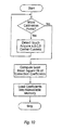
- the initial measurement procedure proceeds as follows. A loop is executed to sequentially detect touch as various positions on the substrate, until all values are obtained. After the required data is obtained, the least mean square fit of mapping coefficients is obtained. These coefficients are then stored in memory.
- a plurality of measured points are analyzed for determination of the algorithmic mapping.
- a number of measured points are obtained, e.g., ninety-nine points in a nine by eleven rectangular array, spaced one inch between centers on the sensor substrate surface, or for a quadrant-based system, 30 points per quadrant. More generally, the number of measured points is selected to be sufficient, on a population basis, to provide a suitable accuracy of the touchscreen.
- the change in standard deviation value which is a statistical measure used to verify the goodness of fit, per additional point, thus tends to diminish to within a desired range when sufficient data is obtained.
- ADC analog-to-digital converter
- the ADC is preceded by a multiplexer, which sequentially reads the voltage output of each corner electrode transconductance amplifier through a multiplexer 124, which is then passed to the processor 125.
- the processor computed the corrected position employing predetermined coefficients stored in an electrically programmable read only memory (EPROM), which is a nonvolatile memory.
- EPROM electrically programmable read only memory
- the nonvolatile memory 123 is associated with the sensor and provides data through a serial link to the processor. The position data may then be passed through a serial link to a host processor.
- mapping coefficients were computed using MathCad software from measurements obtained using the above method. This method is outlined below. It is noted that C programming language code executes more efficiently, and may be advantageously be employed.
- x ( b ⁇ 0 + b ⁇ 1 ⁇ A + b ⁇ 2 ⁇ B + b ⁇ 3 ⁇ C + b ⁇ 4 ⁇ D + b ⁇ 5 ⁇ A 2 + b ⁇ 6 ⁇ AB +
- One system according to the present invention applies a mapping algorithm having individualized mathematical coefficients, suitable for defining a mapping relation of all or a portion of the sensor system.
- the algorithm may include terms having differing magnitudes, and in fact, terms which are expected to have low absolute values over the entire range of inputs may be eliminated from consideration, thus simplifying evaluation of the mapping algorithm.
- the sensor active area i.e., the touch position sensitive portion, may be subdivided into regions, each associated with a different set of algorithmic mapping coefficients. For example, the sensor may be subdivided into quadrants, and the presence of the repositionable electrode within any given quadrant determined based on a simple pre-analysis of the corner electrode data to find the largest value. This regional localization allows application of a mapping relation including a set of coefficients optimized for that region.
- corner current-squared terms a5A 2 , a9B 2 a12C 2 and a14D 2 may be omitted (a5, b5, a9, b9, a12, b12, a14, and b14 each equal 0) for some screen designs , because these terms are expected to have low significance in the mapping algorithm, and evaluation thereof is not usually required to achieve a particular desired performance.
- This equation thus includes the zero order, first order and cross product terms, but not higher order terms.
- the characterization process for each sensor system involves recording the value of the electrical signals at each of the sensing electrodes, relative to a grid of physical positions on the substrate, each position on the grid being activated by a repositionable electrode, this electrode being the cover sheet activated by a stylus positioned by a highly accurate positioning device.
- the recorded values which are temporarily held in the test computer, are then used in a least squares curve fitting program in the test computer, selecting coefficients for a fit equation which seeks to minimize the sum of the squared error between the coordinate produced by the equation and the actual physical coordinate.
- a set of coordinate values for X and Y are given as the desired output from the model polynomial.
- the difference between the value of each actual point and the value given by the polynomial is squared.
- the object is to solve for the coefficients of the polynomial that produce the minimum error for a given data set (an array of current values from the sensing electrodes based on a grid of specific points on the touch screen). Solving for the coefficients involves partial differentiation of the squared error term with respect to each coefficient, setting each equation to zero to find the minimum error for that coefficient, then solving the resulting N simultaneous equations.
- the resulting coefficients are stored in a non-volatile memory which is part of the touchscreen assembly (alternatively they may be stored on a computer floppy disk to be loaded into the host computer of which the touchscreen ultimately becomes a part).
- the touch system will employ these coefficients to calculate a touch location directly from measured detector values.
- These detector values are used as variables A, B, C, and D in one equation each for X and for Y, similar to that shown above for Y, the coordinate output being accurate to within a desired limit without further corrections.
- the only values used to describe touchscreen characteristics are the derived coefficients.
- Original values from the test grid of physical locations are not employed following the curve fit process. Thus, in contrast to table-look-up correction schema, they are not a requirement. What is stored are coefficients of a mathematical function that directly maps the sensing electrode values into X and Y.
- the quadrant of a touch position is estimated based on the raw data input, and the appropriate algorithm applied. Accordingly, 11 equations are solved for 11 unknown coefficients for each axis, in each quadrant. In this case, one coefficient may be normalized, so that only 10 coefficients need be stored for each polynomial. The coefficients are then programmed into non-volatile memory associated with the digital signal processor.
- Figure 5 shows typical accuracies for X reported versus X actual for an example touchscreen according to the present invention. It is noted that the product terms of corner currents need be calculated only once for corresponding terms of the mapping algorithm for each respective axis, thereby simplifying calculation execution.
- the curve fit may be improved by using the above described technique with the addition of higher order terms, such as a third order term, e.g., BCD, to improve the curve fit.
- a third order term e.g., BCD
- the method according to the present invention applies a predetermined form of algorithm, with a set of coefficients which vary between examples of the sensor system based on an individual measurement step. Therefore, in such a system, each unit is assembled, and a predetermined initial measurement procedure performed to determine the values of information corresponding to the mapping relationship to be stored, including the application of a repositionable electrode or fixture to a plurality of positions while injecting a current signal, with the resulting electrical signal from the plurality of electrodes on the conductive surface measured. After the measurements are obtained, the measurement data is processed to produce a set of coefficients, which are stored in a memory in conjunction with the sensor system. For example, a coupled memory device as disclosed in U.S. 5,101,081 may be employed.
- mapping coefficients may also be provided separately from the sensor system, e.g., on a magnetic disk (floppy disk) or in a module. Therefore, the algorithmic processor for mapping the sensor system output need not be integral with the sensor system, and advantageously, the processor is a host executing both a mapping algorithm and application software.
- the processor controls the multiplexer to sequentially sample the values derived from the current passing through each corner electrode 160, digitize the voltage, and store these values in random access memory in the processor. The values are then pre-analyzed for detection of a touch 161, and if detected, processing continues to determine the position of the touch. The various products are calculated 162, and the quadrant in which the touch occurs identified 163. The processor then evaluates the mapping equation for both the X and Y axis 164, and outputs the X and Y coordinates in bit-serial manner through the serial data interface, generally complying with the RS-232 format at approximately 9600 baud.
- processing the signals from the electrodes optionally further processing may be conducted to reduce noise and possibly introduce a small zone of hysteresis.
- Further standard input processing techniques such as input debouncing, may also be implemented in conjunction with the present invention.
- the processor may optionally determine the impedance of the contact by determining the voltage imposed by the current source on the repositionable electrode, to determine whether the force or touch on the cover sheet is sufficient to allow the nominal current to pass, i.e., whether the current source is operating at a "rail" of the power supply.
- a threshold touch may be defined to avoid false touch indications.
- a type of self calibration may be employed, based on the baseline readings from the sensor system.
- the detector outputs during a "no touch" baseline period may be employed to extract out any baseline drift or interference.
- this compensation requires a system in which signals are superposed additively, or where the superposition effects are otherwise known.
- a conductive surface substrate 110 is provided essentially as in Example 1. However, as shown in Figure 6, no microcontroller is provided in conjunction with the sensor system. Instead, an analog data acquisition system 200 with an input multiplexer and serial interface is provided which sequentially polls the inputs and transmits the data in serial format through a serial interface driver 202 to a host processor 201, which evaluates the mapping algorithm from the raw data. Upon startup, the host processor 201 reads the contents of a coefficient storage nonvolatile memory 123, through the serial interface driver. After the stored data is transferred, the system then transmits the digitized data from the analog data acquisition system 200.
- the method according to the present invention is also applicable to capacitive touch position sensors.
- a constant current RMS AC signal is selectively injected through one of the fixed electrodes on the conductive surface, e.g., 200 ⁇ A sinusoidal RMS.
- the repositionable electrode includes a dielectric barrier material with an impedance to a reference, so that proximity to the conductive barrier contact attenuates the signal at that point, resulting in a variable current loss.
- the current at each of the other fixed electrodes is measured.
- the input current is therefore equal to the currents measured at the other corners plus the parasitic losses of the system.
- a constant current RMS AC signal is selectively transmitted from a touch position to a conductive surface.
- AC currents at the plurality of electrodes are measured using known techniques.
- a known capacitive sensor system includes an overlay sheet, having an insulating separator from a conductive substrate, disclosed in U.S. 4,623,757. This type of touch position sensors may also be generally compensated according to the present invention.
- a capacitive embodiment of the invention is accomplished by providing a source of alternating current to one corner of a resistively-coated substrate, and sensing the current flow at the remaining three corners, as shown in Fig. 8.
- a touch at any location on the surface of the substrate will result in a current being drawn from that location and because of the current flow relationships discussed in the resistive embodiment, there will be a set of currents at the three sensed corners that is unique to that touched location.
- a set of coefficients may be derived to allow mapping of the three sensing electrode transform these unique sets into a two-dimensional coordinate system.
- a substrate is provided generally as in Example 1. As shown in Figure 8, one corner of the substrate 210 is connected to an alternating current constant current source 250, having an output of 200 ⁇ A RMS. If DC coupled to the amplifiers, the input signal preferably has a negative voltage bias.
- the probe 251 is any dielectric with a ground path, e.g., a human finger.
- the three remaining corners of the substrate are connected to transconductance amplifiers 252.
- the output of the transconductance amplifiers 252 are then multiplexed and sequentially read by an analog to digital converter 255.
- the sensor system 256 is interfaced serially through a serial port interface 261 with the host 257.
- a nonvolatile memory 258 is associated with the sensor system, which includes stored mapping coefficients.
- the host system 256 Upon initialization, the host system 256 reads the stored mapping coefficients from the nonvolatile memory 258 through the serial port interface 261 and stores then in random access memory associated with the host computer 257. Thus, no microprocessor need be provided with the sensor system 256.
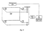
- a substrate 220 having a plurality of force detectors 221.
- the outputs of the detectors 221 are multiplexed through multiplexer 222 and digitized by analog to digital converter 223.
- a microcontroller 224 receives the output of the analog to digital converter 223, and determines a position of touch based on a mapping algorithm stored in ROM 226, based on a series of coefficients stored in nonvolatile memory 227 which are derived from an initial measurement procedure and least mean square fitting.
- the force against the substrate is divided between the detectors 221, with a nonlinear relationship between the touch position and the response of any detector 221.
- the output response of each detector 221 may also be nonlinear. Further, compliance of the substrate 220 may also produce nonlinearities.
- the algorithm corrects for the relationship of force location and detector 221 output to produce a corrected results.
- a substrate having a metallized pattern as shown in Fig. 12 is employed instead of the conductive surface substrate 110 according to the method of Example 1. While a linearization array such as shown in Fig. 4 may also be used, such a complex and space consuming array is not necessary.
- the metallized pattern includes an array of peripheral metallized elements 301, 302, 303, including corner electrodes 301 for making electrical connection to the substrate.
- the substrate is a glass sheet coated with ITO in known manner.
- the peripheral metallized pattern includes an interrupted linear array of deposited metal strips, each about 1 / 32 inch wide, and separated by about 0.25 inches.
- the substrate is rectangular, with a length of about 12 inches and a width of about 10 inches.
- five strips 301, 302 are provided, two terminal strips 301 of approximately 0.75 inches, and three central strips 302 of about 1.5 inches each.
- the terminal strips 301 of the array along the length are provided with a patch suitable for connection of external wires.
- three metallized strips 303 are provided, each about 1.25 inches long. The metallized pattern reduces spatial variations in current density through the substrate, reducing the complexity of model-based compensation of the corner current outputs for a given accuracy output.
Landscapes
- Engineering & Computer Science (AREA)
- General Engineering & Computer Science (AREA)
- Theoretical Computer Science (AREA)
- Physics & Mathematics (AREA)
- General Physics & Mathematics (AREA)
- Human Computer Interaction (AREA)
- Measurement Of Length, Angles, Or The Like Using Electric Or Magnetic Means (AREA)
- Position Input By Displaying (AREA)
- Switches That Are Operated By Magnetic Or Electric Fields (AREA)
- Arrangements For Transmission Of Measured Signals (AREA)
- Electronic Switches (AREA)
- User Interface Of Digital Computer (AREA)
Abstract
Description
- The present invention relates to a method for relating a plurality of input values with coordinate positions (164) of a medium having a surface (110), the input values being responsive to and varying in corresponding relationship to a coordinate position of the surface over a range of coordinate positions.
- The functionality of a touchscreen system (typically including a touchscreen and an electronic controller) requires that there exist a relationship between the physical location of a touch, e.g. by a person's finger, and some coordinate schema. In general, the coordinate system of choice is a two-dimensional Cartesian system with orthogonal horizontal (X) and vertical (Y) axes. The system accuracy is defined as the error between the physical location of the touch and the location reported by the touchscreen/controller. Typically, system accuracy is expressed as a percentage of the touchscreen dimensions.
- A touchscreen system may be considered to have two classes of error, (i) those resulting from the design and implementation of the coordinate transformation method (systematic error), and (ii) those resulting from random unit to unit errors within a given class of sensors (manufacturing variance).
- Known conductive touchscreen systems have a transparent substrate with a conductive film, e.g., indium tin oxide (ITO) deposited thereon, which is subject to variation in surface conductivity, i.e., ±5% or ±10%. A particular additional source of errors in systems employing such substrates is the non-linear variation in sensed probe injection current inherent in the configuration of a generally rectangular substrate with electrodes at the corners. This results in a non-uniform current density at various portions of the substrate, especially near the electrodes. Because of the gross non-linearities, it is generally considered undesirable to attempt to perform a piecewise linear compensation, i.e., directly compensate for repositionable electrode position based on a lookup table calibration procedure. Prior methods have therefore sought to include physical linearization structures, such as complex current injection electrodes, in order to reduce the non-uniformity in surface current density, and to linearize the potentials on the substrate. These complex linearizing structures often include complex conductive patterns, diodes or transistors to redistribute or control the redistribution of currents. Still other methods have sought to apply a mathematical algorithm to compensate for the expected distortions duc to the rectangular physical configuration.
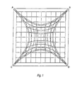
- The coordinate transformation methods employed in prior systems may be categorized into two basic technologies, herein called electromechanical and modeling, each based on a ratiometric approach, whereby there is an assumed mathematical relationship between measured data and a physical location on the surface of the sensor. Typical distortion of the coordinate values in X and Y of an uncompensated rectangular conductive substrate is shown in Figure 1.
- Lookup tables provide an addressable storage for correction coefficients, and have been proposed for use in correcting the output of touch position sensors based on a number of technologies. These systems receive an address, i.e., a pair of X and Y values, which corresponds to an uncorrected coordinate, and output data which is used to compensate for an expected error and produce a corrected coordinate, generally in the same coordinate space as the uncorrected coordinate. Proposals for such schemes range from zero order to polynomial corrections. See, U.S. Patent No. 4,678,869. In general, the uncorrected coordinate input to the proposed lookup table is initially linearized, i.e., by physical means or by algorithmic means, as discussed below, so that the lookup table operates in a linearized space. Lookup table data values derived from a calibration procedure thus directly correspond to the calibration data coordinate values, and define calibration regions.
- There is a class of systematic error compensating methods comprising electromechanical modifications to the touchscreen system, seeking to approximate an orthogonal grid of electrical potentials from the characteristics shown in Figure 1. There are four basic methods (summarized below) in this category. The design of such electromechanical methods addresses the systematic error, described above, for a given class of touchscreen. The nature of these methods often results in a significant current drain on the system and the multiplicity of electrodes and/or resistance patterns leads to a high sensor cost. Further, the management of the corrective methods, e.g. excitation switching, sensing plane selection, electrode selection, etc., mandates an interactive control mechanism that adds to the system cost. To correct unacceptable errors occasioned by manufacturing variances within the given class of touchscreens, additional error correcting methods, such as table lookup, may be employed for each individual touchscreen.
- This, the most elementary form of correcting the fundamental distortion characteristics is by creating highly
conductive bus bars 3 on opposing axes of the substrate I (Figure 2). Excitation is applied to the bus bars 4 and a conductive coversheet 2 provides for the relocatable electrode. Measurement is made as if the touchscreen were a potentiometer, the position of the "wiper" being the location of the touch, in that plane of excitation. The excitation is then switched to a second set of bus bars in an orthogonal plane (in some cases located on the cover sheet 2) to define the second coordinate. This technique is exemplified by U.S. Patent No. 3,622,105. The principal drawback to this technology is its current drain. Further, in those cases where the cover sheet is employed for the second excitation plane, any coversheet damage will result in positional location errors. - US 5,412,161 and US 5,115,107 disclose a segmented touch position sensor which corrects for scale and offset, but not skew or distortion. Segments are defined by bus bars and appropriate orthogonal excitation patterns. A unidimensional correction equation is provided for each axis within each segment.
- EP 0,571,226 discloses a touch position sensor employing a fine array of conductive lines disposed at right angles of a display. The position of a touch is determined by sensing a capacitance on each line, and representing the sequential capacitance values in a histogram. The position is statistically determined along each axis, and corrected for propagation delay, inward displacement, waveform, and periodical fluctuation.
- Multi-feed technology, typified by U.S. Patent No. 5,438,168, employs active control of
multiple electrodes 10 located around the periphery of theresistive substrate 11, as shown in Figure 3. The operation of these systems are generally functionally equivalent to that of bus-bar technology, in that linear voltage gradients are generated for sampling by a cover sheet relocatable position sensor. Since allelectrodes 10 are located on onesubstrate 11, it is unaffected by cover sheet damage. However, it is a high current drain system, and requires a large number of interconnections. Failure or degradation of any of itsswitching elements 12 results in system errors. - Many known of corrective methods include use of
resistive patterns 21 on, or external to, thetouchscreen 20, in such a sequence that the resistive gradient of thetouchscreen 20 is approximately the same across its surface, as shown in Figure 4. U.S. Patent Nos. 3,798,370, 4,293,734, and 4,661,655 typify this technique. These systems have the high current consumption associated with electromechanical methods, and, because of the complexity of theresistive patterns 21, are prone to errors resulting from manufacturing variances. - A second category of coordinate generation technique is based on mathematical functions, chosen because of assumed mathematical relationships for a given class of touchscreens. These methods result in X and Y values that require further adjustments or corrections either because of inadequacies in the assumptions or because of manufacturing variations, or both.
- One method, described in U.S. Patent No. 4,631,355 and Federico et al., "17.2: Current Distribution Electrograph" SID 86 Digest, p. 307, relies on an a priori assumption concerning the mathematical distribution for points on a touchscreen. Each plane is extracted by ratiometric methods, and the axial "astigmatism" of each plane, as exemplified in Figure 1, is then linearized by the use of a second order polynomial equation whose coefficients are empirically derived. U.S. Patent No. 4,631,355 notes that manufacturing variation errors on the order of 5% are usual, but does not compensate for them, and therefore would need to be corrected for by additional techniques in order to provide an accurate touch position sensing method. Therefore, Federico et al., "17.2: Current Distribution Electrograph" SID 86 Digest. proposes storing calibration data in a lookup table, for operation separately from the algorithmic compensation system and as a subsequent step to correct the sensor output.
- U.S. Patent No. 4,806,709 is predicated on the assumption of a linear relationship between signals at an electrode located on the conductive surface and the distance between that electrode and the touch location. Using this assumption, the signal from each electrode is employed in an equation that describes the arc of a circle with its origin at the electrode, with a second equation that defines the touch location as the intersection of two or more of such arcs. An implementation of such an approach would have two principal sources of error, (a) non-linearities in the assumed signal/distance relationship, measured data confirming such non-linearities, and/or manufacturing variances which would lead to an error in the calculation of each arc radius, and (b) the classic problem of positional error caused by the difficulty in resolving the angles of intercept as the arcs approach tangency.
- It is an object of the present invention to find a method for providing an accurately determined coordinate position of a physical effect on a medium.
- This object is achieved by a method according to
claim 1. - The present invention provides a method for providing an accurately determined coordinate position of a physical effect on a medium with a plurality of sensors, each detecting the effect through the medium. The plurality of sensors are mapped to the output coordinate system through a mapping relation, which requires no predetermined relationship of the sensed effects and the coordinate system. The form of the mapping relation is an equation, i.e., a polynomial consisting of various terms, with the coefficients of the mapping equation determined for each example of the integrated sensor, to account for individual manufacturing variations as well as the systematic relationship of the detectors to the coordinate output.
- In a preferred embodiment, a touchscreen is provided, having a conductive rectangular substrate with electrodes at each corner of the substrate. An electrical field is induced or effected by proximity of an element, and the electrical field is measured by the plurality of electrodes. Generally, due to the conductive nature of the substrate, a current distribution between the detectors will be measured, the distribution varying with a position of the element with respect to the substrate. Thus, for each position of the element, a unique set of detector outputs will be obtained. A mapping equation is evaluated to map the detector outputs to a desired position coordinate system. Generally, the desired position coordinate system is a Cartesian coordinate system, although other mappings may be provided.
- During a manufacturing procedure, each sensor substrate is individually mapped, using a plurality of test points. These test points need not have any particular positions with respect to the substrate, although a relatively large number are preferably provided, dispersed across the surface of the substrate, or at least that portion which is expected to be used. The physical position of each test point is accurately recorded, along with the detector outputs at that test point. A mapping equation is then defined, based on the recorded data, which optimizes an error of the output coordinate positions with respect to the detector outputs. For example, a least mean square curve fitting may be employed to determine a plurality of coefficients of an equation.
- A particular characteristic of the present invention is that, without need for physical or algorithmic prelinearization, the mapping equation is capable of producing accurate coordinate position output from the detector outputs in a single expression. Therefore, the data stored in memory is not in the form of an addressable error lookup table, but rather of the form of data describing a mapping for a set of sensor data coordinates to touch coordinates, without any presumed linear relationship.
- According to a preferred embodiment, a conductive touchscreen is provided which measures the effect of a touch position on a plurality of electrodes to determine a position of the touch. The touch may inject a current, e.g., in a resistive touchscreen, or perturb an electrical field, e.g., a capacitive touchscreen. In most applications, a rectangular substrate having four corner electrodes is provided, although other shapes and electrode arrangements are possible.
- In another embodiment, the physical effect is a localized force applied to a stiff, or force transmissive element. The element is suspended by a plurality of force detectors, which may be resistive, piezoelectric, inductive, optical, acoustic, or employ other known sensor types. The outputs of the force transducer detectors are mapped to a coordinate location of the force application. This mapping accounts for flexion of the element, configuration of the element, force distribution at the detector locations, and manufacturing variation in the element and detectors.
- In principal, therefore, the medium conducts a physical effect, which is sensed at a plurality of sensing locations. In many instances, there will be a monotonic relation of distance from the location of the effect to each detector and the detector output, although this is not required. However, it is generally required that each set of detector outputs uniquely correspond to a location. Further, it is preferable that there be a continuous first derivative of the detector responses with respect to location of the effect, allowing a continuous mapping function to be employed. The physical effect need not be electrical or force, and may be magnetic, vibrational or acoustic, or another type of effect.
- The present invention does not rely on a presumption of ratiometric sensing of effects.
- A number of proposed methods rely on uniformity of a conductive media, to detect an amplitude, distribution or delay of a signal, and are thus subject to errors directly resulting from a failure to meet this criteria. Therefore, according to one aspect of the invention, empirically observed data for the media and system incorporating the media is obtained, in order to define an actual mapping relation of the detector outputs and the location of the effect. This data may be processed to various levels. Preferably, an efficient model is employed, with a limited number of stored coefficients of a polynomial curve-fitting equation. The coefficients are preferably derived by a least mean squares fit. The specific terms used in the polynomial equation may be selected based on a sensitivity analysis, preferably with only terms necessary to achieve a given accuracy employed. In general, because the system is a mapping system rather than a linearization followed by calibration system, the stored coefficients do not individually correspond to regions, locations or coordinates of the medium.
- One method of limiting the mapping evaluation equation complexity is to define a number of regions of the media, each region being associated with a set of coefficients. In use, the region of the physical effect is estimated, and the set of coefficients corresponding to the estimated region employed to map the detector outputs to the location of the effect. Therefore, while increased coefficient storage is necessary, the complexity of the mapping relation may be reduced and/or the resulting accuracy increased. In general, the estimation of the region will be a simple mapping of boundary regions based on comparisons of detector output data, and therefore there is no need to define an estimated coordinate position of the location of the effect. Typically, four regions are defined for a rectangular substrate medium, each region corresponding to an area around a corner electrode. In the case of the four regions, or quadrants, the region is determined simply by determining the detector with the largest output signal.
- In accordance with the present invention, nonlinearities such as the hyperbolic current distribution distortion of a conductive rectangular substrate with corner electrodes, or nonlinearities of substrates having a rectangular or non-rectangular shape with cylindrical, conic, spherical, ellipsoidal or other curvature or non-planar regions may be corrected to map detector outputs to a coordinate location of a touch. Further, in the same mapping process, manufacturing variations such as surface conductivity variations, electrode configuration variations, cover sheet variations, and the like, may also be corrected. Other aspects of the disturbance may also be measured. The mapping relation thus may compensate, in a unified system, for:
- (a) The configuration and properties of the medium;
- (b) The number, location and characteristics of each of the detectors;
- (c) manufacturing variations of the medium and detectors, and other portions of the system.
- The present method applies a mapping relation, determined individually for each sensor system, to correct for both nonlinearities and manufacturing variations to provide a high accuracy location coordinate output. Errors due to manufacturing variations such as non-uniform coating thickness, bubbles or scratches in the coating, differences in the connection resistance of the cover sheet or the fixed sensing electrodes, or variations in the characteristics of the interface electronics are included within the mapping relation.
- According to the present method, a mapping relation is determined based on a plurality of empirical measurements, which compensate for the overall and actual properties of the sensor system. Further, the generation of the coefficients for the mapping algorithm may performed internally to the controller or on an external system.
- Measurement points must generally be spaced less than one half of the spatial Nyquist frequency of significant variations, and these variations must be actually measured. According to one embodiment of the invention, the mapping algorithm may be implemented to compensate for variations which are actually present, without further complexity. Therefore, it is possible to uniquely define the mapping characteristics of an individual sensor system for the required degree of accuracy, and apply an algorithm having the least necessary complexity. For example, where a particular manufacturing variation occurs in one quadrant of a sensor system, a mapping equation applied for that quadrant may have greater complexity than other quadrants. The format of the mapping equation may stored explicitly or implicitly in the stored data.
- Because essentially complete mapping may be achieved through application of the algorithm, the present system does not require physical means for controlling the current distributions through the conductive surface, thus allowing a simple substrate configuration with a plurality of corner electrodes, e.g., four corner electrodes of a rectangular panel, to receive electrical signals. The electrical signals, it is noted, may be of constant current, e.g., a DC signal, or of time-varying current waveform having a constant RMS value, e.g., an AC signal. Advantageously, the corner electrodes need not be sequenced or subject to complex time domain analysis; therefore, a simple current source and transconductance amplifiers may be provided. The present method according to the present invention may be used in both resistive and capacitive sensing systems. The present method also allows superposition of different sensing systems, e.g., static and dynamic signals may be simultaneously measured.
- Advantageously, the set of mapping relation coefficients are efficiently stored. Further, the scheme of the present method does not assume a ratiometric relationship of the physical effect and the detector outputs, allowing high performance even with non-uniform and non-linear systems.
- The computing load associated with typical position determining equations consists of 26 multiply and 20 addition operations to compute both X and Y coordinates, a load well within the capabilities of typical low-cost processors, such as Intel 8051 and derivatives thereof to process within a suitable time-frame. In fact, the method according to the present invention generally has no requirement for any bi-directional interaction between the touchscreen and the remainder of the system, to accomplish the transformation of sensed signals to location coordinates, thus permitting a low-cost embodiment in which the conventional touchscreen controller may be eliminated, the execution of the algorithms being performed by the host computer that also contains the associated application programs. Host processors in systems commonly interfaced with touchscreen sensors, such as Microsoft Windows compatible computers, have sufficient available processing power to evaluate a mapping relation of a touchscreen sensor and execute application programs, without substantial degradation in performance.
- The mapping relation information may be stored in a memory device physically associated with the sensor system, or in a separated memory that is used in conjunction with the system. The relatively small number of coefficients necessary allows use of a small memory device, and since the coefficients may be transferred to a local storage of a processor on device initialization, the speed of the memory is not critical. Advantageously, a serial interface EEPROM, physically associated with the interface electronics of a touchscreen with a host processor is employed to store the coefficients. Other memory devices include rotating magnetic media, e.g., floppy disks and the like, and semiconductor memories. While not preferred, it is noted that creation of the mapping equation may be performed subsequent to the manufacturing process, e.g., following device installation on a host system.
- While a generic polynomial may be defined which includes one coefficient for each data point, it is preferred to define a simpler equation, having fewer coefficients, and then optimize the coefficients of the simpler equation based on the available data to optimize the error. It is noted that the lowest mean square error is but one optimization technique, and one skilled in the art may optimize differently, if desired.
- Where a term of the mapping algorithm equation is found during the design phase of the sensor to have low significance for the entire range of mapping, it may be ignored. Thus, in an embodiment where the sensor system is divided into quadrants, higher order terms may be selectively evaluated or ignored. Thus, where the mapping space is subdivided, terms with low expected significance in any region of the space may be ignored for that region, allowing reduced processing to produce a corrected output while maintaining accuracy
- Therefore, one aspect of the present invention provides algorithmic mapping of electrode inputs based on relocatable probe position by means of a mapping formula or set of formulas, derived from an individualized measurement procedure.
- In one embodiment, a mapping region defined by the algorithm is not coincident with, and larger than a measurement region, defined by a particular measured point and the arrangement of the other measured points. It is noted that the mapping relation for each coordinate axis need not be of the same form, especially where the substrate is asymmetric.
- In addition to its simplicity and low manufacturing costs, the power requirements for this touchscreen system are minimal, some three orders of magnitude less than conventional resistive touchscreens, thus facilitating its application in battery powered systems.
- The various modeling or algorithmic and electromechanical linearization techniques may advantageously combined to reduce the complexity of either implementation. Therefore, while it is preferred that the various compensation schemes seek to linearize the output representation, a more general statement of the invention is that the electromechanical technique produce output signals which require a reduced complexity algorithm to linearize.
- One particular advantage of the combination of a modeling technique and an electromechanical technique is that the electromechanical technique may be implemented during the same fabrication step as the forming of the conductive pads for the sensing electronics of a resistive or capacitive touchscreen. Thus, the process is nearly identical in complexity and therefore price. However, the resultant signals produced by the system may be perturbed in such a way that various higher order terms become insignificant, or conversely, the achievable accuracy is increased for the same complexity calculations. Therefore, the memory requirements for storing the correction coefficients are reduced and the computing resources for performing the calculations are reduced. These become important considerations where, for example, the host processor performs the corrections on a real-time basis, as might be provided in a personal digital assistant or other integrated touchscreen system.
- The linearization pattern may include, for example, a set of interrupted lines near the periphery of the substrate. These interrupted conductors tend to redistribute the equipotential lines, as shown in Fig. 1, away from the centroid and toward the edges of the substrate. Therefore, the sensitivity of the system is equalized over its surface, while the output is made more linear and less parabolic.
- In a like manner, the output of the touchscreen may be subjected to an analog or digital electronic prelinearization step, in which the output signals are preprocessed to reduce the required calculational complexity necessary for producing coordinate outputs. In this case, the accuracy of the prelinarization system need not be high, so long as it is repeatable or other influences, such as temperature, are accounted for. For example, temperature may be an input into the curve fitting compensation system. This, in turn, might allow use of a low cost and/or complexity prelinarization circuit, for example CMOS logic cell circuits driven in analog mode.
- As stated above, the method according to the present invention is not limited to electrical sensing methods.
- The preferred embodiments of the invention will be shown by way of drawings of the Figures, in which:
- Fig. 1 of the prior art shows a map of X and Y coordinates resulting from an assumption of a ratiometric relationship on an uncorrected surface;
- Fig. 2 of the prior art shows a bus bar system, generating a relatively linear gradient as you move from one to the other on application of a voltage potential between bus bars on either axis;
- Fig. 3 of the prior art shows a multi-element system, employing a quasi bus bar method, wherein a reasonable linear gradient is produced by switching a voltage across one axis while holding the other off, switching sequentially between the selected electrodes;
- Fig. 4 of the prior art shows a resistive network, wherein the edges of the substrate have the same resistive characteristics as the center of the screen;
- Fig. 5 of the present invention is a graphical representation of accuracy with the substrate divided into quadrants;
- Fig. 6 of the present invention is a simplified block diagram of a touch screen sensor employing a host computer to compensate the output;
- Fig. 7 of the present invention is a flow chart of a method of mapping the sensor according to Fig. 6;
- Fig. 8 of the present invention is a capacitive embodiment, in which source excitation is provided as AC current fed to one corner, with a current flow at the remaining 3 current detectors monitored for the effects of a dielectric;
- Fig. 9 is a block diagram of an alternate controller for a touchscreen as shown in Fig. 6;
- Fig. 10 is a flow diagram of a measurement procedure according to the present invention;
- Fig. 11 is a semischematic view of an algorithmically compensated pressure and position sensor; and
- Fig. 12 is a top view of a metallization pattern at the periphery of a conductive touchscreen.
- The detailed preferred embodiments of the invention will now be described with respect to the drawings. Like features of the drawings are indicated with the same reference numerals.
- The method according to the present invention applies a mapping relation, i.e. an algorithm including a polynomial equation, which efficiently maps the input values from the detectors to a coordinate scheme, with the required degree of accuracy. In fact, it has been found by the present inventors that the number of polynomial coefficients required for a desired performance, e.g., 1% of full scale accuracy, is significantly less than the number of measured points required to derive these coefficients.
- For typical ITO coated glass substrates used for resistive touch position detectors, this results in efficient polynomial coefficient storage. This system, in principal, has broad application where a mapping is desired between a plurality of detector outputs relating to a physical disturbance and a coordinate system position of the physical disturbance.
- Where the sensor system includes a dedicated controller, the algorithmic mapping system controller is preferably implemented as a single chip microcontroller which also serves as the communication controller for the fouchscreen device, outputting coordinates to the host computer system over, e.g., a serial communication port. In addition, it is preferred that the processing overhead for the mapping relation be small enough to allow use of simple, low cost, low power microcontrollers, such as the Intel 80C51 and various known derivatives, and application specific integrated circuits incorporating an 80C51 core device. Advantageously, the microcontroller includes an analog-to-digital converter (ADC) having at least 10 bits of resolution, although separate ADCs having 12-16 bits may also be used. The mapping data according to the present invention is stored in a memory, which is preferably physically associated with the touchscreen. For example, a serial-output electrically programmable read only memory (EEPROM) may be physically included in the housing or attached cable of the sensor, for storing the coefficients. Another example is an EEPROM included in, or associated with, a single chip microcontroller.
- The mapping method according to the present invention may also be provided as a software driver in a connected host processor. In this case, it is necessary to communicate to the host processor the algorithmic coefficients for mapping of the sensor panel. The host system may be, e.g., a computer system running Macintosh System 7, UNIX, or Windows.
- The present method provides a plurality of detectors as inputs to the mapping equation. More preferably, each detector is located at a corner of a rectangular substrate.
- As part of the production process of a sensor system, a measured data set is obtained for each touch screen to obtain a set of detector outputs at determined locations. Preferably, these points are in a grid, and more preferably in a predetermined array. However, so long as the physical positions of physical effect are accurately known, there is no requirement that the set of points be the same for each sensor system. A computer program then solves the later explained N simultaneous equations to find the polynomial coefficients of a mapping equation for that specific touch screen, then stores them into a non-volatile memory device which is preferably an integral part of the touch screen assembly. During use, when the touchscreen is connected to its computer (either a dedicated computer within a separate controller or the host computer associated with the touch system) the computer upon system initialization will read the non-volatile memory, retrieving the coefficients for that particular screen and storing them in its local memory, subsequently employing them to derive a touch location from measured current data. Each screen is thus individually characterized so that unit to unit variations are individually corrected. Ultimate accuracy is only dependent on the hardware and complexity of the chosen model. Therefore, the present invention allows a range of mapping complexity to be implemented.
- As shown in Figure 9, a
sensor substrate 110 consisting of an indium-tin oxide (ITO) coating with an average resistivity of 38,45 ohms/cm2 on an approximately 25,4cm by 31,75 cm soda-lime glass substrate, having on each corner a 1,27 cm x 1,27 cm coating of silver frit is provided. Manufacturing tolerance of the resistivity of the ITO coating is about ±10%, and thus there may be significant surface variations. Electrical connections in each corner of the substrate were approximately 0,635cm x 0,635 cm and located 0,635 cm from each edge. Thetouch probe 116 was connected to a -200 µA constantcurrent source 121 with a small (about 0,813 cm) ball tipped metal stylus, which was pressed directly against the ITO surface. For calibration of measurement positions, touch location was defined by a checking grid made from 0,157 cm ABS plastic having ninety nine, 0,157 cm holes drilled on 2,54 cm centers, 11 columns for X and 9 rows for Y. - Because the system incorporates a constant current driver, the resistivity of the coating is not a factor in the design of the sensor, thus enabling the most cost-effective coating to be selected.
- The sensor device is interfaced with a circuit for measuring an electrical signal through each of the possible paths from the repositionable probe to the fixed electrodes. For example, a constant current is injected, i.e., sourced or sunk, through the repositionable probe, and the fixed electrodes are clamped at ground potential (or an arbitrary reference potential with respect to ground), with the respective currents measured. Alternatively, a current may be presented between the repositionable electrode and each fixed electrode, with the respective impedances measured.
- The electrical connections were formed silver frit contact, although other suitable stable electrical contact systems may be employed. Each corner electrode is held at a virtual ground by an operational amplifier configured as a
transconductance amplifier 120, such as an National Semiconductor LF347N, and the respective currents converted to voltage signals. The use of transconductance amplifiers allows high gain and low sense current operation, and avoids the distortions which are generally introduced by sense resistors, and high currents which may damage certain coatings, such as nickel-gold. Other types of current measurement techniques are known, and may be employed. The transconductance amplifiers employed in the present system are inverting, and therefore the repositionable electrode sinks current rather than sources it to provide a positive output from the amplifier. - During the initial measurement procedure to determine the mapping relationship to be employed by the sensor system, i.e., to define the values of information to be stored in the memory associated with the sensor system, as shown in Fig. 10, the output of the analog-to-digital converter is ported by the microprocessor through the serial port on the board, without algorithmic processing. Thus, an external system obtained the detector output values, which were recorded in conjunction with actual measurement characterization conditions.
- The initial measurement procedure proceeds as follows. A loop is executed to sequentially detect touch as various positions on the substrate, until all values are obtained. After the required data is obtained, the least mean square fit of mapping coefficients is obtained. These coefficients are then stored in memory.
- According to the present invention, a plurality of measured points are analyzed for determination of the algorithmic mapping. Preferably, a number of measured points are obtained, e.g., ninety-nine points in a nine by eleven rectangular array, spaced one inch between centers on the sensor substrate surface, or for a quadrant-based system, 30 points per quadrant. More generally, the number of measured points is selected to be sufficient, on a population basis, to provide a suitable accuracy of the touchscreen. The change in standard deviation value, which is a statistical measure used to verify the goodness of fit, per additional point, thus tends to diminish to within a desired range when sufficient data is obtained.
- These signals were input to a microcomputer system having a 12-bit analog-to-digital converter (ADC) with four inputs. The ADC is preceded by a multiplexer, which sequentially reads the voltage output of each corner electrode transconductance amplifier through a multiplexer 124, which is then passed to the
processor 125. When the four corner current values were determined, the processor computed the corrected position employing predetermined coefficients stored in an electrically programmable read only memory (EPROM), which is a nonvolatile memory. In another embodiment, thenonvolatile memory 123 is associated with the sensor and provides data through a serial link to the processor. The position data may then be passed through a serial link to a host processor. - The mapping coefficients were computed using MathCad software from measurements obtained using the above method. This method is outlined below. It is noted that C programming language code executes more efficiently, and may be advantageously be employed.
- The current flowing into the substrate from the relocatable injection electrode is collected as the sum of the currents at each of the four sensing electrodes. Then, with the sum of the four currents being equal to a constant, i.e. A + B + C + D = constant, there exists a unique set of individual corner currents for each location on the touchscreen surface where the current is injected, which set includes any manufacturing variances for that specific touchscreen assembly.
- A general mapping polynomial expression is employed that directly transforms these four corner currents into physical X and Y coordinates for that specific sensor, in the general form of :


wherein A, B, C and D are the respective corner currents, al...al4 and bl...bl4 are the derived coefficients, and x and y are the coordinate positions. - One system according to the present invention applies a mapping algorithm having individualized mathematical coefficients, suitable for defining a mapping relation of all or a portion of the sensor system. The algorithm may include terms having differing magnitudes, and in fact, terms which are expected to have low absolute values over the entire range of inputs may be eliminated from consideration, thus simplifying evaluation of the mapping algorithm. The sensor active area, i.e., the touch position sensitive portion, may be subdivided into regions, each associated with a different set of algorithmic mapping coefficients. For example, the sensor may be subdivided into quadrants, and the presence of the repositionable electrode within any given quadrant determined based on a simple pre-analysis of the corner electrode data to find the largest value. This regional localization allows application of a mapping relation including a set of coefficients optimized for that region.
- Thus, the corner current-squared terms, a5A2, a9B2 a12C2 and a14D2 may be omitted (a5, b5, a9, b9, a12, b12, a14, and b14 each equal 0) for some screen designs , because these terms are expected to have low significance in the mapping algorithm, and evaluation thereof is not usually required to achieve a particular desired performance. This equation thus includes the zero order, first order and cross product terms, but not higher order terms.
- The characterization process for each sensor system involves recording the value of the electrical signals at each of the sensing electrodes, relative to a grid of physical positions on the substrate, each position on the grid being activated by a repositionable electrode, this electrode being the cover sheet activated by a stylus positioned by a highly accurate positioning device. The recorded values, which are temporarily held in the test computer, are then used in a least squares curve fitting program in the test computer, selecting coefficients for a fit equation which seeks to minimize the sum of the squared error between the coordinate produced by the equation and the actual physical coordinate.
- A set of coordinate values for X and Y are given as the desired output from the model polynomial. The difference between the value of each actual point and the value given by the polynomial is squared. To illustrate, the simplified equation for the squared error in Y is in the form:

where
- Differentiating with respect to, and solving for each coefficient in turn leads to a set of 15 equations for each coefficient respectively of each axis. An example of the above mentioned partial differentiation of the error term with respect to coefficient a5 is:

- The error is then set to zero to find the minimum for each coefficient as follows:
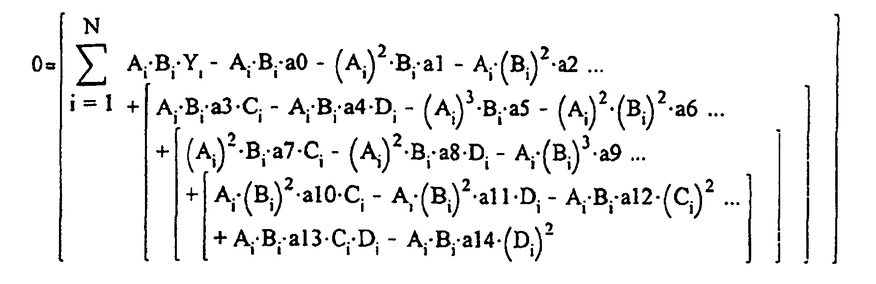
- Thus allowing solution of 15 equations for 15 unknown coefficients for each axis. Similarly, the least mean square fit coefficients for other equations may be determined and applied to produce the sensor system output.
- The resulting coefficients are stored in a non-volatile memory which is part of the touchscreen assembly (alternatively they may be stored on a computer floppy disk to be loaded into the host computer of which the touchscreen ultimately becomes a part). During use, the touch system will employ these coefficients to calculate a touch location directly from measured detector values. These detector values are used as variables A, B, C, and D in one equation each for X and for Y, similar to that shown above for Y, the coordinate output being accurate to within a desired limit without further corrections. The only values used to describe touchscreen characteristics are the derived coefficients. Original values from the test grid of physical locations are not employed following the curve fit process. Thus, in contrast to table-look-up correction schema, they are not a requirement. What is stored are coefficients of a mathematical function that directly maps the sensing electrode values into X and Y.
- In a further embodiment, the quadrant of a touch position is estimated based on the raw data input, and the appropriate algorithm applied. Accordingly, 11 equations are solved for 11 unknown coefficients for each axis, in each quadrant. In this case, one coefficient may be normalized, so that only 10 coefficients need be stored for each polynomial. The coefficients are then programmed into non-volatile memory associated with the digital signal processor.
- Using this quadrant approach, accuracies on the order of one percent of full scale were readily achieved. Figure 5 shows typical accuracies for X reported versus X actual for an example touchscreen according to the present invention. It is noted that the product terms of corner currents need be calculated only once for corresponding terms of the mapping algorithm for each respective axis, thereby simplifying calculation execution.
- The curve fit may be improved by using the above described technique with the addition of higher order terms, such as a third order term, e.g., BCD, to improve the curve fit. See Appendices to U.S. Patent 5 940 065.
- Using the present method, 10 coefficients are required for each of X and Y in each of the four quadrants, therefore requiring storage for 80 coefficients. These coefficients are calculated and applied with 16 bit precision, and will fit in a 2 Kbit memory device, e.g., a 93C56A EEPROM, to achieve about 2% full scale accuracy.
- According to a preferred embodiment, the method according to the present invention applies a predetermined form of algorithm, with a set of coefficients which vary between examples of the sensor system based on an individual measurement step. Therefore, in such a system, each unit is assembled, and a predetermined initial measurement procedure performed to determine the values of information corresponding to the mapping relationship to be stored, including the application of a repositionable electrode or fixture to a plurality of positions while injecting a current signal, with the resulting electrical signal from the plurality of electrodes on the conductive surface measured. After the measurements are obtained, the measurement data is processed to produce a set of coefficients, which are stored in a memory in conjunction with the sensor system. For example, a coupled memory device as disclosed in U.S. 5,101,081 may be employed. Of course, other arrangements may be used. The mapping coefficients may also be provided separately from the sensor system, e.g., on a magnetic disk (floppy disk) or in a module. Therefore, the algorithmic processor for mapping the sensor system output need not be integral with the sensor system, and advantageously, the processor is a host executing both a mapping algorithm and application software.
- During operation, as shown in Figure 7, the processor controls the multiplexer to sequentially sample the values derived from the current passing through each
corner electrode 160, digitize the voltage, and store these values in random access memory in the processor. The values are then pre-analyzed for detection of atouch 161, and if detected, processing continues to determine the position of the touch. The various products are calculated 162, and the quadrant in which the touch occurs identified 163. The processor then evaluates the mapping equation for both the X andY axis 164, and outputs the X and Y coordinates in bit-serial manner through the serial data interface, generally complying with the RS-232 format at approximately 9600 baud. - In processing the signals from the electrodes, optionally further processing may be conducted to reduce noise and possibly introduce a small zone of hysteresis. Further standard input processing techniques, such as input debouncing, may also be implemented in conjunction with the present invention.
- The processor may optionally determine the impedance of the contact by determining the voltage imposed by the current source on the repositionable electrode, to determine whether the force or touch on the cover sheet is sufficient to allow the nominal current to pass, i.e., whether the current source is operating at a "rail" of the power supply. Thus, a threshold touch may be defined to avoid false touch indications.
- A type of self calibration may be employed, based on the baseline readings from the sensor system. Thus, the detector outputs during a "no touch" baseline period may be employed to extract out any baseline drift or interference. In general, this compensation requires a system in which signals are superposed additively, or where the superposition effects are otherwise known.
- A
conductive surface substrate 110 is provided essentially as in Example 1. However, as shown in Figure 6, no microcontroller is provided in conjunction with the sensor system. Instead, an analogdata acquisition system 200 with an input multiplexer and serial interface is provided which sequentially polls the inputs and transmits the data in serial format through aserial interface driver 202 to ahost processor 201, which evaluates the mapping algorithm from the raw data. Upon startup, thehost processor 201 reads the contents of a coefficient storagenonvolatile memory 123, through the serial interface driver. After the stored data is transferred, the system then transmits the digitized data from the analogdata acquisition system 200. - The method according to the present invention is also applicable to capacitive touch position sensors. In this case, a constant current RMS AC signal is selectively injected through one of the fixed electrodes on the conductive surface, e.g., 200 µA sinusoidal RMS. The repositionable electrode includes a dielectric barrier material with an impedance to a reference, so that proximity to the conductive barrier contact attenuates the signal at that point, resulting in a variable current loss. The current at each of the other fixed electrodes is measured. The input current is therefore equal to the currents measured at the other corners plus the parasitic losses of the system. When a dielectric touches the surface, a further loss occurs, the position of which may be measured as a function of the three sensed corners.
- In another capacitive touch system, a constant current RMS AC signal is selectively transmitted from a touch position to a conductive surface. AC currents at the plurality of electrodes are measured using known techniques. A known capacitive sensor system includes an overlay sheet, having an insulating separator from a conductive substrate, disclosed in U.S. 4,623,757. This type of touch position sensors may also be generally compensated according to the present invention.
- A capacitive embodiment of the invention is accomplished by providing a source of alternating current to one corner of a resistively-coated substrate, and sensing the current flow at the remaining three corners, as shown in Fig. 8. A touch at any location on the surface of the substrate will result in a current being drawn from that location and because of the current flow relationships discussed in the resistive embodiment, there will be a set of currents at the three sensed corners that is unique to that touched location. In a similar manner to that described for the resistive embodiment, a set of coefficients may be derived to allow mapping of the three sensing electrode transform these unique sets into a two-dimensional coordinate system.
- A substrate is provided generally as in Example 1. As shown in Figure 8, one corner of the
substrate 210 is connected to an alternating current constantcurrent source 250, having an output of 200 µA RMS. If DC coupled to the amplifiers, the input signal preferably has a negative voltage bias. Theprobe 251 is any dielectric with a ground path, e.g., a human finger. The three remaining corners of the substrate are connected to transconductanceamplifiers 252. The output of thetransconductance amplifiers 252 are then multiplexed and sequentially read by an analog todigital converter 255. Thesensor system 256 is interfaced serially through a serial port interface 261 with thehost 257. Anonvolatile memory 258 is associated with the sensor system, which includes stored mapping coefficients. Upon initialization, thehost system 256 reads the stored mapping coefficients from thenonvolatile memory 258 through the serial port interface 261 and stores then in random access memory associated with thehost computer 257. Thus, no microprocessor need be provided with thesensor system 256. - As shown in Figure 11, a
substrate 220 is provided having a plurality offorce detectors 221. The outputs of thedetectors 221 are multiplexed throughmultiplexer 222 and digitized by analog todigital converter 223. Amicrocontroller 224 receives the output of the analog todigital converter 223, and determines a position of touch based on a mapping algorithm stored inROM 226, based on a series of coefficients stored innonvolatile memory 227 which are derived from an initial measurement procedure and least mean square fitting. The force against the substrate is divided between thedetectors 221, with a nonlinear relationship between the touch position and the response of anydetector 221. The output response of eachdetector 221 may also be nonlinear. Further, compliance of thesubstrate 220 may also produce nonlinearities. The algorithm corrects for the relationship of force location anddetector 221 output to produce a corrected results. - A substrate having a metallized pattern as shown in Fig. 12 is employed instead of the
conductive surface substrate 110 according to the method of Example 1. While a linearization array such as shown in Fig. 4 may also be used, such a complex and space consuming array is not necessary. The metallized pattern includes an array of peripheralmetallized elements strips 301, 302 are provided, two terminal strips 301 of approximately 0.75 inches, and threecentral strips 302 of about 1.5 inches each. The terminal strips 301 of the array along the length are provided with a patch suitable for connection of external wires. Along the width, three metallizedstrips 303 are provided, each about 1.25 inches long. The metallized pattern reduces spatial variations in current density through the substrate, reducing the complexity of model-based compensation of the corner current outputs for a given accuracy output. - Using this substrate and the system described in Example 1, with an array of 7 rows and 10 columns of data points, it was found that an algorithmic compensation of the corner current outputs to Cartesian Coordinates could be obtained with less than about 1.5% full scale error using 6 coefficients, i.e. for A, B. C. D. A·C, and B·D, for each quadrant. These coefficients were:
Quadrant Quadrant Quadrant Quadrant Quadrant 3 Quadrant Quadrant Quadrant 1X 1Y 2X 2Y X 3Y 4X X 4Y A -208.3493 1402.4748 -522.4589 966.3413 -39.4771 1112.7328 8.0038 854.7218 B 568.4577 867.6197 629.8414 1094.0803 1350.7934 878.5731 1031.0120 1476.8373 C -601.7910 -70.9592 -259.7697 -616.7527 56.8489 -64.8017 -11.0829 -341.3996 D 662.9957 -325.0109 906.2397 -111.4978 997.4295 -627.4712 1285.1652 -83.7687 A-C 456.2494 -316.2586 453.3092 285.2872 -336.3443 -46.0594 -330.5493 87.4825 B-D 323.2241 80.3876 329.4955 -53.3598 -417.3282 304.8422 -408.7326 -297.4285
Claims (20)
- A method for relating a plurality of input values (160) with coordinate positions (164) of a touch screen system including a medium having a surface and a set of detectors to correct for both non-linearities and manufacturing variations of the medium and the detectors, and other portions of the system, the input values being responsive to and varying in corresponding relationship to a coordinate position of the surface over a range of coordinate positions, the method comprising the steps of- measuring sets of input values at a plurality of respective distinct coordinate positions with the detectors,- processing the measured sets of input values in conjunction with the respective distinct coordinate positions to derive a mapping relation based on said measured sets of input values to account for an actual configuration of the medium and a configuration of said set of detectors,the mapping relation being expressed as a pair of mapping equations comprising polynomial functions fn of second order, i.e. having at least one term representing a product of one input and itself or of two inputs, having a formula as follows:


wherein A, B, C, and D are input values corresponding to the four detectors, a0...a14 and b0...b14 being coefficients selected to optimize an error of the determined positions, and x, y is the coordinate position. - The method according to claim 1, wherein further the input values comprise a magnitude of a physical effect conducted from the coordinate position, through the medium, detected by the detectors.
- The method according to claim 2, wherein the physical effect is electrical conduction.
- The method according to any of claims 1 through 3, wherein the mapping relation operates to directly map the input values to corrected coordinate positions.
- The method according to any of claims 1 through 4, further comprising the steps of:- varying the signals by placing an element at a coordinate position;- measuring the signals; and- processing the measured input values with the mapping relation to determine coordinates of a position of the element.
- The method according to any of claims 1 through 5, further comprising the steps of providing an integrated structure for the medium and plurality of the medium and the detectors and transmitting the input values digitally through a communication channel from the integrated structure prior to processing the transmitted information with the mapping relation.
- The method according to any of claims 1 through 6, wherein the mapping relation is derived from a least mean square error fitting of the measured values to a plurality of determined positions.
- The method according to any of claims 1 through 7, further comprising the step of measuring the input values at a plurality of regularly spaced determined positions to derive the mapping relation.
- The method according to claim 1 through 8, wherein the medium is a quadrant, of a sensor active area.
- The method according to any of claims 1 through 9, further comprising the steps of:- providing a memory for storing the coefficients, and a host processor for evaluating the mapping equation and executing application software, the processor comprising local storage;- transferring the coefficients stored in the memory to the local storage; and evaluating the mapping equation with the processor.
- The method according to any of claims 1 through 9, in which: -the medium having the surface and the detectors for detecting the input values form an integrated structure, and a host processor for processing the input values being outside of the integrated structure; and in which the input values are transmitted from the integrated structure to the host processor.
- The method according to any of claims 1 through 11, wherein the surface forms a part of an electrically conductive medium, and the input values being signals from electrodes in electrical communication with the conductive medium.
- The method according to any of claims 1 through 11, wherein the surface is associated with a conductive medium, further comprising the step of perturbing an electrical current at the position and measuring the perturbation of the input values in parallel.
- The method according to any of claims 1 through 13, further comprising the steps of storing the coefficients of the polynomial functions fn in a memory and providing a processor for receiving said coefficients from said memory and evaluating said mapping relation to determine the position, based on the input values.
- The method according to any of claims 1 through 14, the surface being associated with an electrically conductive medium having a rectangular profile, the input values being detected by four electrodes in electrical communication with corners of said rectangular surface.
- The method according to any of claims 1 through 15, wherein said surface comprises a curved non-planar surface.
- The method according to any of claims 1 through 16, further comprising an electrically conductive deformable sheet, spaced from the surface, the surface being electrically conductive, such that a region of conduction between the deformable sheet and the surface is formed by compression of the deformable sheet against the surface at the position.
- The method according to any of claims 1 through 17, further comprising the step of, before providing the measured values, electromechanically compensating the input values.
- The method according to any of claims 18, wherein the input values are electromechanically compensated by a conductive pattern disposed on the surface.
- The method according to claim 19, wherein the conductive pattern is formed on a periphery of the surface.
Applications Claiming Priority (3)
| Application Number | Priority Date | Filing Date | Title |
|---|---|---|---|
| US08/616,851 US5940065A (en) | 1996-03-15 | 1996-03-15 | Algorithmic compensation system and method therefor for a touch sensor panel |
| PCT/US1997/003978 WO1997034273A1 (en) | 1996-03-15 | 1997-03-13 | Algorithmic compensation system and method therefor for a touch sensor panel |
| US616851 | 2003-07-10 |
Publications (3)
| Publication Number | Publication Date |
|---|---|
| EP0882281A1 EP0882281A1 (en) | 1998-12-09 |
| EP0882281A4 EP0882281A4 (en) | 2002-05-08 |
| EP0882281B1 true EP0882281B1 (en) | 2007-02-14 |
Family
ID=24471214
Family Applications (1)
| Application Number | Title | Priority Date | Filing Date |
|---|---|---|---|
| EP97915062A Expired - Lifetime EP0882281B1 (en) | 1996-03-15 | 1997-03-13 | Algorithmic compensation method for a touch sensor panel |
Country Status (10)
| Country | Link |
|---|---|
| US (2) | US5940065A (en) |
| EP (1) | EP0882281B1 (en) |
| JP (1) | JP3278117B2 (en) |
| KR (1) | KR100318834B1 (en) |
| CN (1) | CN1220752A (en) |
| AT (1) | ATE354148T1 (en) |
| AU (1) | AU710157B2 (en) |
| CA (1) | CA2242663C (en) |
| DE (1) | DE69737350T2 (en) |
| WO (1) | WO1997034273A1 (en) |
Families Citing this family (174)
| Publication number | Priority date | Publication date | Assignee | Title |
|---|---|---|---|---|
| US5940065A (en) * | 1996-03-15 | 1999-08-17 | Elo Touchsystems, Inc. | Algorithmic compensation system and method therefor for a touch sensor panel |
| US5963277A (en) * | 1996-08-24 | 1999-10-05 | Lg Electronics Inc. | Position sensible liquid crystal display device |
| US6650319B1 (en) * | 1996-10-29 | 2003-11-18 | Elo Touchsystems, Inc. | Touch screen based topological mapping with resistance framing design |
| US6507772B1 (en) * | 1998-01-02 | 2003-01-14 | Perdec Pty. Ltd. | Sensor device |
| IL137478A (en) | 1998-01-26 | 2005-11-20 | Westerman Wayne | Method and apparatus for integrating manual input |
| US6278444B1 (en) | 1998-08-21 | 2001-08-21 | Geoffrey D. Wilson | Low current four-wire interface for five-wire resistive touch-screen |
| US6549193B1 (en) | 1998-10-09 | 2003-04-15 | 3M Innovative Properties Company | Touch panel with improved linear response and minimal border width electrode pattern |
| JP2000242408A (en) * | 1998-12-04 | 2000-09-08 | Canon Inc | Coordinate correction device, coordinate correction parameter calculation device, coordinate correction method, coordinate correction parameter calculation method, storage medium storing coordinate correction control program, and storage medium storing coordinate correction parameter calculation program |
| US20040207606A1 (en) * | 1999-11-08 | 2004-10-21 | Atwood Stephen P. | Sensing the size of a touch point in a touch-sensitive panel employing resistive membranes |
| MXPA02005430A (en) | 1999-12-06 | 2004-04-21 | Elo Touchsystems Inc | Improved touch screen with relatively conductive grid. |
| US6727895B2 (en) * | 2000-02-02 | 2004-04-27 | 3M Innovative Properties Company | Touch screen panel with integral wiring traces |
| US6864882B2 (en) | 2000-05-24 | 2005-03-08 | Next Holdings Limited | Protected touch panel display system |
| KR100366503B1 (en) * | 2000-06-13 | 2003-01-09 | 주식회사 엘지이아이 | Glass touch detecting circuit |
| US6424339B1 (en) * | 2000-06-16 | 2002-07-23 | The Bergquist Company | Touch screen assembly |
| US6690363B2 (en) | 2000-06-19 | 2004-02-10 | Next Holdings Limited | Touch panel display system |
| US6803906B1 (en) | 2000-07-05 | 2004-10-12 | Smart Technologies, Inc. | Passive touch system and method of detecting user input |
| US6816153B2 (en) | 2000-08-04 | 2004-11-09 | Gunze Limited | Touch-panel device |
| US6774889B1 (en) * | 2000-10-24 | 2004-08-10 | Microsoft Corporation | System and method for transforming an ordinary computer monitor screen into a touch screen |
| CN100343792C (en) * | 2000-11-21 | 2007-10-17 | 伊罗接触系统公司 | Method for operating touch-screen system |
| US7321362B2 (en) | 2001-02-01 | 2008-01-22 | 3M Innovative Properties Company | Touch screen panel with integral wiring traces |
| US6720954B2 (en) | 2001-03-14 | 2004-04-13 | International Business Machines Corporation | Method to aid in sizing graphical user interface touch controls |
| US6819316B2 (en) * | 2001-04-17 | 2004-11-16 | 3M Innovative Properties Company | Flexible capacitive touch sensor |
| US6651461B2 (en) | 2001-05-31 | 2003-11-25 | 3M Innovative Properties Company | Conveyor belt |
| US6488981B1 (en) * | 2001-06-20 | 2002-12-03 | 3M Innovative Properties Company | Method of manufacturing a touch screen panel |
| US6727896B2 (en) * | 2001-08-01 | 2004-04-27 | Microsoft Corporation | Correction of alignment and linearity errors in a stylus input system |
| US7158121B2 (en) * | 2001-10-19 | 2007-01-02 | American Standard International Inc. | Enhanced touch-screen display system |
| US6977646B1 (en) * | 2001-11-30 | 2005-12-20 | 3M Innovative Properties Co. | Touch screen calibration system and method |
| US7003742B2 (en) * | 2002-01-10 | 2006-02-21 | Pdf Solutions, Inc. | Methodology for the optimization of testing and diagnosis of analog and mixed signal ICs and embedded cores |
| KR100485648B1 (en) * | 2002-03-27 | 2005-04-27 | 주식회사 이노터치테크놀로지 | Touch panel structure for increasing active area |
| TWI234115B (en) * | 2002-04-03 | 2005-06-11 | Htc Corp | Method and device of setting threshold pressure for touch panel |
| US7158122B2 (en) * | 2002-05-17 | 2007-01-02 | 3M Innovative Properties Company | Calibration of force based touch panel systems |
| US7327352B2 (en) * | 2002-06-14 | 2008-02-05 | 3M Innovative Properties Company | Linearized conductive surface |
| US7180508B2 (en) * | 2002-09-17 | 2007-02-20 | Tyco Electronics Corporation | Dynamic corrections for a non-linear touchscreen |
| US6954197B2 (en) | 2002-11-15 | 2005-10-11 | Smart Technologies Inc. | Size/scale and orientation determination of a pointer in a camera-based touch system |
| KR100469358B1 (en) * | 2002-12-23 | 2005-02-02 | 엘지.필립스 엘시디 주식회사 | Method for driving touch panel |
| US7362313B2 (en) * | 2003-01-17 | 2008-04-22 | 3M Innovative Properties Company | Touch simulation system and method |
| US8456447B2 (en) | 2003-02-14 | 2013-06-04 | Next Holdings Limited | Touch screen signal processing |
| US8508508B2 (en) | 2003-02-14 | 2013-08-13 | Next Holdings Limited | Touch screen signal processing with single-point calibration |
| US7629967B2 (en) | 2003-02-14 | 2009-12-08 | Next Holdings Limited | Touch screen signal processing |
| US7532206B2 (en) | 2003-03-11 | 2009-05-12 | Smart Technologies Ulc | System and method for differentiating between pointers used to contact touch surface |
| EP1462917A1 (en) * | 2003-03-26 | 2004-09-29 | High Tech Computer Corp. | Touch panel threshold pressure setup method and apparatus |
| GB0319714D0 (en) * | 2003-08-21 | 2003-09-24 | Philipp Harald | Anisotropic touch screen element |
| US7411575B2 (en) | 2003-09-16 | 2008-08-12 | Smart Technologies Ulc | Gesture recognition method and touch system incorporating the same |
| US7274356B2 (en) | 2003-10-09 | 2007-09-25 | Smart Technologies Inc. | Apparatus for determining the location of a pointer within a region of interest |
| DE10354966B4 (en) * | 2003-11-25 | 2012-06-06 | Sorin Group Deutschland Gmbh | Touch-sensitive input device and error detection device for a touch-sensitive input device, in particular for medical devices |
| KR100995747B1 (en) * | 2003-12-04 | 2010-11-19 | 엘지전자 주식회사 | Mobile terminal input device and method |
| US7307624B2 (en) * | 2003-12-30 | 2007-12-11 | 3M Innovative Properties Company | Touch sensor with linearized response |
| US7355593B2 (en) | 2004-01-02 | 2008-04-08 | Smart Technologies, Inc. | Pointer tracking across multiple overlapping coordinate input sub-regions defining a generally contiguous input region |
| US7385593B2 (en) * | 2004-02-17 | 2008-06-10 | Trane International Inc. | Generating and validating pixel coordinates of a touch screen display |
| US7227538B2 (en) * | 2004-02-25 | 2007-06-05 | 3M Innovative Properties Company | Touch sensor with linearized response |
| US20050233287A1 (en) * | 2004-04-14 | 2005-10-20 | Vladimir Bulatov | Accessible computer system |
| US7460110B2 (en) | 2004-04-29 | 2008-12-02 | Smart Technologies Ulc | Dual mode touch system |
| US7538759B2 (en) | 2004-05-07 | 2009-05-26 | Next Holdings Limited | Touch panel display system with illumination and detection provided from a single edge |
| US8120596B2 (en) | 2004-05-21 | 2012-02-21 | Smart Technologies Ulc | Tiled touch system |
| US7728823B2 (en) | 2004-09-24 | 2010-06-01 | Apple Inc. | System and method for processing raw data of track pad device |
| US7719522B2 (en) * | 2004-09-24 | 2010-05-18 | Apple Inc. | Raw data track pad device and system |
| CN101133385B (en) * | 2005-03-04 | 2014-05-07 | 苹果公司 | Handheld electronic device, handheld device and method of operation thereof |
| US20080170043A1 (en) * | 2005-06-10 | 2008-07-17 | Soss David A | Force-based input device |
| US7903090B2 (en) * | 2005-06-10 | 2011-03-08 | Qsi Corporation | Force-based input device |
| US20060284856A1 (en) * | 2005-06-10 | 2006-12-21 | Soss David A | Sensor signal conditioning in a force-based touch device |
| US7337085B2 (en) * | 2005-06-10 | 2008-02-26 | Qsi Corporation | Sensor baseline compensation in a force-based touch device |
| KR20070033532A (en) | 2005-09-21 | 2007-03-27 | 삼성전자주식회사 | Display device with touch sensing function, its driving device and sensing signal processing method |
| KR100585384B1 (en) | 2005-12-15 | 2006-06-02 | (주)멜파스 | Discontinuous signal compensation method of touch sensor and apparatus for controlling digital device using the method |
| USD541801S1 (en) | 2006-01-09 | 2007-05-01 | Qsi Corporation | Touch pad terminal |
| US20070206024A1 (en) * | 2006-03-03 | 2007-09-06 | Ravishankar Rao | System and method for smooth pointing of objects during a presentation |
| US8144115B2 (en) | 2006-03-17 | 2012-03-27 | Konicek Jeffrey C | Flat panel display screen operable for touch position determination system and methods |
| DE202007005237U1 (en) * | 2006-04-25 | 2007-07-05 | Philipp, Harald, Southampton | Touch-sensitive position sensor for use in control panel, has bus bars arranged at distance to substrate, and detection region with units that are arranged at distance by non-conductive openings such that current flows into region |
| US7859526B2 (en) * | 2006-05-01 | 2010-12-28 | Konicek Jeffrey C | Active matrix emissive display and optical scanner system, methods and applications |
| GB2437827B (en) * | 2006-05-05 | 2008-03-26 | Harald Philipp | Touch screen element |
| US8619054B2 (en) | 2006-05-31 | 2013-12-31 | Atmel Corporation | Two dimensional position sensor |
| TW200802057A (en) * | 2006-06-20 | 2008-01-01 | Egalax Inc | Compensation control method and device of a capacitive touch panel |
| US9626044B2 (en) * | 2006-06-20 | 2017-04-18 | Egalax_Empia Technology Inc. | System and method for scanning control of a capacitive touch panel |
| TW200802058A (en) * | 2006-06-20 | 2008-01-01 | Egalax Inc | Scanning control device for capacitive touch panel |
| AU2007281503A1 (en) * | 2006-07-31 | 2008-02-07 | Qsi Corporation | Force-based input device having an elevated contacting surface |
| US9442607B2 (en) | 2006-12-04 | 2016-09-13 | Smart Technologies Inc. | Interactive input system and method |
| US7855718B2 (en) | 2007-01-03 | 2010-12-21 | Apple Inc. | Multi-touch input discrimination |
| US8269727B2 (en) | 2007-01-03 | 2012-09-18 | Apple Inc. | Irregular input identification |
| US8130203B2 (en) | 2007-01-03 | 2012-03-06 | Apple Inc. | Multi-touch input discrimination |
| EP2135155B1 (en) | 2007-04-11 | 2013-09-18 | Next Holdings, Inc. | Touch screen system with hover and click input methods |
| US20080289887A1 (en) * | 2007-05-22 | 2008-11-27 | Qsi Corporation | System and method for reducing vibrational effects on a force-based touch panel |
| WO2009006556A1 (en) * | 2007-07-03 | 2009-01-08 | Cypress Semiconductor Corporation | Normalizing capacitive sensor array signals |
| DE102007033619B4 (en) * | 2007-07-17 | 2009-12-24 | Vistec Semiconductor Systems Gmbh | Method for determining correction values for measured values of the position of structures on a substrate |
| US8094137B2 (en) | 2007-07-23 | 2012-01-10 | Smart Technologies Ulc | System and method of detecting contact on a display |
| CN101802760B (en) | 2007-08-30 | 2013-03-20 | 奈克斯特控股有限公司 | Optical touch screen with improved illumination |
| CA2697856A1 (en) | 2007-08-30 | 2009-03-05 | Next Holdings, Inc. | Low profile touch panel systems |
| JP5023272B2 (en) * | 2007-11-02 | 2012-09-12 | 株式会社ジャパンディスプレイイースト | Screen input type image display system |
| US20090135146A1 (en) * | 2007-11-27 | 2009-05-28 | World Properties, Inc. | Touch screen with resistive electrode |
| US8405636B2 (en) | 2008-01-07 | 2013-03-26 | Next Holdings Limited | Optical position sensing system and optical position sensor assembly |
| TW200937268A (en) * | 2008-02-26 | 2009-09-01 | Egalax Empia Technology Inc | Touch panel device capable of being used by multiple persons at the same time and its control device and method |
| JP4816668B2 (en) * | 2008-03-28 | 2011-11-16 | ソニー株式会社 | Display device with touch sensor |
| EP2270638A4 (en) | 2008-04-25 | 2012-08-15 | Pioneer Corp | Resistive film type touch panel device, program, and method for detecting contact in resistive film type touch panel device |
| US8902193B2 (en) | 2008-05-09 | 2014-12-02 | Smart Technologies Ulc | Interactive input system and bezel therefor |
| US8300019B2 (en) * | 2008-07-15 | 2012-10-30 | Apple Inc. | Capacitive sensor coupling correction |
| US8482536B1 (en) | 2008-07-23 | 2013-07-09 | Cypress Semiconductor Corporation | Compensation of signal values for a touch sensor |
| US8228306B2 (en) * | 2008-07-23 | 2012-07-24 | Flextronics Ap, Llc | Integration design for capacitive touch panels and liquid crystal displays |
| US9128568B2 (en) * | 2008-07-30 | 2015-09-08 | New Vision Display (Shenzhen) Co., Limited | Capacitive touch panel with FPC connector electrically coupled to conductive traces of face-to-face ITO pattern structure in single plane |
| US8482545B2 (en) | 2008-10-02 | 2013-07-09 | Wacom Co., Ltd. | Combination touch and transducer input system and method |
| EP2350787A4 (en) | 2008-10-20 | 2012-05-16 | 3M Innovative Properties Co | Touch systems and methods utilizing customized sensors and genericized controllers |
| US8519722B1 (en) | 2008-10-22 | 2013-08-27 | Cypress Semiconductor Corporation | Method and apparatus for testing projected capacitance matrices and determining the location and types of faults |
| US8339378B2 (en) | 2008-11-05 | 2012-12-25 | Smart Technologies Ulc | Interactive input system with multi-angle reflector |
| KR101030561B1 (en) * | 2008-11-12 | 2011-04-21 | 삼성에스디에스 주식회사 | Touch Image Answering Service System and Method |
| US8209861B2 (en) | 2008-12-05 | 2012-07-03 | Flextronics Ap, Llc | Method for manufacturing a touch screen sensor assembly |
| US20100141591A1 (en) * | 2008-12-09 | 2010-06-10 | Lin Chien-Huang | Composite touch panel and method for operating the same |
| US20100156811A1 (en) * | 2008-12-22 | 2010-06-24 | Ding Hua Long | New pattern design for a capacitive touch screen |
| US8274486B2 (en) * | 2008-12-22 | 2012-09-25 | Flextronics Ap, Llc | Diamond pattern on a single layer |
| US20100156846A1 (en) * | 2008-12-23 | 2010-06-24 | Flextronics Ap, Llc | Single substrate capacitive touch panel |
| US8754869B2 (en) * | 2009-03-06 | 2014-06-17 | Cirque Corporation | Surface capacitance with area gestures |
| EP2404229A1 (en) * | 2009-03-06 | 2012-01-11 | Cirque Corporation | Surface capacitance with area gestures |
| CN101644982A (en) * | 2009-05-15 | 2010-02-10 | 上海闻泰电子科技有限公司 | Screen positioning algorithm of four-wire resistance type touch screen |
| US20100328241A1 (en) * | 2009-06-12 | 2010-12-30 | Keith Paulsen | Method and system for measuring position on surface capacitance touch panel using a flying capacitor |
| US8976122B2 (en) * | 2009-06-24 | 2015-03-10 | Egalax—Empia Technology Inc. | Control unit, sensing device for a capacitive touch panel and method therefor |
| CN101943978B (en) * | 2009-07-06 | 2012-12-26 | 弗莱克斯电子有限责任公司 | Capacitive touch screen panel and its manufacturing method, and capacitive touch sensor |
| CN101950231B (en) * | 2009-07-10 | 2012-10-24 | 群康科技(深圳)有限公司 | Method for detecting touching position for touch device |
| CN102043526B (en) * | 2009-10-09 | 2013-11-06 | 禾瑞亚科技股份有限公司 | Method and device for double differential sensing |
| WO2011041943A1 (en) | 2009-10-09 | 2011-04-14 | 禾瑞亚科技股份有限公司 | Method and device for analyzing position |
| TWI441049B (en) | 2009-10-09 | 2014-06-11 | Egalax Empia Technology Inc | Method and device for determining a touch or touches |
| US8786558B2 (en) * | 2010-01-21 | 2014-07-22 | Himax Technologies Limited | Control apparatus and control method for controlling panel module including touch panel and display panel by referring to level transition of at least one driving signal |
| US20110199328A1 (en) * | 2010-02-18 | 2011-08-18 | Flextronics Ap, Llc | Touch screen system with acoustic and capacitive sensing |
| US9285929B2 (en) | 2010-03-30 | 2016-03-15 | New Vision Display (Shenzhen) Co., Limited | Touchscreen system with simplified mechanical touchscreen design using capacitance and acoustic sensing technologies, and method therefor |
| CN101907966A (en) * | 2010-07-29 | 2010-12-08 | 薛家祥 | Touch screen correction method and touch screen human-computer interface system of digitized arc welding power supply |
| TWI423076B (en) * | 2010-11-05 | 2014-01-11 | Acer Inc | Electronic apparatus and method for processing input signal |
| JP4927216B1 (en) * | 2010-11-12 | 2012-05-09 | シャープ株式会社 | Linear element array value estimation method, capacitance detection method, integrated circuit, touch sensor system, and electronic device |
| US8477110B2 (en) * | 2011-01-04 | 2013-07-02 | Himax Technologies Limited | Driving circuit for driving a liquid crystal display panel |
| US8706432B2 (en) * | 2011-05-19 | 2014-04-22 | Microsoft Corporation | Resistor matrix offset compensation |
| US9110523B2 (en) | 2011-09-08 | 2015-08-18 | JCM Electronics Stylus, LLC | Stylus and stylus circuitry for capacitive touch screens |
| US9507441B2 (en) | 2011-09-08 | 2016-11-29 | Jcm Electronic Stylus Llc | Electronic stylus with low skew tip for capacitive touch screens |
| WO2013065494A1 (en) * | 2011-11-01 | 2013-05-10 | アルプス電気株式会社 | Input device and push point detection method |
| JP5809526B2 (en) * | 2011-11-01 | 2015-11-11 | アルプス電気株式会社 | Input device and calibration method |
| US8525955B2 (en) | 2012-01-31 | 2013-09-03 | Multek Display (Hong Kong) Limited | Heater for liquid crystal display |
| US9354748B2 (en) | 2012-02-13 | 2016-05-31 | Microsoft Technology Licensing, Llc | Optical stylus interaction |
| US9064654B2 (en) | 2012-03-02 | 2015-06-23 | Microsoft Technology Licensing, Llc | Method of manufacturing an input device |
| US9360893B2 (en) | 2012-03-02 | 2016-06-07 | Microsoft Technology Licensing, Llc | Input device writing surface |
| US9134807B2 (en) | 2012-03-02 | 2015-09-15 | Microsoft Technology Licensing, Llc | Pressure sensitive key normalization |
| US9298236B2 (en) | 2012-03-02 | 2016-03-29 | Microsoft Technology Licensing, Llc | Multi-stage power adapter configured to provide a first power level upon initial connection of the power adapter to the host device and a second power level thereafter upon notification from the host device to the power adapter |
| US9870066B2 (en) | 2012-03-02 | 2018-01-16 | Microsoft Technology Licensing, Llc | Method of manufacturing an input device |
| US9075566B2 (en) | 2012-03-02 | 2015-07-07 | Microsoft Technoogy Licensing, LLC | Flexible hinge spine |
| US8873227B2 (en) | 2012-03-02 | 2014-10-28 | Microsoft Corporation | Flexible hinge support layer |
| US9426905B2 (en) | 2012-03-02 | 2016-08-23 | Microsoft Technology Licensing, Llc | Connection device for computing devices |
| USRE48963E1 (en) | 2012-03-02 | 2022-03-08 | Microsoft Technology Licensing, Llc | Connection device for computing devices |
| US9188675B2 (en) * | 2012-03-23 | 2015-11-17 | Synaptics Incorporated | System and method for sensing multiple input objects with gradient sensor devices |
| JP5865766B2 (en) * | 2012-04-06 | 2016-02-17 | アルプス電気株式会社 | Input device and pressing point detection method |
| EP2845083A4 (en) * | 2012-04-29 | 2016-01-13 | Jcm Electronic Stylus Llc | Stylus and stylus circuitry for capacitive touch screens |
| US20130300590A1 (en) | 2012-05-14 | 2013-11-14 | Paul Henry Dietz | Audio Feedback |
| US9684382B2 (en) | 2012-06-13 | 2017-06-20 | Microsoft Technology Licensing, Llc | Input device configuration having capacitive and pressure sensors |
| US9459160B2 (en) | 2012-06-13 | 2016-10-04 | Microsoft Technology Licensing, Llc | Input device sensor configuration |
| US9073123B2 (en) | 2012-06-13 | 2015-07-07 | Microsoft Technology Licensing, Llc | Housing vents |
| US8964379B2 (en) | 2012-08-20 | 2015-02-24 | Microsoft Corporation | Switchable magnetic lock |
| US8654030B1 (en) | 2012-10-16 | 2014-02-18 | Microsoft Corporation | Antenna placement |
| WO2014059625A1 (en) | 2012-10-17 | 2014-04-24 | Microsoft Corporation | Metal alloy injection molding overflows |
| CN104870123B (en) | 2012-10-17 | 2016-12-14 | 微软技术许可有限责任公司 | Metal alloy injection shaped projection |
| WO2014059618A1 (en) | 2012-10-17 | 2014-04-24 | Microsoft Corporation | Graphic formation via material ablation |
| TWM448018U (en) * | 2012-10-31 | 2013-03-01 | Nuvoton Technology Corp | Touch sensing panel |
| US8952892B2 (en) | 2012-11-01 | 2015-02-10 | Microsoft Corporation | Input location correction tables for input panels |
| TWI480788B (en) * | 2012-12-07 | 2015-04-11 | Tera Xtal Technology Corp | Touch sensing device and method |
| US8866796B2 (en) | 2012-12-20 | 2014-10-21 | Synaptics Incorporated | Compensation for air gap in an input device |
| US10578499B2 (en) | 2013-02-17 | 2020-03-03 | Microsoft Technology Licensing, Llc | Piezo-actuated virtual buttons for touch surfaces |
| WO2015005595A1 (en) * | 2013-07-08 | 2015-01-15 | Lg Electronics Inc. | Mobile terminal and control method thereof |
| US9448631B2 (en) | 2013-12-31 | 2016-09-20 | Microsoft Technology Licensing, Llc | Input device haptics and pressure sensing |
| US9759854B2 (en) | 2014-02-17 | 2017-09-12 | Microsoft Technology Licensing, Llc | Input device outer layer and backlighting |
| US10120420B2 (en) | 2014-03-21 | 2018-11-06 | Microsoft Technology Licensing, Llc | Lockable display and techniques enabling use of lockable displays |
| US10324733B2 (en) | 2014-07-30 | 2019-06-18 | Microsoft Technology Licensing, Llc | Shutdown notifications |
| US9424048B2 (en) | 2014-09-15 | 2016-08-23 | Microsoft Technology Licensing, Llc | Inductive peripheral retention device |
| KR102193239B1 (en) * | 2014-10-07 | 2020-12-22 | 현대모비스 주식회사 | Apparatus and method for calibrating touch error of touch panel |
| JP6448084B2 (en) * | 2014-12-10 | 2019-01-09 | 国立大学法人福島大学 | Position detection system |
| US9612685B2 (en) | 2015-04-09 | 2017-04-04 | Microsoft Technology Licensing, Llc | Force-sensitive touch sensor compensation |
| US10416799B2 (en) | 2015-06-03 | 2019-09-17 | Microsoft Technology Licensing, Llc | Force sensing and inadvertent input control of an input device |
| US10222889B2 (en) | 2015-06-03 | 2019-03-05 | Microsoft Technology Licensing, Llc | Force inputs and cursor control |
| US10061385B2 (en) | 2016-01-22 | 2018-08-28 | Microsoft Technology Licensing, Llc | Haptic feedback for a touch input device |
| US10198133B2 (en) * | 2016-03-28 | 2019-02-05 | Synaptics Incorporated | Inflection based calibration method for force detector |
| JP6793500B2 (en) * | 2016-08-29 | 2020-12-02 | 東芝ライフスタイル株式会社 | refrigerator |
| CN109286798B (en) * | 2017-07-21 | 2020-03-20 | 深圳市Tcl高新技术开发有限公司 | Frame position identification method and system of projection screen and terminal equipment |
| US10476549B1 (en) * | 2018-05-04 | 2019-11-12 | Futurewei Technologies, Inc. | Transmitter linearity built-in-self-test |
| CN110058734B (en) * | 2019-03-25 | 2022-03-22 | 深圳市德明利技术股份有限公司 | Touch screen interference processing method based on clustering algorithm, touch screen and electronic equipment |
| CN120263012B (en) * | 2025-06-05 | 2025-09-09 | 宁波赛福汽车制动有限公司 | Brake contact point identification method, device, electronic brake and storage medium |
Citations (1)
| Publication number | Priority date | Publication date | Assignee | Title |
|---|---|---|---|---|
| US5115107A (en) * | 1991-01-11 | 1992-05-19 | Ncr Corporation | Method of correcting skew between a digitizer and a digital display |
Family Cites Families (57)
| Publication number | Priority date | Publication date | Assignee | Title |
|---|---|---|---|---|
| US2704305A (en) * | 1954-06-09 | 1955-03-15 | Donald J Mclaughlin | Resistive surface voltage divider network |
| US3106707A (en) * | 1961-12-04 | 1963-10-08 | Francis T Thompson | Conducting data take-off pencil |
| DE1802518B1 (en) * | 1968-10-11 | 1970-04-09 | Bodenseewerk Geraetetech | Speed regulator for aircraft |
| GB1280341A (en) * | 1969-03-13 | 1972-07-05 | Automatic Radio Mfg Co | Improvements in and relating to position responsive apparatus |
| US3798370A (en) * | 1972-04-17 | 1974-03-19 | Elographics Inc | Electrographic sensor for determining planar coordinates |
| GB1559173A (en) * | 1975-10-21 | 1980-01-16 | Nat Res Dev | Graphical input apparatus for electrical equipment |
| US4071691A (en) * | 1976-08-24 | 1978-01-31 | Peptek, Inc. | Human-machine interface apparatus |
| US4302011A (en) * | 1976-08-24 | 1981-11-24 | Peptek, Incorporated | Video game apparatus and method |
| US4198539A (en) * | 1977-01-19 | 1980-04-15 | Peptek, Inc. | System for producing electric field with predetermined characteristics and edge terminations for resistance planes therefor |
| US4371746A (en) * | 1978-01-05 | 1983-02-01 | Peptek, Incorporated | Edge terminations for impedance planes |
| US4213005A (en) * | 1978-12-13 | 1980-07-15 | Cameron Eugene A | Digitizer tablet |
| US4293734A (en) * | 1979-02-23 | 1981-10-06 | Peptek, Incorporated | Touch panel system and method |
| US4430917A (en) * | 1979-08-22 | 1984-02-14 | Peptek, Incorporated | Hand-held musical instrument and systems including a man-machine interface apparatus |
| US4214122A (en) * | 1979-03-06 | 1980-07-22 | Kley, Fitting, Fitting, Nalley And Smith | Resistive planar graphical entry device |
| EP0060688A3 (en) * | 1981-03-17 | 1985-12-18 | Moore Business Forms, Inc. | Improvements in or relating to x-y position measuring devices |
| JPS5941090A (en) | 1982-08-31 | 1984-03-07 | Nec Home Electronics Ltd | Input device of x-y coordinates |
| US4625075A (en) * | 1984-09-25 | 1986-11-25 | Sierracin Corporation | Patterned conductive ink touch panel |
| US4650926A (en) * | 1984-10-26 | 1987-03-17 | Scriptel Corporation | Electrographic system and method |
| US4752655A (en) * | 1984-11-16 | 1988-06-21 | Nippon Telegraph & Telephone Corporation | Coordinate input device |
| US4622437A (en) * | 1984-11-29 | 1986-11-11 | Interaction Systems, Inc. | Method and apparatus for improved electronic touch mapping |
| US4623757A (en) * | 1984-11-29 | 1986-11-18 | Interaction Systems, Inc. | Method and apparatus for electronic touch mapping |
| US4631355A (en) * | 1984-12-18 | 1986-12-23 | At&T Bell Laboratories | Telautograph system |
| US4822957B1 (en) * | 1984-12-24 | 1996-11-19 | Elographics Inc | Electrographic touch sensor having reduced bow of equipotential field lines therein |
| US4661655B1 (en) * | 1984-12-24 | 1997-01-21 | Elographics Inc | Electrographic touch sensor and method of reducing bowed equipotential fields therein |
| US4649232A (en) * | 1985-06-07 | 1987-03-10 | Scriptel Corporation | Electrographic apparatus |
| US4678869A (en) * | 1985-10-25 | 1987-07-07 | Scriptel Corporation | Position responsive apparatus, system and method having electrographic application |
| JPS62100827A (en) | 1985-10-25 | 1987-05-11 | スクリプテル・コ−ポレ−シヨン | Apparatus and method for responding to position |
| JPH0435948Y2 (en) * | 1986-01-25 | 1992-08-25 | ||
| US4698460A (en) * | 1986-08-26 | 1987-10-06 | Tektronix, Inc. | Touch panel system |
| JPH0413718Y2 (en) * | 1986-12-01 | 1992-03-30 | ||
| FR2608753B1 (en) * | 1986-12-18 | 1991-06-07 | Centre Nat Rech Scient | DEVICE FOR TWO-DIMENSIONAL LOCATION OF CURRENT GENERATING EVENTS ON A RESISTIVE SURFACE |
| GB2204131B (en) * | 1987-04-28 | 1991-04-17 | Ibm | Graphics input tablet |
| US4806709A (en) * | 1987-05-26 | 1989-02-21 | Microtouch Systems, Inc. | Method of and apparatus for sensing the location, such as coordinates, of designated points on an electrically sensitive touch-screen surface |
| US4837716A (en) * | 1987-07-24 | 1989-06-06 | Chia Hui Lin | Twin-rate charging and discharging proportional type cursor position determining device |
| EP0307667B1 (en) * | 1987-08-24 | 1994-04-20 | Wacom Company, Ltd. | Coordinate input system with input pen |
| US4827084A (en) * | 1987-11-19 | 1989-05-02 | Ovonic Imaging Systems, Inc. | Solid state image detector and signal generator |
| JP2645566B2 (en) | 1988-03-12 | 1997-08-25 | 富士通株式会社 | Coordinate detection device |
| US4853493A (en) * | 1988-05-06 | 1989-08-01 | Scriptel Holding, Inc. | Electrographic apparatus |
| DE69032091T2 (en) * | 1989-12-28 | 1998-08-20 | Gunze Kk | Input system with touch-sensitive resistance film board |
| US4996393A (en) * | 1990-04-03 | 1991-02-26 | Summagraphics Corporation | Digitizer tablet with split-current conductor array |
| US5157227A (en) | 1991-01-17 | 1992-10-20 | Summagraphics Corporation | Digitizer tablet with regional error correction |
| US5101081A (en) * | 1991-03-25 | 1992-03-31 | Wang Laboratories, Inc. | Graphics surface assembly with calibrating memory device |
| US5335230A (en) * | 1991-08-12 | 1994-08-02 | Ncr Corporation | Apparatus and method for automatic digitizer fault detection |
| JPH0769767B2 (en) * | 1991-10-16 | 1995-07-31 | インターナショナル・ビジネス・マシーンズ・コーポレイション | Touch overlay for detecting finger touch or stylus position, and detection system |
| JPH05265633A (en) * | 1992-03-18 | 1993-10-15 | Gunze Ltd | Touch panel |
| EP0563477A1 (en) | 1992-03-25 | 1993-10-06 | Visage Inc. | Touch screen sensing apparatus |
| US5365461A (en) * | 1992-04-30 | 1994-11-15 | Microtouch Systems, Inc. | Position sensing computer input device |
| DE69332442T2 (en) * | 1992-05-22 | 2003-06-05 | Sharp Kk | Blackboard with integrated display |
| JP2795776B2 (en) * | 1992-05-22 | 1998-09-10 | シャープ株式会社 | Display integrated tablet device |
| US5359156A (en) * | 1992-11-18 | 1994-10-25 | Tritech Microelectronics International Pte Ltd | Integrated circuit for digitizer table with dedicated digital signal processor for improved noise immunity |
| JP2505862Y2 (en) * | 1992-11-30 | 1996-08-07 | エスエムケイ株式会社 | Transmissive coordinate detector |
| US5563632A (en) * | 1993-04-30 | 1996-10-08 | Microtouch Systems, Inc. | Method of and apparatus for the elimination of the effects of internal interference in force measurement systems, including touch - input computer and related displays employing touch force location measurement techniques |
| US5412161A (en) | 1993-06-21 | 1995-05-02 | At&T Global Information Solutions Company | Handwriting capture system with segmented digitizer |
| JP3038337B2 (en) | 1993-08-05 | 2000-05-08 | 吉郎 天本 | Incident light adjustment screen |
| US5686705A (en) * | 1996-02-15 | 1997-11-11 | Explore Technologies, Inc. | Surface position location system and method |
| US5940065A (en) * | 1996-03-15 | 1999-08-17 | Elo Touchsystems, Inc. | Algorithmic compensation system and method therefor for a touch sensor panel |
| US5943044A (en) * | 1996-08-05 | 1999-08-24 | Interlink Electronics | Force sensing semiconductive touchpad |
-
1996
- 1996-03-15 US US08/616,851 patent/US5940065A/en not_active Expired - Lifetime
-
1997
- 1997-03-13 WO PCT/US1997/003978 patent/WO1997034273A1/en not_active Ceased
- 1997-03-13 DE DE69737350T patent/DE69737350T2/en not_active Expired - Lifetime
- 1997-03-13 CA CA002242663A patent/CA2242663C/en not_active Expired - Fee Related
- 1997-03-13 JP JP53284197A patent/JP3278117B2/en not_active Expired - Fee Related
- 1997-03-13 AT AT97915062T patent/ATE354148T1/en not_active IP Right Cessation
- 1997-03-13 EP EP97915062A patent/EP0882281B1/en not_active Expired - Lifetime
- 1997-03-13 CN CN97192814A patent/CN1220752A/en active Pending
- 1997-03-13 AU AU22104/97A patent/AU710157B2/en not_active Ceased
- 1997-03-13 KR KR1019980707299A patent/KR100318834B1/en not_active Expired - Fee Related
-
1999
- 1999-03-05 US US09/263,694 patent/US6506983B1/en not_active Expired - Lifetime
Patent Citations (1)
| Publication number | Priority date | Publication date | Assignee | Title |
|---|---|---|---|---|
| US5115107A (en) * | 1991-01-11 | 1992-05-19 | Ncr Corporation | Method of correcting skew between a digitizer and a digital display |
Also Published As
| Publication number | Publication date |
|---|---|
| US5940065A (en) | 1999-08-17 |
| CA2242663C (en) | 2003-04-22 |
| JP3278117B2 (en) | 2002-04-30 |
| WO1997034273A1 (en) | 1997-09-18 |
| DE69737350D1 (en) | 2007-03-29 |
| CA2242663A1 (en) | 1997-09-18 |
| US6506983B1 (en) | 2003-01-14 |
| DE69737350T2 (en) | 2008-05-08 |
| EP0882281A4 (en) | 2002-05-08 |
| AU710157B2 (en) | 1999-09-16 |
| CN1220752A (en) | 1999-06-23 |
| EP0882281A1 (en) | 1998-12-09 |
| AU2210497A (en) | 1997-10-01 |
| JP2000513433A (en) | 2000-10-10 |
| KR19990087804A (en) | 1999-12-27 |
| KR100318834B1 (en) | 2002-02-19 |
| ATE354148T1 (en) | 2007-03-15 |
Similar Documents
| Publication | Publication Date | Title |
|---|---|---|
| US6506983B1 (en) | Algorithmic compensation system and method therefor for a touch sensor panel | |
| US7180508B2 (en) | Dynamic corrections for a non-linear touchscreen | |
| KR100918884B1 (en) | Touch screen calibration system and method | |
| EP1656608B1 (en) | Anisotropic touch screen element | |
| US5198623A (en) | Method for use in a digitizer for determining pen tilt | |
| US8049740B2 (en) | Method and apparatus for laplace constrained touchscreen calibration | |
| US8619054B2 (en) | Two dimensional position sensor | |
| US5886687A (en) | Touch panel system utilizing capacitively-coupled electrodes | |
| US6163313A (en) | Touch sensitive screen and method | |
| Li et al. | A microcontroller-based self-calibration technique for a smart capacitive angular-position sensor | |
| JP4867151B2 (en) | Touch panel | |
| JPH05324164A (en) | Position detector | |
| KR200484901Y1 (en) | Continuous circuit structure of the touch panel | |
| JPS59127181A (en) | Coordinate input device | |
| JPS5887671A (en) | Detecting plane for diagram reader |
Legal Events
| Date | Code | Title | Description |
|---|---|---|---|
| PUAI | Public reference made under article 153(3) epc to a published international application that has entered the european phase |
Free format text: ORIGINAL CODE: 0009012 |
|
| 17P | Request for examination filed |
Effective date: 19981002 |
|
| AK | Designated contracting states |
Kind code of ref document: A1 Designated state(s): AT BE CH DE DK ES FI FR GB GR IE IT LI LU MC NL PT SE |
|
| A4 | Supplementary search report drawn up and despatched |
Effective date: 20020325 |
|
| AK | Designated contracting states |
Kind code of ref document: A4 Designated state(s): AT BE CH DE DK ES FI FR GB GR IE IT LI LU MC NL PT SE |
|
| RIC1 | Information provided on ipc code assigned before grant |
Free format text: 7G 08C 21/00 A, 7G 06F 3/033 B, 7G 06K 11/12 B, 7G 06K 11/16 B |
|
| 17Q | First examination report despatched |
Effective date: 20021001 |
|
| RTI1 | Title (correction) |
Free format text: ALGORITHMIC COMPENSATION METHOD FOR A TOUCH SENSOR PANEL |
|
| GRAP | Despatch of communication of intention to grant a patent |
Free format text: ORIGINAL CODE: EPIDOSNIGR1 |
|
| GRAS | Grant fee paid |
Free format text: ORIGINAL CODE: EPIDOSNIGR3 |
|
| GRAA | (expected) grant |
Free format text: ORIGINAL CODE: 0009210 |
|
| AK | Designated contracting states |
Kind code of ref document: B1 Designated state(s): AT BE CH DE DK ES FI FR GB GR IE IT LI LU MC NL PT SE |
|
| PG25 | Lapsed in a contracting state [announced via postgrant information from national office to epo] |
Ref country code: NL Free format text: LAPSE BECAUSE OF FAILURE TO SUBMIT A TRANSLATION OF THE DESCRIPTION OR TO PAY THE FEE WITHIN THE PRESCRIBED TIME-LIMIT Effective date: 20070214 Ref country code: LI Free format text: LAPSE BECAUSE OF FAILURE TO SUBMIT A TRANSLATION OF THE DESCRIPTION OR TO PAY THE FEE WITHIN THE PRESCRIBED TIME-LIMIT Effective date: 20070214 Ref country code: FI Free format text: LAPSE BECAUSE OF FAILURE TO SUBMIT A TRANSLATION OF THE DESCRIPTION OR TO PAY THE FEE WITHIN THE PRESCRIBED TIME-LIMIT Effective date: 20070214 Ref country code: DK Free format text: LAPSE BECAUSE OF FAILURE TO SUBMIT A TRANSLATION OF THE DESCRIPTION OR TO PAY THE FEE WITHIN THE PRESCRIBED TIME-LIMIT Effective date: 20070214 Ref country code: CH Free format text: LAPSE BECAUSE OF FAILURE TO SUBMIT A TRANSLATION OF THE DESCRIPTION OR TO PAY THE FEE WITHIN THE PRESCRIBED TIME-LIMIT Effective date: 20070214 Ref country code: BE Free format text: LAPSE BECAUSE OF FAILURE TO SUBMIT A TRANSLATION OF THE DESCRIPTION OR TO PAY THE FEE WITHIN THE PRESCRIBED TIME-LIMIT Effective date: 20070214 Ref country code: AT Free format text: LAPSE BECAUSE OF FAILURE TO SUBMIT A TRANSLATION OF THE DESCRIPTION OR TO PAY THE FEE WITHIN THE PRESCRIBED TIME-LIMIT Effective date: 20070214 |
|
| REG | Reference to a national code |
Ref country code: GB Ref legal event code: FG4D |
|
| RIC1 | Information provided on ipc code assigned before grant |
Ipc: G06K 11/00 20060101ALI20070109BHEP Ipc: G06F 3/033 20060101ALI20070109BHEP Ipc: G08C 21/00 20060101AFI20070109BHEP |
|
| REG | Reference to a national code |
Ref country code: CH Ref legal event code: EP |
|
| REF | Corresponds to: |
Ref document number: 69737350 Country of ref document: DE Date of ref document: 20070329 Kind code of ref document: P |
|
| REG | Reference to a national code |
Ref country code: IE Ref legal event code: FG4D |
|
| PG25 | Lapsed in a contracting state [announced via postgrant information from national office to epo] |
Ref country code: SE Free format text: LAPSE BECAUSE OF FAILURE TO SUBMIT A TRANSLATION OF THE DESCRIPTION OR TO PAY THE FEE WITHIN THE PRESCRIBED TIME-LIMIT Effective date: 20070514 |
|
| PG25 | Lapsed in a contracting state [announced via postgrant information from national office to epo] |
Ref country code: ES Free format text: LAPSE BECAUSE OF FAILURE TO SUBMIT A TRANSLATION OF THE DESCRIPTION OR TO PAY THE FEE WITHIN THE PRESCRIBED TIME-LIMIT Effective date: 20070525 |
|
| PG25 | Lapsed in a contracting state [announced via postgrant information from national office to epo] |
Ref country code: PT Free format text: LAPSE BECAUSE OF FAILURE TO SUBMIT A TRANSLATION OF THE DESCRIPTION OR TO PAY THE FEE WITHIN THE PRESCRIBED TIME-LIMIT Effective date: 20070716 |
|
| NLV1 | Nl: lapsed or annulled due to failure to fulfill the requirements of art. 29p and 29m of the patents act | ||
| ET | Fr: translation filed | ||
| REG | Reference to a national code |
Ref country code: CH Ref legal event code: PL |
|
| PLBE | No opposition filed within time limit |
Free format text: ORIGINAL CODE: 0009261 |
|
| STAA | Information on the status of an ep patent application or granted ep patent |
Free format text: STATUS: NO OPPOSITION FILED WITHIN TIME LIMIT |
|
| 26N | No opposition filed |
Effective date: 20071115 |
|
| PG25 | Lapsed in a contracting state [announced via postgrant information from national office to epo] |
Ref country code: MC Free format text: LAPSE BECAUSE OF NON-PAYMENT OF DUE FEES Effective date: 20070331 Ref country code: IE Free format text: LAPSE BECAUSE OF NON-PAYMENT OF DUE FEES Effective date: 20070313 |
|
| PG25 | Lapsed in a contracting state [announced via postgrant information from national office to epo] |
Ref country code: GR Free format text: LAPSE BECAUSE OF FAILURE TO SUBMIT A TRANSLATION OF THE DESCRIPTION OR TO PAY THE FEE WITHIN THE PRESCRIBED TIME-LIMIT Effective date: 20070515 |
|
| PGFP | Annual fee paid to national office [announced via postgrant information from national office to epo] |
Ref country code: GB Payment date: 20080327 Year of fee payment: 12 |
|
| PGFP | Annual fee paid to national office [announced via postgrant information from national office to epo] |
Ref country code: FR Payment date: 20080317 Year of fee payment: 12 |
|
| PGFP | Annual fee paid to national office [announced via postgrant information from national office to epo] |
Ref country code: IT Payment date: 20080328 Year of fee payment: 12 |
|
| PG25 | Lapsed in a contracting state [announced via postgrant information from national office to epo] |
Ref country code: LU Free format text: LAPSE BECAUSE OF NON-PAYMENT OF DUE FEES Effective date: 20070313 |
|
| GBPC | Gb: european patent ceased through non-payment of renewal fee |
Effective date: 20090313 |
|
| REG | Reference to a national code |
Ref country code: FR Ref legal event code: ST Effective date: 20091130 |
|
| PG25 | Lapsed in a contracting state [announced via postgrant information from national office to epo] |
Ref country code: GB Free format text: LAPSE BECAUSE OF NON-PAYMENT OF DUE FEES Effective date: 20090313 Ref country code: FR Free format text: LAPSE BECAUSE OF NON-PAYMENT OF DUE FEES Effective date: 20091123 |
|
| PG25 | Lapsed in a contracting state [announced via postgrant information from national office to epo] |
Ref country code: IT Free format text: LAPSE BECAUSE OF NON-PAYMENT OF DUE FEES Effective date: 20090313 |
|
| PGFP | Annual fee paid to national office [announced via postgrant information from national office to epo] |
Ref country code: DE Payment date: 20120328 Year of fee payment: 16 |
|
| REG | Reference to a national code |
Ref country code: DE Ref legal event code: R082 Ref document number: 69737350 Country of ref document: DE Representative=s name: DR. HOFFMEISTER & TARVENKORN, DE Effective date: 20130110 Ref country code: DE Ref legal event code: R081 Ref document number: 69737350 Country of ref document: DE Owner name: ELO TOUCH SOLUTIONS, INC., US Free format text: FORMER OWNER: TYCO ELECTRONICS CORP., MIDDLETOWN, US Effective date: 20130110 |
|
| REG | Reference to a national code |
Ref country code: DE Ref legal event code: R119 Ref document number: 69737350 Country of ref document: DE Effective date: 20131001 |
|
| PG25 | Lapsed in a contracting state [announced via postgrant information from national office to epo] |
Ref country code: DE Free format text: LAPSE BECAUSE OF NON-PAYMENT OF DUE FEES Effective date: 20131001 |