EP0881486B1 - Method for measuring physical phenomena or chemical phenomena and equipment thereof - Google Patents
Method for measuring physical phenomena or chemical phenomena and equipment thereof Download PDFInfo
- Publication number
- EP0881486B1 EP0881486B1 EP98109769A EP98109769A EP0881486B1 EP 0881486 B1 EP0881486 B1 EP 0881486B1 EP 98109769 A EP98109769 A EP 98109769A EP 98109769 A EP98109769 A EP 98109769A EP 0881486 B1 EP0881486 B1 EP 0881486B1
- Authority
- EP
- European Patent Office
- Prior art keywords
- section
- potential
- electric charges
- electric charge
- phenomena
- Prior art date
- Legal status (The legal status is an assumption and is not a legal conclusion. Google has not performed a legal analysis and makes no representation as to the accuracy of the status listed.)
- Expired - Lifetime
Links
Images


Classifications
-
- G—PHYSICS
- G01—MEASURING; TESTING
- G01K—MEASURING TEMPERATURE; MEASURING QUANTITY OF HEAT; THERMALLY-SENSITIVE ELEMENTS NOT OTHERWISE PROVIDED FOR
- G01K1/00—Details of thermometers not specially adapted for particular types of thermometer
- G01K1/02—Means for indicating or recording specially adapted for thermometers
- G01K1/026—Means for indicating or recording specially adapted for thermometers arrangements for monitoring a plurality of temperatures, e.g. by multiplexing
-
- G—PHYSICS
- G01—MEASURING; TESTING
- G01L—MEASURING FORCE, STRESS, TORQUE, WORK, MECHANICAL POWER, MECHANICAL EFFICIENCY, OR FLUID PRESSURE
- G01L1/00—Measuring force or stress, in general
- G01L1/005—Measuring force or stress, in general by electrical means and not provided for in G01L1/06 - G01L1/22
-
- G—PHYSICS
- G01—MEASURING; TESTING
- G01L—MEASURING FORCE, STRESS, TORQUE, WORK, MECHANICAL POWER, MECHANICAL EFFICIENCY, OR FLUID PRESSURE
- G01L9/00—Measuring steady of quasi-steady pressure of fluid or fluent solid material by electric or magnetic pressure-sensitive elements; Transmitting or indicating the displacement of mechanical pressure-sensitive elements, used to measure the steady or quasi-steady pressure of a fluid or fluent solid material, by electric or magnetic means
- G01L9/0098—Measuring steady of quasi-steady pressure of fluid or fluent solid material by electric or magnetic pressure-sensitive elements; Transmitting or indicating the displacement of mechanical pressure-sensitive elements, used to measure the steady or quasi-steady pressure of a fluid or fluent solid material, by electric or magnetic means using semiconductor body comprising at least one PN junction as detecting element
-
- G—PHYSICS
- G01—MEASURING; TESTING
- G01N—INVESTIGATING OR ANALYSING MATERIALS BY DETERMINING THEIR CHEMICAL OR PHYSICAL PROPERTIES
- G01N27/00—Investigating or analysing materials by the use of electric, electrochemical, or magnetic means
- G01N27/26—Investigating or analysing materials by the use of electric, electrochemical, or magnetic means by investigating electrochemical variables; by using electrolysis or electrophoresis
- G01N27/403—Cells and electrode assemblies
- G01N27/414—Ion-sensitive or chemical field-effect transistors, i.e. ISFETS or CHEMFETS
- G01N27/4148—Integrated circuits therefor, e.g. fabricated by CMOS processing
Definitions
- the present invention relates to a measuring method and equipment for quantifying various physical phenomena or chemical phenomena.
- thermocouples using the Seebeck effect in which potential difference is generated on both ends when different temperatures are applied to both ends of a certain metal wire. This is intended to join two kinds of different metals and the temperature of the joined portion is determined from the potential difference generated at both ends.
- the measurement of pH using ISFET is achieved by changing the channel conductance below the pH-sensitive gate insulator by absorbing the hydrogen ion, and measuring the pH value of the solution by measuring the drain current.
- accumulation and transfer which are handling methods special to electric charges, are unable to be carried out, and it is extremely difficult to simultaneously take in information at a plurality of points and process at high speed or visualize the measurement results.
- the CCD-structure is required at each one of the measuring places, thus resulting in an extremely big structure.
- the construction becomes large, for example, in viewing the two-dimensional distribution of the magnetic field, an extremely large area is required, and therefore such a construction is not suitable for measuring the two-dimensional distribution of, for instance, the magnetic field of a microscopic region.
- the present invention provides a method and an equipment as specified in claims 1 and 3.
- the method of measuring physical phenomena or chemical phenomena of this invention uses potential wells configured to change the depth corresponding to the magnitude of the physical or chemical quantity, to inject electric charges into these potential wells, and to convert the physical or chemical amount to electric charges corresponding to the depth of the potential wells.
- the equipment of measuring physical or chemical phenomena of this invention is configured to one-dimensionally or two-dimensionally array a plurality of potential wells configured to change the depth corresponding to the magnitude of the physical or chemical quantity, to inject electric charges into these potential wells, and to convert the physical or chemical amount to electric charges corresponding to the depth of the potential wells.
- FIG. 1 shows a basic construction of the equipment 1 for measuring physical phenomena or chemical phenomena according to this invention
- numeral 2 denotes a semiconductor substrate comprising, for example, p type Si (silicon) which is about 500 ⁇ m thick.
- channel stoppers 3 To the semiconductor substrate 2, channel stoppers 3, an electric charge feeder section 4, electric charge injection controller section 5, sensing section 6 as electric charge converting section, barrier section 7, electric charge transfer section 8, floating diffusion 9, reset gate 10, reset drain 11, and output transistor of MOS structure 12 are formed.
- a sensor section 13 is formed by members of the electric charge feeder section 4, electric charge injection controller section 5, sensing section 6, and barrier section 7, and the sensing section 6 comprises potential wells configured to change the depth in accord with the magnitude of the physical or chemical quantity as later discussed.
- An output section 14 is formed by members of the floating diffusion 9, reset gate 10, reset drain 11, and output transistor 12.
- the sensor section 13 By arraying the sensor section 13 two-dimensionally as shown in FIG. 7, data at a plurality of points are simultaneously taken in, and the signals at a plurality of points can be orderly processed by the electric charge transfer section 8 and the output section 14. The processing procedure will be later described in detail referring to embodiments.
- the sensor section 13 may be one-dimensionally arrayed.
- FIG. 2 is an illustration schematically showing the plane configuration of the sensor section 13 and the portion connected to this, and in FIG. 2, numeral 5a denotes an electric charge injection controller section electrode, and 7a a barrier section electrode.
- 5a denotes an electric charge injection controller section electrode
- 7a a barrier section electrode.
- the potential of the electric charge feeder section 4 is set to a high level (higher in the arrow direction), and no electric charge 15 is injected to the sensing section 6.
- the barrier section 7 is closed after all the electric charges 15a of the sensing section 6 are transferred to the floating diffusion 9 and flow-in of electric charges is stopped.
- the potential of the floating diffusion 9 is determined by the amount of transferred electric charges 15a, and this potential is inputted to the gate section of the output transistor 12 of the MOS structure, and the drain current of this output transistor 12 is measured with the source follower circuit 17 as shown in FIG. 5.
- condition 6 As shown in FIG. 3 (F), the reset gate 10 is turned on and reset to the potential of the reset drain 11 after the potential of the floating diffusion 9 is read. By this resetting, the condition returns to that same as the condition 1 again. That is, by repeating the operations of condition 1 to condition 6, electric charges can be outputted to the outside.
- FIG. 4 shows the other embodiment of the measuring equipment, and in this measuring equipment, the first barrier section 7A, electric charge accumulation section 16, and the second barrier section 7B are provided after the sensing portion 6, and the electric charges 15b for several terms are accumulated at the electric charge accumulation section 16, and after a certain amount of electric charges is accumulated, the potential of the second barrier section 7B is raised, and the electric charges accumulated at the electric charge accumulation section 16 are transferred to the electric charge transfer section 8.
- the sensitivity becomes several times, and it is possible to carry out measurement at higher accuracy.
- an electric charge conversion mechanism for forming potential wells for forming potential wells (sensing section 6) configured to vary the depth in accordance with the magnitude of the physical or chemical quantity on the semiconductor substrate 2, injecting electric charges 15 to the potential wells 6, and converting the physical or chemical quantity to electric charges in accordance with the depth of these potential wells.
- the potential of the electric charge feeder section 4 is raised and lowered to level off the electric charges accumulated at the sensing section 6, but in place of this configuration, it is allowed to hold the potential of the electric charge feeder section 4 constant, raise and lower the level of the electric charge injection controller section 5, and level off electric charges accumulated at the sensing section 6.
- FIG. 5 shows one example of the source follower circuit 17, which comprises a resistor 18, output terminal 19, and grounding terminal 20, and the output signal in this circuit 17 greatly varies in accordance with the size of the resistor 18 connected as shown in FIG. 13 but linear voltage signals can be obtained with respect to the output current.
- Numeral 21 designates a monitor equipped with data processing capabilities or image processing capabilities connected to the output terminal 19.
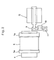
- FIG. 6 schematically shows a two-dimensional distribution measuring equipment of pH of the solution
- numeral 22 is a substrate, the top surface of which a cell 24 for accommodating the sample 23 such as the solution is formed.
- This substrate 22 imparts water resisting property to the sample 23 by providing resin mold.
- Numeral 25 is a reference electrode immersed in the sample 23, and by applying a specified voltage across the substrate 22 by the direct current power supply 26, this reference electrode 25 brings the potential of the sample 23 to a specified high level with respect to the substrate 22. The applied voltage causes the sensing section 6 to be in the depleted condition.
- the outputted signals are inputted as they are to the image output unit 27 such as televisions, etc. to output images, or the output signals may be AD-converted to be inputted to the computer.
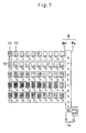
- FIG. 7 schematically shows the configuration of the top surface of the substrate 22, which comprises a plurality of sensor sections 13 for converting the pH to electric charges, an electric charge transfer section 8 for transferring electric charges converted at the sensor section 13 in the arrow direction, and an output section 14 for converting the transferred electric charges into output signals.
- the electric charge section 8 comprises horizontal CCD 8H and vertical CCD 8V.
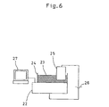
- FIG. 8 shows the construction of the sensor section 13.
- This sensor section 13 is formed as follows. That is, the p type Si substrate 2 which is made to be the substrate 22 is thermal oxidized to form the oxide film (SiO 2 ) 28, and part of the oxide film is etched and further thermal oxidized to form the gate oxide film 29.
- the film thickness of this gate oxide film 29 is about 500 ⁇ .
- electrodes 30, 31 are formed by depositing low-resistance P-doped poly-silicon to the portions corresponding to the electric charge injection controller section 5 and the barrier section 7 on the top surface, respectively.
- the film thickness of these electrodes 30, 31 is about 3000 ⁇ , and the film is thermal oxidized to about 1000 ⁇ after deposition. Thereafter, the P-doped low-resistance poly-silicon is deposited again and the electrode 32 is formed on the top surface of the electric charge transferring section 8. The film of this electrode 32 is thermal oxidized to about 1000 ⁇ after poly-silicon is deposited to the level similar to that of the electrodes 30, 31. Oxidizing the film in this way can hold insulation between electrodes. Thereafter, Si 3 N 4 . (Ta 2 O 3 or Al 2 O 3 acceptable) is deposited to about 700 ⁇ to form the sensing section 6. Numeral 33 designates an electrode formed with aluminum.
- FIG. 9 shows the other embodiment of the sensor section 13, and in the sensor section 13 shown in FIG. 9, a reference electrode is incorporated. That is, in this sensor section 13, in place of the electrode 30 of the electric charge injection controller section 5 shown in FIG. 8, a film 34 non-sensitive to pH is installed. The threshold value of the sensing section 6 is adjusted and the potential wells of the sensing section 6 are made deeper as compared to the electric charge injection controller section 5. In order to achieve electric connections between the sample and the substrate, an electrode 35 comprising inert metal such as platinum, etc. is installed.
- the electric charge injection controller section 5 and the sensing section 6 are designed to allow the sensing section 6 only to respond to pH and not to allow the electric charge injection controller section 5 to respond, but both are equally subject to influences such as external noises or potential variations at interface between the electrode 35 and the sample. That is, the difference of potential between the electric charge injection controller section 5 and the sensing section 6 reflects the pH value. Consequently, injecting electric charges to the sensing section 6 can convert the pH value to electric charges.
- the electric charge injection controller section 5 is portions that serve to allow the electric charges fed from the electric charge feeder section 4 to be leveled off by the sensing section 6, about 10 ⁇ m would be enough for their width.
- the barrier section 7 only works to prevent electric charges leveled off by the sensing section 6 from flowing into the electric charge transferring section 8 readily, and about 10 ⁇ m would be enough for the width.
- the sensing section 6 because a certain amount of electric charge amount to be leveled off is required in order to improve the measuring accuracy, the minimum required area is secured for the purpose, and it has a size about some 10 ⁇ m x some 10 ⁇ m to 100 ⁇ m x 100 ⁇ m.
- various sizes are set with the electric charge transferring section 8 and the floating diffusion 9 taken into account.
- the sizes of the sensing section 6, electric charge transferring section 8, and floating diffusion 9 were designed to be 100 ⁇ m x 100 ⁇ m, 50 ⁇ m x 200 ⁇ m. 21000 ⁇ m 2 . respectively, and measurement was carried out, and in the source follower circuit 17 using a 120 k ⁇ resistor 18 (see FIG. 5), about 80 mV output signals have been obtained per 1 pH.
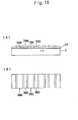
- FIG. 10 shows one example of the configuration of the electric charge transferring section 8, and FIG. 10 (A) shows a cross-sectional structure and FIG. 10 (B) a top surface structure, respectively.
- the electric charge transferring section 8 shown In FIG. 10 comprises CCD of 4-phase structure, and by depositing P-doped low-resistance poly-silicon in two layers in about 3000 ⁇ thickness on the top surface of the oxide film 29 to form four electrodes 36A, 36B. 36C, 36D. Each of the electrodes 36A to 36D are oxidized to about 1000 ⁇ in order to achieve insulation from one another.
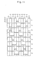
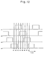
- FIG. 11 and FIG. 12 are illustrations for explaining the drive principle of the electric charge transferring section 8, and in particular, FIG. 11 shows the CCD drive voltage of the electric charge transferring section 8, and FIG. 12 is a timing chart of the CCD driving voltage. Symbols ⁇ 1 to ⁇ 4 in FIGs 11, 12 and 13 correspond to 36A to 36D, respectively.
- CCD drive in the electric charge transferring section 8 is not limited to the four phases, but one-phase drive, two-phase drive, etc. may be accepted, and suitably selected in accordance with the electric charge amount to be transferred. As the number of the sensor section 13 increases, the transfer efficiency causes big problems, but in such event, it is preferable to use a bulk channel with high transfer efficiency.
- the electric charge transferred by the electric charge transferring section 8 is transferred to the floating diffusion 9 (see FIG. 7) of the output section 14, and varies the potential of the floating diffusion 9. This potential variation is inputted to the gate of the output transistor 12, and the drain current of the output transistor 12 is read by the source follower circuit 17 (see FIG. 5).
- FIG. 13 shows characteristics of the source follower circuit 17, and this data is obtained when the MOS transistor of 200 ⁇ m in channel width and 50 ⁇ m in channel length is used for an output transistor 12 and the resistor 18 is set to various values.
- FIG. 13 indicates that by changing the value of the resistor 18 in the source follower circuit 17, the output value of the source follower circuit 17 is considerably changed.
- the area of the floating diffusion 9 should be made as small as possible, but excessively small area is easily saturated when Incoming electric charges are excessively many and measurement is unable to be carried out. Consequently, it is preferable to determine the area of the floating diffusion 9 and the resistance 18 in the source follower circuit 17 by the area of the sensing section 6 as well as drive voltage of the electric charge transferring section 8.
- FIG. 14 shows the output signal pulse of the source follower circuit 17 together with the output gate pulse and the reset gate pulse, and the output signal pulse is outputted in a complicated form as shown in FIG. 14, but the true signal is the portion shown with symbol IV in the figure. That is, the portion of symbol I is the pulse signal generated when the reset gate is turned on, and is the signal generated as long as the reset gate 10 is superimposed on the floating diffusion 9. The portion of symbol II is the signal under the electrically floating condition after the floating diffusion 9 is reset. The signal of symbol III is the pulse signal generated when the output gate is turned on.
- the signal expressed by symbol IV is the signal when the output gate closes and all the electric charges transferred flow into the floating diffusion 9, and the signal at this timing becomes the true signal.
- This signal IV is transformed into the output signal consisting of the true signal only by using the sample and hold circuit (not illustrated), and is outputted to the outside. This external output is inputted to the monitor 27 (see FIG. 6) and visualized.
- the manufacturing process of the two-dimensional pH distribution measuring equipment is described. This process is only one example, and the device fabricated by this process uses an electric charge transferring system of the surface channel.
- the transfer efficiency was about 98%, but as the number of pixels increases, the transfer loss becomes a problem. Therefore, when the number of pixels increases, it is preferable to use the bulk channel system in which electric charge transfer takes place inside the semiconductor 41.
- the pH at a plurality of positions of different solutions can be simultaneously measured. Since the pH simultaneously measured is converted to electric charges, the two-dimensional distribution of pH can be easily visualized by transferring the electric charges using the techniques such as CCD.
- two-dimensional distribution of pH was intended to be measured, but by chemical modifying the surface of the sensing section 6 with suitable sensitive material, the ion concentration other than pH can be measured. That is, this invention can be suitably and extensively used for two-dimensional distribution measurement of ion concentration of samples, such as solutions, as well as applied to the following fields.
- the measurement subjects may be gas, liquid, solid, or powders
- the embodiment can be applied to chemical sensing which selectively reacts by the specific sensitive layer of the sensor section as well as to any phenomena in which electric particles fluctuate at the interface by physical contact, and for example, the distribution of liquid flow or the distribution of transient phenomena of instantaneous chemical reactions can be obtained in the form of high-sensitivity high-quality chemical images.
- the embodiment is useful from real-time visualization of titration phenomena to other kinds of analysis and display by image software.
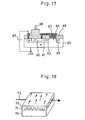
- FIG. 17 schematically shows one example of two-dimensional distribution measuring equipment of pressure
- numeral 60 designates a p-type Si substrate, 61 an N-well region of 1 ⁇ m or less formed at the surface of the substrate 60.
- Numeral 62 is a P ⁇ diffusion layer formed in the N-well region 61, and is an emitter section doped at the concentration higher than that in the substrate 60.
- a thick oxide film which is about 1 ⁇ m thick is provided, and stress is focused on the emitter of this PNP transistor.
- a contact hole is formed to install a metal electrode 63 to sweep up to the gate of the sensing section 64, and the potential of the P ⁇ diffusion layer 62 is applied to the sensing section 64.
- the oxide film only of this sensing section 64 is made to be 1000 ⁇ thick, and the oxide film around it is made to be 5000 ⁇ thick. This is to greatly vary the potential in the vicinity of the interface between the semiconductor and the oxide film for the sensing section 64 only by the potential of the metal electrode 63.
- Numeral 65 designates channel stoppers formed surrounding the circumference of the sensing section 64, and potentially separate the sensing section 64 from the circumference.
- Numeral 66 is an insulator, and 67 is a power supply that biases in the reverse direction across the substrate 60, the collector, and the N-well region 61, the base. Though not illustrated, an electric charge feeder section, barrier section, etc. are provided perpendicular to the paper surface.
- FIG. 18 is an illustration to schematically describing the measuring principle of the two-dimensional magnetic field distribution, and the insulating material 71 is accumulated on the top surface of the semiconductor substrate 70, and the semiconductor 72 is further accumulated on the top surface, and the current is allowed to flow in this semiconductor 72 in the arrow 73 direction.
- the substrate 70 is set in such a manner that the magnetic field direction 74 crosses at right angles to the direction of the current 73 and is parallel to the substrate 70, voltage is generated in the direction perpendicular to the surface of the substrate 70.
- the two-dimensional distribution of the magnetic field can be measured by converting the magnitude of this voltage to electric charges by the above-mentioned electric charge conversion mechanism.
- FIG. 19 schematically shows the construction of the sensor section of the magnetic field two-dimensional distribution measuring equipment configured on the basis of the measuring principle mentioned above, and FIG. 19 (A) shows a cross-sectional structure and FIG. 19 (B) a plane structure.
- numeral 74 designates a semiconductor substrate, 75 an electric charge feeder section, 76 an electric charge injection controller section, 77 a sensing section, 78 a barrier section, and 79 an electric charge transfer section.
- And numeral 80 is an epitaxial grown Si layer deposited only on the top surface of the sensing section 77, 81 electrodes comprising poly-silicon, and 82 an insulation layer comprising an epitaxial grown Al 2 O 3 insulation layer.
- the thickness of the Al 2 O 3 layer is set to about 1000 ⁇ at the bottom of the Si layer 80 and the poly-silicon electrodes 81, respectively, and is configured in such a manner that fluctuation of potential is positively generated.
- the magnetic field is in the direction shown with the arrow mark 83
- voltage by the magnetic field 83 is generated in the direction perpendicular to the semiconductor substrate 74, and the potential in the vicinity of the Interface between the semiconductor 70 and the insulation layer 82 comprising Al 2 O 3 fluctuates.
- the magnetic field two-dimensional distribution can be measured by converting this potential fluctuation into electric charges using the electric-charge conversion mechanism.
- the temperature two-dimensional distribution measuring equipment will be described.
- this measuring equipment the phenomenon in that the voltage across the emitter and the base of the PNP-transistor varies by the change of temperature is utilized, and this is nearly similar to the pressure two-dimensional distribution measuring equipment of the second embodiment (see FIG. 17) in this point. Consequently, in FIG. 20 that schematically shows the temperature two-dimensional distribution measuring equipment, like reference characters designate like or corresponding parts in FIG. 17.
- temperature at a small area is given to the emitter 62 by bringing the metal 90 with good thermal conductivity in contact with the emitter 62. Therefore, by supplying the generated voltage to the sensing section 64 and converting it to electrical charges using the electric charge conversion mechanism, the temperature two-dimensional distribution can be measured.
- the two-dimensional distributions of pH and temperature can be obtained simultaneously.
- the electrode 96 is installed throughout the full surface of the top surface of the device 95 and a sample 97 (any of solid, liquid, or gas) is located in the form of sandwich between this electrode 96 and the device 95, and voltage is applied across the device 95 and the electrode 96 under this condition.
- a sample 97 any of solid, liquid, or gas
- the sample with different resistivity 97 gives potentials varying at relevant positions to the device 95, and by converting this voltage to electric charges, it is possible to detect the two-dimensional distribution of the sample 97.
- numeral 98 designates the bias power supply.
- the measuring method of the physical phenomena or chemical phenomena of this invention phenomena in multiple different positions can be simultaneously detected. And since the physical or chemical quantity is converted to the electric charges, the two-dimensional distribution of the physical or the chemical phenomena can be easily visualized by the use of CCD. Depending on the data processing method, it is also possible to obtain the three-dimensional distribution.
Description
- The present invention relates to a measuring method and equipment for quantifying various physical phenomena or chemical phenomena.
- Conventionally, it is light that converts physical phenomena or chemical phenomena into electric charges for measurement. Irradiating photo-diodes with the light generates electron-hole pairs corresponding to the light quantity, and the light quantity is changed to quantity of electric charges, and the light quantity is measured by evaluating the quantity of electric charges.
- However, in physical and chemical phenomena other than light, in almost all cases, they are converted to electric signals such as voltage values, electric current values, resistance values, etc., and these values are read.
- For example, there are thermocouples using the Seebeck effect in which potential difference is generated on both ends when different temperatures are applied to both ends of a certain metal wire. This is intended to join two kinds of different metals and the temperature of the joined portion is determined from the potential difference generated at both ends. The measurement of pH using ISFET (ion-sensitive field-effect transistor) is achieved by changing the channel conductance below the pH-sensitive gate insulator by absorbing the hydrogen ion, and measuring the pH value of the solution by measuring the drain current.
- In either of the measurement methods illustrated above, accumulation and transfer, which are handling methods special to electric charges, are unable to be carried out, and it is extremely difficult to simultaneously take in information at a plurality of points and process at high speed or visualize the measurement results.
- Now, for physical phenomena or chemical phenomena, there are various phenomena such as concentration, temperature, magnetic field, pressure, acceleration, velocity, sound wave, ultrasonic wave, oxidation-reduction potential, reaction velocity, etc., and these phenomena can be converted into various electric signals (current, voltage, resistance, capacity, potential) by the use of conventional technologies, but it is the main object of this invention to handle these phenomena in a manner special to electric charges by converting these phenomena into electric charges and to carry out quantification special to electric charges.
- In IBM Technical Disclosure Bulletin,
volume 14, no. 11. page 3420, XP 002111424 New York, US, with the title "Charge Coupled Device Magnetic Field Sensor. April 1972", there is disclosed a charge-coupled-device for allowing an electric current to flow. The magnetic field is measured by catching the behaviour of electric charges when the electric current is allowed to flow. In the equipment disclosed in that document, one magnetic field sensor is located at a certain measuring place. The electric current is allowed to flow by use of CCD-electrodes. Similar structures are disclosed in US-A-5 194 750 as well as in EP-A-0 733 911. According to those documents, the turning condition of the current is caught and measured via the magnetic field. - Consequently, in each of the equipments disclosed in the above-mentioned documents, the CCD-structure is required at each one of the measuring places, thus resulting in an extremely big structure. However, when the construction becomes large, for example, in viewing the two-dimensional distribution of the magnetic field, an extremely large area is required, and therefore such a construction is not suitable for measuring the two-dimensional distribution of, for instance, the magnetic field of a microscopic region.
- Therefore, it is an object of this invention to provide a method and equipment that can easily visualize various physical phenomena or chemical phenomena by simultaneously taking in data at a plurality of points and carrying out accumulation and transfer.
- To solve this object the present invention provides a method and an equipment as specified in
claims - The method of measuring physical phenomena or chemical phenomena of this invention uses potential wells configured to change the depth corresponding to the magnitude of the physical or chemical quantity, to inject electric charges into these potential wells, and to convert the physical or chemical amount to electric charges corresponding to the depth of the potential wells.
- The equipment of measuring physical or chemical phenomena of this invention is configured to one-dimensionally or two-dimensionally array a plurality of potential wells configured to change the depth corresponding to the magnitude of the physical or chemical quantity, to inject electric charges into these potential wells, and to convert the physical or chemical amount to electric charges corresponding to the depth of the potential wells.
- By this configuration, it is possible to simultaneously measure phenomena at a plurality of different positions. Because the physical or chemical quantity is converted into electric charges, it is possible to easily visualize the one-dimensional distribution or two-dimensional distribution of physical or chemical phenomena by using CCD (charge coupled device).
- Further details, objects and advantages of the present invention will become apparent from the following description when taken in conjunction with the drawings, in which:
- Fig. 1 is an illustration showing the basic construction of the equipment for measuring physical phenomena or chemical phenomena of this invention;
- Fig. 2 is an illustration schematically showing the principal portion of the equipment;
- Fig. 3 is an illustration for explaining the measuring principle of the equipment;
- Fig. 4 is an illustration for explaining other measuring principle;
- Fig. 5 is an illustration showing one example of the source follower circuit connected to the above-mentioned equipment;
- Fig. 6 is a longitudinal cross-sectional view schematically showing the equipment according to the first embodiment;
- Fig. 7 is a plan view schematically showing the construction of the principal portion of the above-mentioned equipment;
- Fig. 8 is a longitudinal cross-sectional view showing one example of the sensor portion of the above-mentioned equipment;
- Fig. 9 is a longitudinal cross-sectional view showing the other example of the sensor portion of the above-mentioned equipment;
- Fig. 10 shows one example of the electric charge transfer section of the above-mentioned equipment, and (A) is a longitudinal cross-sectional view and (B) a plan view;
- Fig. 11 is a CCD drive potential diagram of the above-mentioned electric charge transfer section;
- Fig. 12 is a timing chart of CCD drive voltage of the above-mentioned electric charge transfer section;
- FIG. 13 is a diagram showing the characteristics of the source follower circuit;
- FIG. 14 is a diagram showing signals of each section of the above-mentioned source follower circuit;
- FIG. 15 is a diagram showing one example of the manufacturing process of the equipment according to the first embodiment together with FIG. 16;
- FIG. 16 is a diagram showing one example of the manufacturing process of the equipment according to the first embodiment together with FIG. 15;
- FIG. 17 is a longitudinal cross-sectional view schematically showing the equipment according to the second embodiment;
- FIG. 18 is an illustration for schematically illustrating the measuring principle of the two-dimensional magnetic field distribution;
- FIG. 19 is an illustration schematically showing the equipment according to the third embodiment, and (A) is a longitudinal cross-sectional view and (B) a plan view;
- FIG. 20 is a longitudinal cross-sectional view schematically showing the equipment according to the fourth embodiment;
- FIG. 21 is an illustration showing another embodiment; and
- FIG. 22 is an illustration showing still another embodiment.
- Referring now to the drawings, preferred embodiments according to the invention will be described in detail hereinafter. First of all, FIG. 1 shows a basic construction of the
equipment 1 for measuring physical phenomena or chemical phenomena according to this invention, and in this figure,numeral 2 denotes a semiconductor substrate comprising, for example, p type Si (silicon) which is about 500 µm thick. - To the
semiconductor substrate 2,channel stoppers 3, an electriccharge feeder section 4, electric chargeinjection controller section 5,sensing section 6 as electric charge converting section,barrier section 7, electriccharge transfer section 8,floating diffusion 9,reset gate 10,reset drain 11, and output transistor ofMOS structure 12 are formed. - A
sensor section 13 is formed by members of the electriccharge feeder section 4, electric chargeinjection controller section 5,sensing section 6, andbarrier section 7, and thesensing section 6 comprises potential wells configured to change the depth in accord with the magnitude of the physical or chemical quantity as later discussed. Anoutput section 14 is formed by members of thefloating diffusion 9,reset gate 10, resetdrain 11, andoutput transistor 12. - By arraying the
sensor section 13 two-dimensionally as shown in FIG. 7, data at a plurality of points are simultaneously taken in, and the signals at a plurality of points can be orderly processed by the electriccharge transfer section 8 and theoutput section 14. The processing procedure will be later described in detail referring to embodiments. Thesensor section 13 may be one-dimensionally arrayed. - FIG. 2 is an illustration schematically showing the plane configuration of the
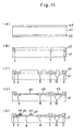
sensor section 13 and the portion connected to this, and in FIG. 2,numeral 5a denotes an electric charge injection controller section electrode, and 7a a barrier section electrode. Next description will be made on the measuring principle by the measuring equipment referring to the potential diagram shown in FIG. 3. In measurement, the pulse voltage is applied to the electriccharge feeder section 4,barrier section 7, and resetgate 10, while direct current voltage is applied to other electrodes excluding thefloating diffusion 9. - Now, in general, In the MOS structure using the p type semiconductor, it is known that applying the positive voltage to the metal electrode allows the depletion layer to form at the interface between the insulator and the semiconductor in accordance with the voltage. Therefore, using this phenomenon, as shown in FIG. 3, the potential condition is formed at the semiconductor-insulation film interface.
- Under the
condition 1, the potential of the electriccharge feeder section 4 is set to a high level (higher in the arrow direction), and noelectric charge 15 is injected to thesensing section 6. - Under the
condition 2, as shown in FIG. 3 (B),electric charges 15 are charged into thesensing section 6 by lowering the potential of the electriccharge feeder section 4. - Under the
condition 3, as shown In FIG. 3 (C),electric charges 15a leveled off by the electric chargeinjection controller section 5 are accumulated in thesensing section 6 by raising the potential of the electriccharge feeder section 4. - Under the
condition 4, as shown in FIG. 3 (D), theelectric charges 15a accumulated in thesensing section 6 are transferred to the floatingdiffusion 9 by raising the potential of thebarrier section 7. - Under the
condition 5, as shown in FIG. 3 (E), thebarrier section 7 is closed after all theelectric charges 15a of thesensing section 6 are transferred to the floatingdiffusion 9 and flow-in of electric charges is stopped. Under this stage, the potential of the floatingdiffusion 9 is determined by the amount of transferredelectric charges 15a, and this potential is inputted to the gate section of theoutput transistor 12 of the MOS structure, and the drain current of thisoutput transistor 12 is measured with thesource follower circuit 17 as shown in FIG. 5. - Under the
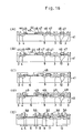
condition 6, as shown in FIG. 3 (F), thereset gate 10 is turned on and reset to the potential of thereset drain 11 after the potential of the floatingdiffusion 9 is read. By this resetting, the condition returns to that same as thecondition 1 again. That is, by repeating the operations ofcondition 1 tocondition 6, electric charges can be outputted to the outside. - FIG. 4 shows the other embodiment of the measuring equipment, and in this measuring equipment, the
first barrier section 7A, electriccharge accumulation section 16, and the second barrier section 7B are provided after thesensing portion 6, and theelectric charges 15b for several terms are accumulated at the electriccharge accumulation section 16, and after a certain amount of electric charges is accumulated, the potential of the second barrier section 7B is raised, and the electric charges accumulated at the electriccharge accumulation section 16 are transferred to the electriccharge transfer section 8. In the measuring equipment configured in this way, the sensitivity becomes several times, and it is possible to carry out measurement at higher accuracy. - As understood from the explanation concerning FIG. 3 and FIG. 4, in this measuring equipment, there used is an electric charge conversion mechanism for forming potential wells (sensing section 6) configured to vary the depth in accordance with the magnitude of the physical or chemical quantity on the
semiconductor substrate 2, injectingelectric charges 15 to thepotential wells 6, and converting the physical or chemical quantity to electric charges in accordance with the depth of these potential wells. - In the measuring equipment shown in FIG. 3 and FIG. 4, the potential of the electric
charge feeder section 4 is raised and lowered to level off the electric charges accumulated at thesensing section 6, but in place of this configuration, it is allowed to hold the potential of the electriccharge feeder section 4 constant, raise and lower the level of the electric chargeinjection controller section 5, and level off electric charges accumulated at thesensing section 6. - FIG. 5 shows one example of the
source follower circuit 17, which comprises aresistor 18,output terminal 19, and groundingterminal 20, and the output signal in thiscircuit 17 greatly varies in accordance with the size of theresistor 18 connected as shown in FIG. 13 but linear voltage signals can be obtained with respect to the output current.Numeral 21 designates a monitor equipped with data processing capabilities or image processing capabilities connected to theoutput terminal 19. - Referring now to FIG. 6 and after, various measuring equipment with the electric load conversion mechanism built in will be explained.
- For the first embodiment, description will be made on an equipment for measuring the two-dimensional distribution of the pH of the solution. FIG. 6 schematically shows a two-dimensional distribution measuring equipment of pH of the solution, and in FIG. 6, numeral 22 is a substrate, the top surface of which a
cell 24 for accommodating thesample 23 such as the solution is formed. Thissubstrate 22 imparts water resisting property to thesample 23 by providing resin mold.Numeral 25 is a reference electrode immersed in thesample 23, and by applying a specified voltage across thesubstrate 22 by the directcurrent power supply 26, thisreference electrode 25 brings the potential of thesample 23 to a specified high level with respect to thesubstrate 22. The applied voltage causes thesensing section 6 to be in the depleted condition. - In the pH two-dimensional distribution measuring equipment of the above-mentioned configuration, the outputted signals are inputted as they are to the
image output unit 27 such as televisions, etc. to output images, or the output signals may be AD-converted to be inputted to the computer. - FIG. 7 schematically shows the configuration of the top surface of the
substrate 22, which comprises a plurality ofsensor sections 13 for converting the pH to electric charges, an electriccharge transfer section 8 for transferring electric charges converted at thesensor section 13 in the arrow direction, and anoutput section 14 for converting the transferred electric charges into output signals. Theelectric charge section 8 compriseshorizontal CCD 8H and vertical CCD 8V. - FIG. 8 shows the construction of the
sensor section 13. Thissensor section 13 is formed as follows. That is, the ptype Si substrate 2 which is made to be thesubstrate 22 is thermal oxidized to form the oxide film (SiO2) 28, and part of the oxide film is etched and further thermal oxidized to form thegate oxide film 29. The film thickness of thisgate oxide film 29 is about 500 Å. andelectrodes injection controller section 5 and thebarrier section 7 on the top surface, respectively. - The film thickness of these
electrodes electrode 32 is formed on the top surface of the electriccharge transferring section 8. The film of thiselectrode 32 is thermal oxidized to about 1000 Å after poly-silicon is deposited to the level similar to that of theelectrodes sensing section 6.Numeral 33 designates an electrode formed with aluminum. - FIG. 9 shows the other embodiment of the
sensor section 13, and in thesensor section 13 shown in FIG. 9, a reference electrode is incorporated. That is, in thissensor section 13, in place of theelectrode 30 of the electric chargeinjection controller section 5 shown in FIG. 8, afilm 34 non-sensitive to pH is installed. The threshold value of thesensing section 6 is adjusted and the potential wells of thesensing section 6 are made deeper as compared to the electric chargeinjection controller section 5. In order to achieve electric connections between the sample and the substrate, anelectrode 35 comprising inert metal such as platinum, etc. is installed. The electric chargeinjection controller section 5 and thesensing section 6 are designed to allow thesensing section 6 only to respond to pH and not to allow the electric chargeinjection controller section 5 to respond, but both are equally subject to influences such as external noises or potential variations at interface between theelectrode 35 and the sample. That is, the difference of potential between the electric chargeinjection controller section 5 and thesensing section 6 reflects the pH value. Consequently, injecting electric charges to thesensing section 6 can convert the pH value to electric charges. - Now description will be made on the width of the
electrodes 30 to 33, 35 and thesensing section 6. First of all, because as for theelectrodes 30 to 33, 35 the electric chargeinjection controller section 5 is portions that serve to allow the electric charges fed from the electriccharge feeder section 4 to be leveled off by thesensing section 6, about 10 µm would be enough for their width. Thebarrier section 7 only works to prevent electric charges leveled off by thesensing section 6 from flowing into the electriccharge transferring section 8 readily, and about 10 µm would be enough for the width. - For the
sensing section 6, because a certain amount of electric charge amount to be leveled off is required in order to improve the measuring accuracy, the minimum required area is secured for the purpose, and it has a size about some 10 µm x some 10 µm to 100 µm x 100 µm. For the size of thissensing section 6. various sizes are set with the electriccharge transferring section 8 and the floatingdiffusion 9 taken into account. Experimentally, the sizes of thesensing section 6, electriccharge transferring section 8, and floatingdiffusion 9 were designed to be 100 µm x 100 µm, 50 µm x 200 µm. 21000 µm2. respectively, and measurement was carried out, and in thesource follower circuit 17 using a 120 kΩ resistor 18 (see FIG. 5), about 80 mV output signals have been obtained per 1 pH. - FIG. 10 shows one example of the configuration of the electric
charge transferring section 8, and FIG. 10 (A) shows a cross-sectional structure and FIG. 10 (B) a top surface structure, respectively. The electriccharge transferring section 8 shown In FIG. 10 comprises CCD of 4-phase structure, and by depositing P-doped low-resistance poly-silicon in two layers in about 3000 Å thickness on the top surface of theoxide film 29 to form fourelectrodes electrodes 36A to 36D are oxidized to about 1000 Å in order to achieve insulation from one another. - FIG. 11 and FIG. 12 are illustrations for explaining the drive principle of the electric
charge transferring section 8, and in particular, FIG. 11 shows the CCD drive voltage of the electriccharge transferring section 8, and FIG. 12 is a timing chart of the CCD driving voltage. Symbols ∅ 1 to ∅ 4 in FIGs 11, 12 and 13 correspond to 36A to 36D, respectively. - CCD drive in the electric
charge transferring section 8 is not limited to the four phases, but one-phase drive, two-phase drive, etc. may be accepted, and suitably selected in accordance with the electric charge amount to be transferred. As the number of thesensor section 13 increases, the transfer efficiency causes big problems, but in such event, it is preferable to use a bulk channel with high transfer efficiency. - The electric charge transferred by the electric
charge transferring section 8 is transferred to the floating diffusion 9 (see FIG. 7) of theoutput section 14, and varies the potential of the floatingdiffusion 9. This potential variation is inputted to the gate of theoutput transistor 12, and the drain current of theoutput transistor 12 is read by the source follower circuit 17 (see FIG. 5). - FIG. 13 shows characteristics of the
source follower circuit 17, and this data is obtained when the MOS transistor of 200 µm in channel width and 50 µm in channel length is used for anoutput transistor 12 and theresistor 18 is set to various values. FIG. 13 indicates that by changing the value of theresistor 18 in thesource follower circuit 17, the output value of thesource follower circuit 17 is considerably changed. - Now, In measuring the pH, to improve the measuring accuracy, a large change of output should be obtained with respect to the change in the amount of electric charges transferred to the floating
diffusion 9. To achieve this, the area of the floatingdiffusion 9 should be made as small as possible, but excessively small area is easily saturated when Incoming electric charges are excessively many and measurement is unable to be carried out. Consequently, it is preferable to determine the area of the floatingdiffusion 9 and theresistance 18 in thesource follower circuit 17 by the area of thesensing section 6 as well as drive voltage of the electriccharge transferring section 8. - FIG. 14 shows the output signal pulse of the
source follower circuit 17 together with the output gate pulse and the reset gate pulse, and the output signal pulse is outputted in a complicated form as shown in FIG. 14, but the true signal is the portion shown with symbol IV in the figure. That is, the portion of symbol I is the pulse signal generated when the reset gate is turned on, and is the signal generated as long as thereset gate 10 is superimposed on the floatingdiffusion 9. The portion of symbol II is the signal under the electrically floating condition after the floatingdiffusion 9 is reset. The signal of symbol III is the pulse signal generated when the output gate is turned on. - The signal expressed by symbol IV is the signal when the output gate closes and all the electric charges transferred flow into the floating
diffusion 9, and the signal at this timing becomes the true signal. This signal IV is transformed into the output signal consisting of the true signal only by using the sample and hold circuit (not illustrated), and is outputted to the outside. This external output is inputted to the monitor 27 (see FIG. 6) and visualized. - Referring now to FIG. 15 and FIG. 16, the manufacturing process of the two-dimensional pH distribution measuring equipment is described. This process is only one example, and the device fabricated by this process uses an electric charge transferring system of the surface channel.
- (1) First of all, a p-
type Si wafer 41 of about 10 Ωcm resistivity is wet-oxidized at 1100 °C for about 90 minutes using a thermal oxidation furnace, and oxide film (field oxide) 42 of about 6000 Å is formed on both top and bottom surfaces (see FIG. 15 (A)). - (2) Then,
channel stoppers 3 are formed (see FIG. 15 (B)). The method for forming thechannel stopper 3 is to etch thefield oxide 42 at the stopper forming places using hydrofluoric acid (HF), and to diffuse boron (B) at the places. The method for diffusing boron is, for example, to form by predeposition a solid diffusion source at 1100°C for 15 minutes together with thewafer 41, then, after removing the borosilicate glass, to drive-in oxidize at 1140°C for about 1 hour, and then, to anneal in the nitrogen gas atmosphere for about 10 minutes. - (3) The electric
charge feeder section 4, floatingdiffusion 9, and the source and the drain of theoutput transistor 12 are n-type diffusion regions (see FIG. 15 (C)), and these are formed in the same manner as in the case ofchannel stoppers 3 with the exception that the liquid phosphorous diffusion source is used for a diffusion source, and are formed in order of predeposition, drive-in oxidation, and annealing. - (4) The electric charge
injection controller section 5, sensingsection 6,barrier section 7, and electriccharge transferring section 8 must have the oxide film made thinner in order to allow the potential of the electrodes to exert great influences on the oxide film and the semiconductor interface. Consequently, as shown in FIG. 15 (D) thefield oxide 42 corresponding to these sections are etched with hydrofluoric acid, and then, it is oxidized at 1050 °C for about 2.5 hours, and annealed for about 20 minutes in the nitrogen gas atmosphere to form thegate oxide 43 in thickness of about 1000 Å. - (5) For the electrode, as already described, the P-doped low-resistance poly-silicon is used. First of all, using CVD, P-doped low-resistance poly-silicon is deposited to about 3000 Å. Using a photo-lithography, poly-silicon other than the electrode forming portions is etched with a reactive ion etching machine. Thereafter, poly-silicon is oxidized at 1140 °C for about 45 minutes to cover the poly-
silicon electrodes 44 at the electrode forming portions with theoxide film 45 at about 1000 Å (see FIG. 15 (E)). Theoxide film 45 is provided for insulating from the other poly-silicon electrode 46 formed by depositing an additional poly-silicon film in the next process (see FIG. 16 (A)). - (6) Then, poly-silicon is deposited In the similar process to the above, and
electrodes 46 are formed by carrying out patterning, and the poly-silicon electrode 46 are further covered with the oxide film 47 (see FIG. 16 (A)). Thisoxide film 47 is to successfully affix the nitride film (Si3N4) 48 In the subsequent process (see FIG. 16 (C)). - (7) Now, the
oxide film 43 at the portion where thesensing section 6 is formed is degraded after passing various processes after gate oxidation. Therefore, thisoxide film 43 is removed by the use of hydrofluoric acid and thegate oxide 43A of about 1000 Å is newly formed (see FIG. 16 (B)). - (8) In order to provide pH sensitivity and water resisting property, the
nitride film 48 is deposited to about 800 Å using CVD (see FIG. 16 (C)). - (9) Contact holes 49 are opened so that voltage can be applied from the outside to each of the electrodes and n-diffused layers, respectively (see FIG. 16 (D)).
- (10) In order to deposit aluminum to about 1 µm to form
electrodes 50 at the portions where contact holes 49 are formed, electrode patterns are formed by photo-lithography, and portions other than these portions are etched (see FIG. 16 (E)). - In the above fabrication method, since the surface channel is employed in which the electric charge transfer takes place at the
semiconductor 41 surface, the transfer efficiency was about 98%, but as the number of pixels increases, the transfer loss becomes a problem. Therefore, when the number of pixels increases, it is preferable to use the bulk channel system in which electric charge transfer takes place inside thesemiconductor 41. - According to the pH two-dimensional distribution measuring equipment of the above-configuration, the pH at a plurality of positions of different solutions can be simultaneously measured. Since the pH simultaneously measured is converted to electric charges, the two-dimensional distribution of pH can be easily visualized by transferring the electric charges using the techniques such as CCD.
- In the above-mentioned embodiment, two-dimensional distribution of pH was intended to be measured, but by chemical modifying the surface of the
sensing section 6 with suitable sensitive material, the ion concentration other than pH can be measured. That is, this invention can be suitably and extensively used for two-dimensional distribution measurement of ion concentration of samples, such as solutions, as well as applied to the following fields. - ① Applicable fields as chemical microscope
- Chemical: ion concentration measurement
- Electro-chemical field, gas distribution measurement field
- Two-dimensional observation and analysis of titration
- ② Environment measurement
- • Environment: application to bioremediation
- ③ Food inspection
- • Foods, microorganisms
- ④ ME field
- • Medical and ecological tissues: surface ion concentration measurement, cell surface potential measurement
- ⑤ Animal and plant field
- • Plants: surface potential distribution measurement of callus
- • Living being/front view animals
- ⑥ Corrosion measuring field
- • Metal: painting and coating of metal corrosion
- ⑦ Surface analysis such as zeta potential, etc.
- • Zeta potential of powders and ceramics
- The measurement subjects (samples) may be gas, liquid, solid, or powders, and the embodiment can be applied to chemical sensing which selectively reacts by the specific sensitive layer of the sensor section as well as to any phenomena in which electric particles fluctuate at the interface by physical contact, and for example, the distribution of liquid flow or the distribution of transient phenomena of instantaneous chemical reactions can be obtained in the form of high-sensitivity high-quality chemical images. In addition, the embodiment is useful from real-time visualization of titration phenomena to other kinds of analysis and display by image software.
- For the second embodiment, two-dimensional distribution measurement of pressure using a pressure sensor is described. FIG. 17 schematically shows one example of two-dimensional distribution measuring equipment of pressure, and in FIG. 17, numeral 60 designates a p-type Si substrate, 61 an N-well region of 1 µm or less formed at the surface of the
substrate 60.Numeral 62 is a P± diffusion layer formed in the N-well region 61, and is an emitter section doped at the concentration higher than that in thesubstrate 60. On this P±diffusion layer 62. a thick oxide film which is about 1 µm thick is provided, and stress is focused on the emitter of this PNP transistor. - On the P±
diffusion layer 62, a contact hole is formed to install ametal electrode 63 to sweep up to the gate of thesensing section 64, and the potential of the P±diffusion layer 62 is applied to thesensing section 64. The oxide film only of thissensing section 64 is made to be 1000 Å thick, and the oxide film around it is made to be 5000 Å thick. This is to greatly vary the potential in the vicinity of the interface between the semiconductor and the oxide film for thesensing section 64 only by the potential of themetal electrode 63.Numeral 65 designates channel stoppers formed surrounding the circumference of thesensing section 64, and potentially separate thesensing section 64 from the circumference.Numeral 66 is an insulator, and 67 is a power supply that biases in the reverse direction across thesubstrate 60, the collector, and the N-well region 61, the base. Though not illustrated, an electric charge feeder section, barrier section, etc. are provided perpendicular to the paper surface. - In the two-dimensional distribution measuring equipment of pressure, when
mechanical stress 68 is exerted to the PNP transistor in the direction perpendicular to the PNP junction surface, voltage across the emitter and the base varies and the potential of theemitter section 62 varies. This potential change is swept to thesensing section 64 using the metal electrode. By this change of the swept potential, the potential at the interface between the oxide film and the semiconductor of thesensing section 64 varies, and by injecting electric charges to it, the change in the potential is converted to the electric charge amount. - For the third embodiment, a magnetic field two-dimensional distribution measuring equipment is explained. For this magnetic field measurement, the Hall effect is utilized. First of all, FIG. 18 is an illustration to schematically describing the measuring principle of the two-dimensional magnetic field distribution, and the insulating
material 71 is accumulated on the top surface of thesemiconductor substrate 70, and thesemiconductor 72 is further accumulated on the top surface, and the current is allowed to flow in thissemiconductor 72 in thearrow 73 direction. When thesubstrate 70 is set in such a manner that themagnetic field direction 74 crosses at right angles to the direction of the current 73 and is parallel to thesubstrate 70, voltage is generated in the direction perpendicular to the surface of thesubstrate 70. The two-dimensional distribution of the magnetic field can be measured by converting the magnitude of this voltage to electric charges by the above-mentioned electric charge conversion mechanism. - FIG. 19 schematically shows the construction of the sensor section of the magnetic field two-dimensional distribution measuring equipment configured on the basis of the measuring principle mentioned above, and FIG. 19 (A) shows a cross-sectional structure and FIG. 19 (B) a plane structure. In FIG. 19, numeral 74 designates a semiconductor substrate, 75 an electric charge feeder section, 76 an electric charge injection controller section, 77 a sensing section, 78 a barrier section, and 79 an electric charge transfer section.
- And numeral 80 is an epitaxial grown Si layer deposited only on the top surface of the
sensing section Si layer 80 and the poly-silicon electrodes 81, respectively, and is configured in such a manner that fluctuation of potential is positively generated. - Now, if the magnetic field is in the direction shown with the
arrow mark 83, when the current is allowed to flow in theSi layer 80 as shown with the arrow mark 84, voltage by themagnetic field 83 is generated in the direction perpendicular to thesemiconductor substrate 74, and the potential in the vicinity of the Interface between thesemiconductor 70 and theinsulation layer 82 comprising Al2O3 fluctuates. The magnetic field two-dimensional distribution can be measured by converting this potential fluctuation into electric charges using the electric-charge conversion mechanism. - For the fourth embodiment, the temperature two-dimensional distribution measuring equipment will be described. In this measuring equipment, the phenomenon in that the voltage across the emitter and the base of the PNP-transistor varies by the change of temperature is utilized, and this is nearly similar to the pressure two-dimensional distribution measuring equipment of the second embodiment (see FIG. 17) in this point. Consequently, in FIG. 20 that schematically shows the temperature two-dimensional distribution measuring equipment, like reference characters designate like or corresponding parts in FIG. 17. However, what is different is that temperature at a small area is given to the
emitter 62 by bringing themetal 90 with good thermal conductivity in contact with theemitter 62. Therefore, by supplying the generated voltage to thesensing section 64 and converting it to electrical charges using the electric charge conversion mechanism, the temperature two-dimensional distribution can be measured. - Other physical phenomena or chemical phenomena, in almost all cases, can be converted to electrical signals such as voltage, current, etc., and converting these electrical signals to electric charges using the electric charge conversion mechanism, handling special to the electric charges can be achieved.
- Each of the above-mentioned embodiments is Intended to measure the two-dimensional distribution with respect to some specific physical phenomena or chemical phenomena by arraying the same sensor, but this invention shall not be limited to these, but by arraying a plurality of sensors of different kinds, a plurality of physical phenomena or chemical phenomena can be simultaneously measured.
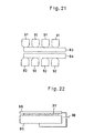
- For example, as shown in FIG. 21, by bringing and arranging a plurality of the
sensor section 91 for measuring the pH and thesensor section 92 for measuring temperature closer to one another and transferring electric charges obtained byrelevant sensor sections charge transfer sections - As shown in FIG. 22, the
electrode 96 is installed throughout the full surface of the top surface of thedevice 95 and a sample 97 (any of solid, liquid, or gas) is located in the form of sandwich between thiselectrode 96 and thedevice 95, and voltage is applied across thedevice 95 and theelectrode 96 under this condition. By this contrivance, the sample withdifferent resistivity 97 gives potentials varying at relevant positions to thedevice 95, and by converting this voltage to electric charges, it is possible to detect the two-dimensional distribution of thesample 97. By the way, numeral 98 designates the bias power supply. - According to the measuring method of the physical phenomena or chemical phenomena of this invention, phenomena in multiple different positions can be simultaneously detected. And since the physical or chemical quantity is converted to the electric charges, the two-dimensional distribution of the physical or the chemical phenomena can be easily visualized by the use of CCD. Depending on the data processing method, it is also possible to obtain the three-dimensional distribution.
- Because amplification of weak signals is possible by accumulating electric charges representing information of a plurality of points, it is possible to positively grasp microscopic changes of the phenomena.
Claims (4)
- A method of measuring a physical or chemical quantity, comprising the steps of:(a) providing in a sensor section (13) an array of potential wells configured to change their depth in accordance to the magnitude of the physical or chemical quantity to be measured.(b) injecting electric charges into said potential wells in order to convert the physical or chemical quantity to electric charges in accordance to the depth of the potential wells, and(c) transferring electric charges from said sensor section (13) to an output section (14).
- The method according to claim 1, wherein a potential of a sensing section (6) is changed for forming a potential condition in the vicinity of a semiconductor-insulation film interface.
- An equipment for measuring a physical or chemical quantity, comprising:(a) a semiconductor substrate (2);(b) a sensor section (13) formed on said semiconductor substrate and having an array of potential wells configured to change their depth in accordance to the magnitude of the physical or chemical quantity to be measured, the plurality of potential wells being arranged in a one-dimensional or two-dimensional array, wherein electric charges are injected in these potential wells and the physical or chemical quantity is converted into electric charges according to the depth of the potential wells;(c) a charge-coupled-device (CCD) formed on said semiconductor substrate (2) for transferring electric charges from the sensor section (13) to an output section (14).
- The equipment according to claim 3, wherein a potential of a sensing section (6) is changed for forming a potential condition in the vicinity of a semiconductor-insulation film interface.
Applications Claiming Priority (3)
| Application Number | Priority Date | Filing Date | Title |
|---|---|---|---|
| JP157716/97 | 1997-05-29 | ||
| JP15771697A JP4231560B2 (en) | 1997-05-29 | 1997-05-29 | Method and apparatus for electrochemical measurement of chemical quantity distribution |
| JP15771697 | 1997-05-29 |
Publications (3)
| Publication Number | Publication Date |
|---|---|
| EP0881486A2 EP0881486A2 (en) | 1998-12-02 |
| EP0881486A3 EP0881486A3 (en) | 1999-10-06 |
| EP0881486B1 true EP0881486B1 (en) | 2007-02-14 |
Family
ID=15655821
Family Applications (1)
| Application Number | Title | Priority Date | Filing Date |
|---|---|---|---|
| EP98109769A Expired - Lifetime EP0881486B1 (en) | 1997-05-29 | 1998-05-28 | Method for measuring physical phenomena or chemical phenomena and equipment thereof |
Country Status (4)
| Country | Link |
|---|---|
| US (1) | US6255678B1 (en) |
| EP (1) | EP0881486B1 (en) |
| JP (1) | JP4231560B2 (en) |
| DE (1) | DE69837060T2 (en) |
Families Citing this family (61)
| Publication number | Priority date | Publication date | Assignee | Title |
|---|---|---|---|---|
| US6627154B1 (en) * | 1998-04-09 | 2003-09-30 | Cyrano Sciences Inc. | Electronic techniques for analyte detection |
| JP2001244454A (en) * | 2000-02-29 | 2001-09-07 | Horiba Ltd | Molecule recognition type electrochemical ccd device |
| US7012306B2 (en) | 2001-03-07 | 2006-03-14 | Acreo Ab | Electrochemical device |
| JP2003014691A (en) * | 2001-06-29 | 2003-01-15 | Horiba Ltd | Ccd sensor |
| CN100429509C (en) * | 2001-11-16 | 2008-10-29 | 株式会社Bio-X | FET type sensor, ion density detecting method comprising this sensor, and base sequence detecting method |
| TW544752B (en) * | 2002-05-20 | 2003-08-01 | Univ Nat Yunlin Sci & Tech | Method for producing SnO2 gate ion sensitive field effect transistor (ISFET), and method and device for measuring the temperature parameters, drift and hysteresis values thereof |
| US8536661B1 (en) | 2004-06-25 | 2013-09-17 | University Of Hawaii | Biosensor chip sensor protection methods |
| WO2007008246A2 (en) | 2004-11-12 | 2007-01-18 | The Board Of Trustees Of The Leland Stanford Junior University | Charge perturbation detection system for dna and other molecules |
| JP4700335B2 (en) * | 2004-12-10 | 2011-06-15 | 株式会社堀場製作所 | Method and apparatus for measuring physical or chemical phenomena |
| JP4678676B2 (en) * | 2004-12-10 | 2011-04-27 | 株式会社堀場製作所 | Method or apparatus for measuring physical or chemical phenomena |
| KR101269508B1 (en) * | 2005-03-11 | 2013-05-30 | 고꾸리쯔 다이가꾸 호우징 도요하시 기쥬쯔 가가꾸 다이가꾸 | Cumulative chemical/physical phenomenon detecting apparatus |
| JP4641444B2 (en) * | 2005-03-31 | 2011-03-02 | 株式会社堀場製作所 | Potential measurement device for physical or chemical phenomena |
| JP5335415B2 (en) * | 2006-03-20 | 2013-11-06 | 国立大学法人豊橋技術科学大学 | Cumulative chemical / physical phenomenon detection method and apparatus |
| JP4852752B2 (en) * | 2006-04-04 | 2012-01-11 | 国立大学法人豊橋技術科学大学 | Chemical / physical phenomenon detector |
| US8349167B2 (en) | 2006-12-14 | 2013-01-08 | Life Technologies Corporation | Methods and apparatus for detecting molecular interactions using FET arrays |
| US11339430B2 (en) | 2007-07-10 | 2022-05-24 | Life Technologies Corporation | Methods and apparatus for measuring analytes using large scale FET arrays |
| EP2639579B1 (en) | 2006-12-14 | 2016-11-16 | Life Technologies Corporation | Apparatus for measuring analytes using large scale FET arrays |
| US8262900B2 (en) | 2006-12-14 | 2012-09-11 | Life Technologies Corporation | Methods and apparatus for measuring analytes using large scale FET arrays |
| CN102203282B (en) | 2008-06-25 | 2014-04-30 | 生命技术公司 | Methods and apparatus for measuring analytes using large scale FET arrays |
| US20100301398A1 (en) | 2009-05-29 | 2010-12-02 | Ion Torrent Systems Incorporated | Methods and apparatus for measuring analytes |
| US20100137143A1 (en) | 2008-10-22 | 2010-06-03 | Ion Torrent Systems Incorporated | Methods and apparatus for measuring analytes |
| JP2010122090A (en) * | 2008-11-20 | 2010-06-03 | Rohm Co Ltd | Ion image sensor and damage measuring device |
| CN101592627B (en) * | 2009-03-19 | 2012-12-05 | 中国科学院苏州纳米技术与纳米仿生研究所 | Method for manufacturing and integrating multichannel high-sensitive biosensor |
| US8673627B2 (en) | 2009-05-29 | 2014-03-18 | Life Technologies Corporation | Apparatus and methods for performing electrochemical reactions |
| US20120261274A1 (en) | 2009-05-29 | 2012-10-18 | Life Technologies Corporation | Methods and apparatus for measuring analytes |
| US8574835B2 (en) | 2009-05-29 | 2013-11-05 | Life Technologies Corporation | Scaffolded nucleic acid polymer particles and methods of making and using |
| US8776573B2 (en) | 2009-05-29 | 2014-07-15 | Life Technologies Corporation | Methods and apparatus for measuring analytes |
| TWI580955B (en) | 2010-06-30 | 2017-05-01 | 生命技術公司 | Ion-sensing charge-accumulation circuits and methods |
| US8487790B2 (en) | 2010-06-30 | 2013-07-16 | Life Technologies Corporation | Chemical detection circuit including a serializer circuit |
| US20120001646A1 (en) | 2010-06-30 | 2012-01-05 | Life Technologies Corporation | Methods and apparatus for testing isfet arrays |
| US11307166B2 (en) | 2010-07-01 | 2022-04-19 | Life Technologies Corporation | Column ADC |
| JP5876044B2 (en) | 2010-07-03 | 2016-03-02 | ライフ テクノロジーズ コーポレーション | Chemically sensitive sensor with lightly doped drain |
| US9618475B2 (en) | 2010-09-15 | 2017-04-11 | Life Technologies Corporation | Methods and apparatus for measuring analytes |
| WO2012039812A1 (en) | 2010-09-24 | 2012-03-29 | Life Technologies Corporation | Matched pair transistor circuits |
| JP5773357B2 (en) * | 2011-07-01 | 2015-09-02 | 国立大学法人豊橋技術科学大学 | Chemical / physical phenomenon detection apparatus and detection method |
| JP2013050426A (en) * | 2011-08-31 | 2013-03-14 | Chiba Univ | Method of detecting influenza virus rna using fet-type sensor |
| US9970984B2 (en) | 2011-12-01 | 2018-05-15 | Life Technologies Corporation | Method and apparatus for identifying defects in a chemical sensor array |
| US8821798B2 (en) | 2012-01-19 | 2014-09-02 | Life Technologies Corporation | Titanium nitride as sensing layer for microwell structure |
| US8747748B2 (en) | 2012-01-19 | 2014-06-10 | Life Technologies Corporation | Chemical sensor with conductive cup-shaped sensor surface |
| US8786331B2 (en) | 2012-05-29 | 2014-07-22 | Life Technologies Corporation | System for reducing noise in a chemical sensor array |
| WO2014025044A1 (en) * | 2012-08-10 | 2014-02-13 | 国立大学法人豊橋技術科学大学 | Device for measuring oxidation-reduction potential and method for measuring oxidation-reduction potential |
| US9080968B2 (en) | 2013-01-04 | 2015-07-14 | Life Technologies Corporation | Methods and systems for point of use removal of sacrificial material |
| US9841398B2 (en) | 2013-01-08 | 2017-12-12 | Life Technologies Corporation | Methods for manufacturing well structures for low-noise chemical sensors |
| US8962366B2 (en) | 2013-01-28 | 2015-02-24 | Life Technologies Corporation | Self-aligned well structures for low-noise chemical sensors |
| US8841217B1 (en) | 2013-03-13 | 2014-09-23 | Life Technologies Corporation | Chemical sensor with protruded sensor surface |
| US8963216B2 (en) | 2013-03-13 | 2015-02-24 | Life Technologies Corporation | Chemical sensor with sidewall spacer sensor surface |
| JP2016510895A (en) | 2013-03-15 | 2016-04-11 | ライフ テクノロジーズ コーポレーション | Chemical sensor with consistent sensor surface area |
| EP2972281B1 (en) | 2013-03-15 | 2023-07-26 | Life Technologies Corporation | Chemical device with thin conductive element |
| US9835585B2 (en) | 2013-03-15 | 2017-12-05 | Life Technologies Corporation | Chemical sensor with protruded sensor surface |
| US20140336063A1 (en) | 2013-05-09 | 2014-11-13 | Life Technologies Corporation | Windowed Sequencing |
| US10458942B2 (en) | 2013-06-10 | 2019-10-29 | Life Technologies Corporation | Chemical sensor array having multiple sensors per well |
| JP6493955B2 (en) * | 2014-10-09 | 2019-04-03 | ラピスセミコンダクタ株式会社 | Semiconductor device and manufacturing method of semiconductor device |
| JP6228098B2 (en) | 2014-10-20 | 2017-11-08 | シャープ株式会社 | Chemical / physical phenomenon detection device and manufacturing method thereof |
| CN107250784B (en) | 2014-12-18 | 2020-10-23 | 生命科技公司 | High data rate integrated circuit with transmitter configuration |
| CN111505087A (en) | 2014-12-18 | 2020-08-07 | 生命科技公司 | Method and apparatus for measuring analytes using large scale FET arrays |
| US10077472B2 (en) | 2014-12-18 | 2018-09-18 | Life Technologies Corporation | High data rate integrated circuit with power management |
| US9976981B2 (en) * | 2015-01-14 | 2018-05-22 | National University Corporation Toyohashi University Of Technology | Device for detecting chemical/physical phenomenon having a diffusion layer formed between an input charge control region and a sensing region on a substrate |
| DE102015214387B4 (en) * | 2015-07-29 | 2017-07-27 | Robert Bosch Gmbh | Sensor element for detecting at least one property of a sample gas in a sample gas space and method for producing the same |
| JP6307058B2 (en) * | 2015-12-03 | 2018-04-04 | シャープ株式会社 | Ion concentration sensor and ion concentration measuring method |
| JP6447925B2 (en) | 2015-12-15 | 2019-01-09 | シャープ株式会社 | Ion concentration sensor |
| JP2017167064A (en) * | 2016-03-17 | 2017-09-21 | 株式会社東芝 | Electrochemical sensor and measurement method using the same |
Family Cites Families (5)
| Publication number | Priority date | Publication date | Assignee | Title |
|---|---|---|---|---|
| EP0509141A1 (en) * | 1991-04-11 | 1992-10-21 | Landis & Gyr Business Support AG | Magnetic field sensor |
| US5374834A (en) * | 1993-10-12 | 1994-12-20 | Massachusetts Institute Of Technology | Ionic liquid-channel charge-coupled device |
| US5591996A (en) * | 1995-03-24 | 1997-01-07 | Analog Devices, Inc. | Recirculating charge transfer magnetic field sensor |
| JP2877047B2 (en) * | 1995-10-25 | 1999-03-31 | 日本電気株式会社 | Solid-state imaging device |
| US5789745A (en) * | 1997-10-28 | 1998-08-04 | Sandia Corporation | Ion mobility spectrometer using frequency-domain separation |
-
1997
- 1997-05-29 JP JP15771697A patent/JP4231560B2/en not_active Expired - Lifetime
-
1998
- 1998-05-27 US US09/085,693 patent/US6255678B1/en not_active Expired - Lifetime
- 1998-05-28 DE DE69837060T patent/DE69837060T2/en not_active Expired - Fee Related
- 1998-05-28 EP EP98109769A patent/EP0881486B1/en not_active Expired - Lifetime
Also Published As
| Publication number | Publication date |
|---|---|
| DE69837060D1 (en) | 2007-03-29 |
| US6255678B1 (en) | 2001-07-03 |
| EP0881486A3 (en) | 1999-10-06 |
| JP4231560B2 (en) | 2009-03-04 |
| EP0881486A2 (en) | 1998-12-02 |
| DE69837060T2 (en) | 2007-11-22 |
| JPH10332423A (en) | 1998-12-18 |
Similar Documents
| Publication | Publication Date | Title |
|---|---|---|
| EP0881486B1 (en) | Method for measuring physical phenomena or chemical phenomena and equipment thereof | |
| US7049645B2 (en) | FET type sensor, ion density detecting method comprising this sensor, and base sequence detecting method | |
| TWI547688B (en) | Ion-sensing charge-accumulation circuits and methods | |
| EP1870703B1 (en) | Cumulative chemical or physical phenomenon detecting apparatus | |
| JP4678676B2 (en) | Method or apparatus for measuring physical or chemical phenomena | |
| Barbaro et al. | A charge-modulated FET for detection of biomolecular processes: conception, modeling, and simulation | |
| US6294133B1 (en) | Multiple detecting apparatus for physical phenomenon and/or chemical phenomenon | |
| EP2653861A2 (en) | Methods and apparatus for measuring analytes using large scale FET arrays | |
| JP2006284225A (en) | Potential measuring method and measuring instrument | |
| JP5706684B2 (en) | Biosensor for electrochemical and / or electrical measurement, diamond electrode, and electronic integrated circuit | |
| JP3623728B2 (en) | Cumulative chemical / physical phenomenon detector | |
| TW465055B (en) | Method and apparatus for measurement of temperature parameter of ISFET using amorphous silicon hydride as sensor membrane | |
| JP4641444B2 (en) | Potential measurement device for physical or chemical phenomena | |
| CN101122571B (en) | Light excitation field addressing semiconductor transducer | |
| TWI777376B (en) | Biological detecting chip and biological detecting method | |
| WO2009064166A2 (en) | An integrated ion sensitive field effect transistor sensor | |
| JP4308374B2 (en) | Chemical quantity two-dimensional distribution measuring device | |
| US7015963B2 (en) | CCD sensor incorporating parallel diffusion regions within the output | |
| JP2002009274A (en) | Chemical ccd sensor | |
| JP3663018B2 (en) | Transient phenomena observation device at the interface between different materials | |
| WO2005036156A1 (en) | Detection of molecular interactions using a metal-insulator-semiconductor diode structure | |
| JP2005337806A (en) | Measuring method or physical or chemical phenomenon or its measuring instrument | |
| JP4700335B2 (en) | Method and apparatus for measuring physical or chemical phenomena | |
| JP2000065786A (en) | APPARATUS FOR MEASURING pH DISTRIBUTION OF ELECTROLYTE | |
| JP2001050897A (en) | Chemical two-dimensional distribution-measuring device |
Legal Events
| Date | Code | Title | Description |
|---|---|---|---|
| PUAI | Public reference made under article 153(3) epc to a published international application that has entered the european phase |
Free format text: ORIGINAL CODE: 0009012 |
|
| AK | Designated contracting states |
Kind code of ref document: A2 Designated state(s): DE FR GB IT |
|
| AX | Request for extension of the european patent |
Free format text: AL;LT;LV;MK;RO;SI |
|
| PUAL | Search report despatched |
Free format text: ORIGINAL CODE: 0009013 |
|
| RIC1 | Information provided on ipc code assigned before grant |
Free format text: 6G 01N 27/414 A, 6G 01N 27/00 B |
|
| AK | Designated contracting states |
Kind code of ref document: A3 Designated state(s): AT BE CH CY DE DK ES FI FR GB GR IE IT LI LU MC NL PT SE |
|
| AX | Request for extension of the european patent |
Free format text: AL;LT;LV;MK;RO;SI |
|
| 17P | Request for examination filed |
Effective date: 19991020 |
|
| AKX | Designation fees paid |
Free format text: DE FR GB IT |
|
| 17Q | First examination report despatched |
Effective date: 20041001 |
|
| GRAP | Despatch of communication of intention to grant a patent |
Free format text: ORIGINAL CODE: EPIDOSNIGR1 |
|
| GRAS | Grant fee paid |
Free format text: ORIGINAL CODE: EPIDOSNIGR3 |
|
| GRAA | (expected) grant |
Free format text: ORIGINAL CODE: 0009210 |
|
| AK | Designated contracting states |
Kind code of ref document: B1 Designated state(s): DE FR GB IT |
|
| REG | Reference to a national code |
Ref country code: GB Ref legal event code: FG4D |
|
| REF | Corresponds to: |
Ref document number: 69837060 Country of ref document: DE Date of ref document: 20070329 Kind code of ref document: P |
|
| ET | Fr: translation filed | ||
| PLBE | No opposition filed within time limit |
Free format text: ORIGINAL CODE: 0009261 |
|
| STAA | Information on the status of an ep patent application or granted ep patent |
Free format text: STATUS: NO OPPOSITION FILED WITHIN TIME LIMIT |
|
| 26N | No opposition filed |
Effective date: 20071115 |
|
| PGFP | Annual fee paid to national office [announced via postgrant information from national office to epo] |
Ref country code: DE Payment date: 20080605 Year of fee payment: 11 |
|
| PGFP | Annual fee paid to national office [announced via postgrant information from national office to epo] |
Ref country code: IT Payment date: 20080526 Year of fee payment: 11 |
|
| PGFP | Annual fee paid to national office [announced via postgrant information from national office to epo] |
Ref country code: GB Payment date: 20080528 Year of fee payment: 11 |
|
| GBPC | Gb: european patent ceased through non-payment of renewal fee |
Effective date: 20090528 |
|
| REG | Reference to a national code |
Ref country code: FR Ref legal event code: ST Effective date: 20100129 |
|
| PG25 | Lapsed in a contracting state [announced via postgrant information from national office to epo] |
Ref country code: FR Free format text: LAPSE BECAUSE OF NON-PAYMENT OF DUE FEES Effective date: 20090602 |
|
| PGFP | Annual fee paid to national office [announced via postgrant information from national office to epo] |
Ref country code: FR Payment date: 20080514 Year of fee payment: 11 |
|
| PG25 | Lapsed in a contracting state [announced via postgrant information from national office to epo] |
Ref country code: GB Free format text: LAPSE BECAUSE OF NON-PAYMENT OF DUE FEES Effective date: 20090528 |
|
| PG25 | Lapsed in a contracting state [announced via postgrant information from national office to epo] |
Ref country code: DE Free format text: LAPSE BECAUSE OF NON-PAYMENT OF DUE FEES Effective date: 20091201 |
|
| PG25 | Lapsed in a contracting state [announced via postgrant information from national office to epo] |
Ref country code: IT Free format text: LAPSE BECAUSE OF NON-PAYMENT OF DUE FEES Effective date: 20090528 |