EP0875927B1 - Method of manufacturing FET devices with maskless shallow trench isolation (STI) - Google Patents
Method of manufacturing FET devices with maskless shallow trench isolation (STI) Download PDFInfo
- Publication number
- EP0875927B1 EP0875927B1 EP98303125A EP98303125A EP0875927B1 EP 0875927 B1 EP0875927 B1 EP 0875927B1 EP 98303125 A EP98303125 A EP 98303125A EP 98303125 A EP98303125 A EP 98303125A EP 0875927 B1 EP0875927 B1 EP 0875927B1
- Authority
- EP
- European Patent Office
- Prior art keywords
- layer
- mesas
- silicon
- dummy
- pad
- Prior art date
- Legal status (The legal status is an assumption and is not a legal conclusion. Google has not performed a legal analysis and makes no representation as to the accuracy of the status listed.)
- Expired - Lifetime
Links
Images





Classifications
-
- H—ELECTRICITY
- H10—SEMICONDUCTOR DEVICES; ELECTRIC SOLID-STATE DEVICES NOT OTHERWISE PROVIDED FOR
- H10W—GENERIC PACKAGES, INTERCONNECTIONS, CONNECTORS OR OTHER CONSTRUCTIONAL DETAILS OF DEVICES COVERED BY CLASS H10
- H10W10/00—Isolation regions in semiconductor bodies between components of integrated devices
- H10W10/01—Manufacture or treatment
- H10W10/011—Manufacture or treatment of isolation regions comprising dielectric materials
- H10W10/014—Manufacture or treatment of isolation regions comprising dielectric materials using trench refilling with dielectric materials, e.g. shallow trench isolations
- H10W10/0143—Manufacture or treatment of isolation regions comprising dielectric materials using trench refilling with dielectric materials, e.g. shallow trench isolations comprising concurrently refilling multiple trenches having different shapes or dimensions
-
- H—ELECTRICITY
- H10—SEMICONDUCTOR DEVICES; ELECTRIC SOLID-STATE DEVICES NOT OTHERWISE PROVIDED FOR
- H10W—GENERIC PACKAGES, INTERCONNECTIONS, CONNECTORS OR OTHER CONSTRUCTIONAL DETAILS OF DEVICES COVERED BY CLASS H10
- H10W10/00—Isolation regions in semiconductor bodies between components of integrated devices
- H10W10/10—Isolation regions comprising dielectric materials
- H10W10/17—Isolation regions comprising dielectric materials formed using trench refilling with dielectric materials, e.g. shallow trench isolations
Definitions
- This invention relates to semiconductor devices and more particularly to shallow trench isolation in self-aligned FET devices.
- IBM Technical Disclosure Bulletin, vol.18, no. 6, pp 1753-4, November 1975 discloses a process for the manufacture of CMOS integrated circuit devices.
- European Patent Application 0 341 898 A discloses an improved method of planarization of topologies in integrated circuit structures.
- Maskless STI Planarization using Self-Aligned Polysilicon process allows STI to be planarized without a planarization mask, with minimal measurements, without the need for wafer to wafer customization and can be designed to be completely ground rule compatible with a gate conductor stack Fill technology.
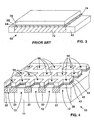
- FIG. 3 shows an isolation region of a prior art MOSFET device 60 with a doped silicon semiconductor substrate 62 on which an STI region 72 has been formed. Above the STI region is formed a gate conductor stack 74 of fill layers comprising a polysilicon layer 64, a silicide layer 68, and a silicon nitride gate insulator layer 70.
- Maskless STI (MSTI) Planarization for gate conductor Fill Technology is accomplished by designing the AA (active area) mask with dummy active silicon mesas within the holes of gate conductor punch-holes. These dummy active silicon mesas are designed with the same ground rules as the rest of the chip.
- Dash et al discusses STI planarization using polysilicon but differs from the present invention in several ways with respect to the level of the silicon oxide fill and the level of the polysilicon.
- the silicon oxide RIE used after polysilicon CMP does not include the required break-thru step and stops on the silicon nitride instead of in the silicon oxide. Both the break-thru step and having the RIE stop in the silicon oxide were found to be essential in creating a manufacturable process.
- a method for manufacture of a semiconductor FET device employing a Shallow Trench Isolation comprising the steps of: providing a doped silicon semiconductor substrate coated with a plurality of pad layer segments on the surface-of the substrate, and providing a patterned masking layer formed on said pad layer, which includes patterns for device mesas and dummy mesas, said dummy mesas being mesas that do not form active devices; forming raised active silicon device areas and dummy active silicon mesas said mesas having top surfaces capped with pad layer segments, said mesas being formed with said patterns from said doped silicon semiconductor substrate and said pad layer segments, said pad layer being below said patterned masking layer, then stripping said masking layer leaving said pad layer segments on said substrate; depositing a conformal blanket silicon oxide layer covering said doped silicon semiconductor substrate and said raised active silicon device areas and said dummy active silicon mesas with said mesas remaining capped with pad segments with conformal projections
- STI Shallow Trench Isolation
- the pad segments are stripped away from the device and then gate oxide layers are formed above the surfaces of the substrate exposed by stripping away the pad segments.
- P-wells and N-wells are formed in the substrate beneath the gate oxide layer and the silicon oxide layer.
- a step of blanket deposition of a gate conductor layer composed of a polysilicon sublayer and a silicide sublayer upon the device followed by blanket deposition of a dielectric layer, followed by patterning and etching of windows down to active device areas and dummy areas in the substrate followed by the step of formation of FET devices and dummy devices by ion implantation of a dose of source/drain dopant ions into the active device areas and the dummy areas in the P-wells and the N-wells.
- the pad structure is stripped from the device and a gate oxide layer is formed above the surface of the substrate exposed as the pad structure is stripped away.
- FET devices with gate structure are formed on the surface of the device with gate conductor structures and dummy structures formed on the surface of the planar silicon oxide layer.
- Gate Conductor (GC) stack Fill over trenches, and etch of the fill to produce vias for vertical contacts to diffusion areas on active sites.
- FIGS. 1A-1O illustrate a process of manufacturing a Shallow Trench Isolation (STI) device 10 in accordance with this invention.
- STI Shallow Trench Isolation
- FIG. 1A shows the device 10 in an early stage of manufacture.
- the device 10 is formed on a P-doped silicon substrate 11 upon which pad silicon dioxide/silicon nitride pad layer segments 14/14' have been formed.
- the silicon dioxide layer has a thickness from about 5nm to about 15nm and the silicon nitride layer has a thickness from about 100nm to about 150nm.
- the active area mask 15/15' has been formed on the surface of silicon nitride layer segments 14/14' to protect the pad silicon dioxide/silicon nitride pad layer segments 14/14' and the silicon mesas 12/12' formed from the substrate 11 beneath the mask 15/15' during etching of the pad layers 14/14' and etching shallow trenches 9/9'/9" in substrate 11 to a depth H below the surface of the pad layer segments 14/14'.
- the depth H is from about 350nm to about 480nm below the upper surface of the pad layer segments 14/14'.
- FIG. 1B shows the device 10 of FIG. 1A after the mask 15/15' has been stripped away from the device 10, leaving the substrate 11 with the raised (mesa) active areas 12, 12' covered with pad structures 14, 14'.
- the space between the pad structures 14, 14' is a width W from about 250nm to about 250 ⁇ m.
- FIG. 1C shows the device 10 of FIG. 1B after deposition of a silicon dioxide layer 22 (having a thickness from about 480nm to about 560nm) on the device 10 covering the shallow trenches 9/9'/9" and the pad layer segments 14/14' and the mesas 12/12'.
- a silicon dioxide layer 22 having a thickness from about 480nm to about 560nm
- the silicon dioxide layer 22 on device 10 is covered by deposition of a blanket polysilicon layer 24 on silicon oxide layer 22.
- Layer 24 has a thickness from about 400nm to about 480nm.
- FIG. 1D shows the device 10 of FIG. 1C after CMP (Chemical Mechanical) Polishing of blanket polysilicon layer 24 down to those portions of silicon dioxide layer 22 which are exposed because they overlie the remaining portions of the pad layer segments 14/14' above the mesas 12/12'.
- CMP Chemical Mechanical Polishing
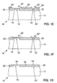
- FIG. 1E shows the device 10 of FIG. 1D after selective RIE partial etching of the exposed surface of the silicon dioxide layer 22 forming hollows 22' and 22" above the pad layer segments 14/14' above the mesas 12/12'.
- the etching removes a thickness from about 320nm to about 470nm of the silicon dioxide layer 22 over the remaining areas of pad layer 14/14'.
- FIG. 1F shows the device 10 of FIG. 1E after removal of the remainder of the polysilicon layer 24 with a selective etchant which removes the polysilicon layer 24 while leaving the silicon dioxide structure 22 with hollows 22'/22" intact. In this case a thickness from about 20nm to about 430nm of polysilicon layer 24 is removed.
- FIG. 1G shows the device 10 of FIG. 1F after a CMP process was used for about 50 seconds to about 70 seconds planarizing silicon dioxide layer 22 and clearing away the silicon nitride portion of pad layer 14/14'.
- the CMP process leaves the surface of device 10 as a planarized surface of silicon dioxide layer 22.
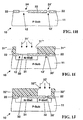
- FIG. 1H shows the device 10 of FIG. 1G after the silicon nitride and the silicon dioxide layers of the pad layer 14/14' have been stripped from device 10 leaving openings 24/24' in planar silicon dioxide layer 22 down to the surfaces of the mesas 12/12' exposed between the remaining portions of the silicon dioxide layer 22.
- FIG. 1I shows the device 10 of FIG. 1H after "gate" sacrificial silicon dioxide gate segments 30/30' about 12.5nm thick have been formed above the mesas. 12/12' by the conventional process of oxidation of the exposed surface of the substrate 11. Then V T implants are made through the sacrificial silicon dioxide gate segments 30/30' into the substrate 11.
- an N-well mask 31" has been formed over the device 11 with a N-well window 31' ' ' over the sacrificial silicon dioxide gate segments 30/30' through which N type dopant ions 31' are ion implanted into the surface of substrate 11 below the gate segment 30 to form an N-well 31.
- FIG. 1J shows the device 10 of FIG. 1I after N-well mask 31" has been stripped away and a P-well mask 32" has been formed over the device 11 with a P-well window 32''' over the sacrificial silicon oxide gate segment 30' through which P type dopant ions 32' are ion implanted into the surface of substrate 11 below the gate segment 30 forming a P-well region 32.
- FIG. 1K shows the device 10 of FIG. 1J after the sacrificial silicon oxide gate segments 30/30' have been stripped away by etching which also thins the silicon dioxide layer 22 to be coplanar with the surface of device 11. Then conventional gate silicon oxide (gate oxide) layer segments 38/38' (about 10nm thick) are formed on the surface of the mesas 12/12' within the recently enlarged openings 24/24'.
- gate oxide gate oxide
- FIG. 1L shows the device 10 of FIG. 1K after the planar oxide layer 22' and the gate oxide layer segments 38/38' have been coated with a doped polysilicon layer 40 preferably about 100nm thick, with a thickness range from about 50nm to about 100nm.
- Polysilicon layer 40 is coated with a silicide layer 42 preferably a tungsten silicide layer about 80nm thick, with a thickness range from about 50nm to about 200nm.
- Tungsten silicide layer 42 is coated with a silicon dioxide or silicon nitride gate insulator layer 44 preferably about 280nm thick, with a thickness range from about 200nm to about 400nm.
- the device is coated with a photoresist gate stack mask 46 with openings 48A, 48B therethrough over the ends of gate oxide layer segment 38 N-well and opening 48C therethrough over P-well 36.
- FIG. 1M shows the device 10 of FIG. 1L after the introduction of RIE etchant through openings 48A, 48B, and 48C down through gate insulator layer 44 etching openings 50A, 50B, and 50C therein extending down through tungsten silicide layer 42 and doped polysilicon layer 40 to expose the surface of the gate oxide layer segments 38/38' leaving a gate conductor stack 51 over N-well 34 with source/drain windows on either side and a dummy window 50C exposing the P-well for ion implanting subsequently.
- FIG. 1N shows the device 10 of FIG. 1M after ion implanting the P+ dopant source/drain regions 56S/56D below the silicon oxide segment 38 self-aligned with the gate conductor stack 51.
- FIG. 1O shows the device 10 of FIG. 1N after ion implanting the P+ dopant regions 58.
- MSTI maskless STI
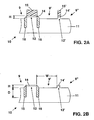
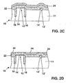
- FIGS. 2A-2G illustrate a process of manufacturing a Shallow Trench Isolation (STI) device 10 in accordance with this invention with deep trench capacitor structures 16.
- STI Shallow Trench Isolation
- FIG. 4 shows a perspective, sectional view of a portion of the device 10 in accordance with this invention with a dummy area in which the vias 54 reach down into dummy regions where no active devices have been formed.
- the structure is otherwise the same as the device described in FIGS. 1A-1O.
- the device 10 is formed on the P-doped silicon substrate 11 upon which silicon mesas 12 have been formed from the substrate 11 between the recesses therein containing the shallow trenches filled with the silicon oxide regions 22 upon which dummy gate conductor stacks of polysilicon layer 40, silicide layer 42 and the silicon dioxide or silicon nitride dielectric layer 44 have been formed. Between the dummy conductor stacks are the vias 54 (punch holes) which extend down to the top of the mesas 12.
- LOCOS is inexpensive but suffers from insulator thinning at narrow dimensions, bird's beak formation, field-implant encroachment, and creates significant wafer topography.
- Poly-Buffered LOCOS and Poly-encapsulated LOCOS improved the bird's beak formation but still result in a narrow channel effect that increases device vts.
- Shallow Trench Isolation provides an abrupt active-to-isolation transition without bird's beak formation with a minimum impact on device characteristics or topography.
- the process often requires extensive measurements and wafer to wafer process customization to control, i.e., a resist planarization mask used for fabrication of a 16Mb DRAM, and has a higher cost than LOCOS based methods.
- a manufacturable STI planarization process using Self-Aligned polysilicon and a planarization mask provides a stable and reliable process with a robust process window. It does not require extensive inline measurements or wafer to wafer process customization to control.
- the Self-Aligned Poly-silicon planarization process can be greatly simplified by use of mesas of active silicon within the STI regions in accordance with this invention.
- the cost has been calculated to decrease from about $145 to about $117 for the STI planarization module using MSTI.
- MSTI By designing active silicon mesas within large STI regions (within the gate conductor stack-Fill punch-hole areas in a gate conductor stack-Fill technology) and limiting the largest STI width to the planarization distance of CMP pad used for polishing the sacrificial polysilicon ( ⁇ 30 - 50 ⁇ m for an IC1000 CMP pad), MSTI can be easily implemented.
- GC gate conductor
Landscapes
- Element Separation (AREA)
- Insulated Gate Type Field-Effect Transistor (AREA)
- Weting (AREA)
- Metal-Oxide And Bipolar Metal-Oxide Semiconductor Integrated Circuits (AREA)
- Mechanical Treatment Of Semiconductor (AREA)
- Semiconductor Memories (AREA)
Description
- This invention relates to semiconductor devices and more particularly to shallow trench isolation in self-aligned FET devices.
- IBM Technical Disclosure Bulletin, vol.18, no. 6, pp 1753-4, November 1975 discloses a process for the manufacture of CMOS integrated circuit devices.
- European Patent Application 0 341 898 A discloses an improved method of planarization of topologies in integrated circuit structures.
- Conventional STI (Shallow Trench Isolation) planarization methods require a planarization mask, extensive measurements, and wafer-to-wafer process customization.
- Maskless STI Planarization using Self-Aligned Polysilicon process allows STI to be planarized without a planarization mask, with minimal measurements, without the need for wafer to wafer customization and can be designed to be completely ground rule compatible with a gate conductor stack Fill technology.
- United States patent No. 5,173,439 of Dash et al for "Forming Wide Dielectric-Filled Isolation Trenches In Semi-conductors" shows isolation trenches formed in pad silicon nitride/Si, followed by a silicon oxide layer, followed by a polysilicon layer, followed by Chemical Mechanical Polishing (CMP); followed by silicon oxide RIE (Reactive Ion Etching); followed by CMP down to a pad silicon nitride layer.
- U.S. patent No. 5,504,033 of Bajor et al for "Method for Forming Recessed Oxide Isolation Containing Deep And Shallow Trenches" describes in a fifth embodiment, after isolation trenches are dug into silicon nitride over silicon oxide over silicon, the trenches along with horizontal surfaces are first layered with silicon oxide, then sequentially a polysilicon layer; is followed by CMP. This reference appears not to address selective RIE partial silicon oxide etch over pad areas.
- United States patent No. 5,411,913 of Bashir et al for "Simple Planarized Trench Isolation and Field Oxide Formation using Poly-silicon" describes a process where after trenches are dug into pad silicon oxide/silicon nitride and into silicon; a layer of silicon oxide is deposited, followed by a layer of polysilicon, followed by RIE etch back to planarize. This reference appears not to address CMP polishing down to the silicon oxide layer and selective RIE partial silicon oxide etching over pad areas.
- United States patent No. 5,492,858 of Bose et al for "Shallow Trench Isolation Process Method for High Aspect Ratio Trenches" describes a process in which, after isolation trenches are dug through the pad silicon oxide/silicon nitride into silicon, a layer of silicon oxide is deposited and CMP etched back to silicon nitride to provide a planar surface for "active mesa sites." Bose et al. does not address deposition of polysilicon on a silicon oxide layer; CMP polishing down to the silicon oxide layer; and selective RIE partial silicon oxide etching over pad areas.
- United States patent No. 5,494,857 of Cooperman et al for "Chemical Mechanical Planarization of Shallow Trenches in Semiconductor Substrates" describes a process where, after trenches are dug in through pad silicon nitride/silicon oxide, a first silicon oxide layer is deposited, followed by a first silicon etch stop layer, followed by a second silicon oxide layer; followed by a CMP down to pad silicon nitride.
- United States patent No. 5,252,517 of Blalock et al for "Method of Conductor Isolation From A Conductive Contact Plug", describes a process where, after transistors are completed, a "planarizing insulator layer" is deposited and contact vias are etched down to diffusion areas and filled with polysilicon.
- United States patent No. 5,358,884 of Violette for "Dual Purpose Contact Collector Contact and Isolation Scheme for Advanced BICMOS Processes" shows trenches are dug through silicon nitride into silicon. Silicon oxide is deposited upon the silicon nitride, and CMP is done down to silicon nitride to create a "plurality of mesas."
- FIG. 3 shows an isolation region of a prior
art MOSFET device 60 with a dopedsilicon semiconductor substrate 62 on which anSTI region 72 has been formed. Above the STI region is formed agate conductor stack 74 of fill layers comprising a polysilicon layer 64, asilicide layer 68, and a silicon nitridegate insulator layer 70. - Maskless STI (MSTI) Planarization for gate conductor Fill Technology is accomplished by designing the AA (active area) mask with dummy active silicon mesas within the holes of gate conductor punch-holes. These dummy active silicon mesas are designed with the same ground rules as the rest of the chip.
- Dash et al discusses STI planarization using polysilicon but differs from the present invention in several ways with respect to the level of the silicon oxide fill and the level of the polysilicon. The silicon oxide RIE used after polysilicon CMP does not include the required break-thru step and stops on the silicon nitride instead of in the silicon oxide. Both the break-thru step and having the RIE stop in the silicon oxide were found to be essential in creating a manufacturable process.
- None of the patents discussed above describes the active area (AA) fill concept.
- In accordance with this invention, a method is provided for manufacture of a semiconductor FET device employing a Shallow Trench Isolation (STI) comprising the steps of: providing a doped silicon semiconductor substrate coated with a plurality of pad layer segments on the surface-of the substrate, and providing a patterned masking layer formed on said pad layer, which includes patterns for device mesas and dummy mesas, said dummy mesas being mesas that do not form active devices; forming raised active silicon device areas and dummy active silicon mesas said mesas having top surfaces capped with pad layer segments, said mesas being formed with said patterns from said doped silicon semiconductor substrate and said pad layer segments, said pad layer being below said patterned masking layer, then stripping said masking layer leaving said pad layer segments on said substrate; depositing a conformal blanket silicon oxide layer covering said doped silicon semiconductor substrate and said raised active silicon device areas and said dummy active silicon mesas with said mesas remaining capped with pad segments with conformal projections of said blanket silicon oxide layer above said mesas; depositing a conformal blanket sacrificial layer on said blanket silicon oxide layer with additional conformal projections of said sacrificial layer above said mesas; initially planarise said blanket sacrificial layer to remove said additional conformal projections until said silicon oxide layer is exposed only over said pad segments; selectively RIE etching said blanket conformal silicon oxide layer partially, over said mesas; selectively etch away the remainder of said sacrificial layer; perform later planarizing of said conformal blanket silicon oxide layer, leaving said conformal blanket silicon oxide layer at a level above said top surface of said mesas and then remove said pad segments forming openings in said conformal blanket silicon dioxide layer, exposing top surfaces of said active silicon device mesas and top surfaces of said dummy active silicon mesas below said openings, next form a conventional gate oxide layer on said surface of said device mesas and said dummy mesas; form a gate conductor stack for said FET device with source/drain openings therethrough self-aligned with said gate conductor stack over said active silicon device mesas; and then form an FET device and a dummy doped region in said dummy active silicon device mesa by implantation of a dose of source/drain dopant ions into said active device areas and said dummy areas in said semiconductor substrate. Preferably, the pad segments are composed of silicon nitride; or the pad segments are composed of a lower layer of silicon oxide capped with an upper layer of silicon nitride.
- It is also preferred that after the second chemical mechanical polishing, the pad segments are stripped away from the device and then gate oxide layers are formed above the surfaces of the substrate exposed by stripping away the pad segments.
- In addition, after formation of the gate oxide layer P-wells and N-wells are formed in the substrate beneath the gate oxide layer and the silicon oxide layer.
- Following formation of the wells there is a step of blanket deposition of a gate conductor layer composed of a polysilicon sublayer and a silicide sublayer upon the device followed by blanket deposition of a dielectric layer, followed by patterning and etching of windows down to active device areas and dummy areas in the substrate followed by the step of formation of FET devices and dummy devices by ion implantation of a dose of source/drain dopant ions into the active device areas and the dummy areas in the P-wells and the N-wells.
- Preferably, the pad structure is stripped from the device and a gate oxide layer is formed above the surface of the substrate exposed as the pad structure is stripped away.
- Preferably, FET devices with gate structure are formed on the surface of the device with gate conductor structures and dummy structures formed on the surface of the planar silicon oxide layer.
- "Gate Conductor (GC) stack Fill" over trenches, and etch of the fill to produce vias for vertical contacts to diffusion areas on active sites.
- The invention will now be described, by way of example only, with reference to the accompanying drawings, in which:
- FIGS. 1A-1O illustrate a process of manufacturing a Shallow Trench Isolation (STI) device in accordance with this invention.
- FIGS. 2A-2G illustrate a process of manufacturing a Shallow Trench Isolation (STI) device in accordance with this invention with deep trench capacitor structures.
- FIG. 3 shows an isolation region of a prior art MOSFET device.
- FIG. 4 shows a perspective view of the device in accordance with this invention with a dummy area in which the vias reach down into dummy regions where no active devices have been formed. The structure is otherwise the same as the device described in FIGS. 1A-1O.
-
- FIGS. 1A-1O illustrate a process of manufacturing a Shallow Trench Isolation (STI)
device 10 in accordance with this invention. - FIG. 1A shows the
device 10 in an early stage of manufacture. Thedevice 10 is formed on a P-dopedsilicon substrate 11 upon which pad silicon dioxide/silicon nitridepad layer segments 14/14' have been formed. In the pad layers segments 14/14' the silicon dioxide layer has a thickness from about 5nm to about 15nm and the silicon nitride layer has a thickness from about 100nm to about 150nm. Theactive area mask 15/15' has been formed on the surface of siliconnitride layer segments 14/14' to protect the pad silicon dioxide/silicon nitridepad layer segments 14/14' and thesilicon mesas 12/12' formed from thesubstrate 11 beneath themask 15/15' during etching of thepad layers 14/14' and etchingshallow trenches 9/9'/9" insubstrate 11 to a depth H below the surface of thepad layer segments 14/14'. The depth H is from about 350nm to about 480nm below the upper surface of thepad layer segments 14/14'. - FIG. 1B shows the
device 10 of FIG. 1A after themask 15/15' has been stripped away from thedevice 10, leaving thesubstrate 11 with the raised (mesa)active areas 12, 12' covered withpad structures 14, 14'. The space between thepad structures 14, 14' is a width W from about 250nm to about 250µm. - FIG. 1C shows the
device 10 of FIG. 1B after deposition of a silicon dioxide layer 22 (having a thickness from about 480nm to about 560nm) on thedevice 10 covering theshallow trenches 9/9'/9" and thepad layer segments 14/14' and themesas 12/12'. Next thesilicon dioxide layer 22 ondevice 10 is covered by deposition of ablanket polysilicon layer 24 onsilicon oxide layer 22.Layer 24 has a thickness from about 400nm to about 480nm. - FIG. 1D shows the
device 10 of FIG. 1C after CMP (Chemical Mechanical) Polishing ofblanket polysilicon layer 24 down to those portions ofsilicon dioxide layer 22 which are exposed because they overlie the remaining portions of thepad layer segments 14/14' above themesas 12/12'. - FIG. 1E shows the
device 10 of FIG. 1D after selective RIE partial etching of the exposed surface of thesilicon dioxide layer 22 forminghollows pad layer segments 14/14' above themesas 12/12'. The etching removes a thickness from about 320nm to about 470nm of thesilicon dioxide layer 22 over the remaining areas ofpad layer 14/14'. - FIG. 1F shows the
device 10 of FIG. 1E after removal of the remainder of thepolysilicon layer 24 with a selective etchant which removes thepolysilicon layer 24 while leaving thesilicon dioxide structure 22 withhollows 22'/22" intact. In this case a thickness from about 20nm to about 430nm ofpolysilicon layer 24 is removed. - FIG. 1G shows the
device 10 of FIG. 1F after a CMP process was used for about 50 seconds to about 70 seconds planarizingsilicon dioxide layer 22 and clearing away the silicon nitride portion ofpad layer 14/14'. Thus the CMP process leaves the surface ofdevice 10 as a planarized surface ofsilicon dioxide layer 22. - FIG. 1H shows the
device 10 of FIG. 1G after the silicon nitride and the silicon dioxide layers of thepad layer 14/14' have been stripped fromdevice 10 leavingopenings 24/24' in planarsilicon dioxide layer 22 down to the surfaces of themesas 12/12' exposed between the remaining portions of thesilicon dioxide layer 22. - FIG. 1I shows the
device 10 of FIG. 1H after "gate" sacrificial silicondioxide gate segments 30/30' about 12.5nm thick have been formed above the mesas. 12/12' by the conventional process of oxidation of the exposed surface of thesubstrate 11. Then VT implants are made through the sacrificial silicondioxide gate segments 30/30' into thesubstrate 11. - In addition, an N-
well mask 31" has been formed over thedevice 11 with a N-well window 31' ' ' over the sacrificial silicondioxide gate segments 30/30' through which N type dopant ions 31' are ion implanted into the surface ofsubstrate 11 below thegate segment 30 to form an N-well 31. - FIG. 1J shows the
device 10 of FIG. 1I after N-well mask 31" has been stripped away and a P-well mask 32" has been formed over thedevice 11 with a P-well window 32''' over the sacrificial silicon oxide gate segment 30' through which P type dopant ions 32' are ion implanted into the surface ofsubstrate 11 below thegate segment 30 forming a P-well region 32. - FIG. 1K shows the
device 10 of FIG. 1J after the sacrificial siliconoxide gate segments 30/30' have been stripped away by etching which also thins thesilicon dioxide layer 22 to be coplanar with the surface ofdevice 11. Then conventional gate silicon oxide (gate oxide)layer segments 38/38' (about 10nm thick) are formed on the surface of themesas 12/12' within the recentlyenlarged openings 24/24'. - FIG. 1L shows the
device 10 of FIG. 1K after theplanar oxide layer 22' and the gateoxide layer segments 38/38' have been coated with a dopedpolysilicon layer 40 preferably about 100nm thick, with a thickness range from about 50nm to about 100nm.Polysilicon layer 40 is coated with asilicide layer 42 preferably a tungsten silicide layer about 80nm thick, with a thickness range from about 50nm to about 200nm.Tungsten silicide layer 42 is coated with a silicon dioxide or silicon nitridegate insulator layer 44 preferably about 280nm thick, with a thickness range from about 200nm to about 400nm. - Next, the device is coated with a photoresist
gate stack mask 46 withopenings opening 48C therethrough over P-well 36. - FIG. 1M shows the
device 10 of FIG. 1L after the introduction of RIE etchant throughopenings gate insulator layer 44etching openings tungsten silicide layer 42 and dopedpolysilicon layer 40 to expose the surface of the gateoxide layer segments 38/38' leaving agate conductor stack 51 over N-well 34 with source/drain windows on either side and adummy window 50C exposing the P-well for ion implanting subsequently. - FIG. 1N shows the
device 10 of FIG. 1M after ion implanting the P+ dopant source/drain regions 56S/56D below thesilicon oxide segment 38 self-aligned with thegate conductor stack 51. - FIG. 1O shows the
device 10 of FIG. 1N after ion implanting theP+ dopant regions 58. - By designing dummy active silicon mesas in STI regions within the gate conductor stack by filling punch-hole areas, a maskless STI (MSTI) planarization process previously can be realized on products incorporating STI and gate conductor stack Fill technologies.
- FIGS. 2A-2G illustrate a process of manufacturing a Shallow Trench Isolation (STI)
device 10 in accordance with this invention with deeptrench capacitor structures 16. Corresponding structures in FIGS. 2A-2G are the same as those in FIGS. 1A-1G and the descriptions thereof apply to adevice 10 which includes the deeptrench capacitor structures 16 initially at the beginning of the process of manufacture. - FIG. 4 shows a perspective, sectional view of a portion of the
device 10 in accordance with this invention with a dummy area in which thevias 54 reach down into dummy regions where no active devices have been formed. The structure is otherwise the same as the device described in FIGS. 1A-1O. Thedevice 10 is formed on the P-dopedsilicon substrate 11 upon which silicon mesas 12 have been formed from thesubstrate 11 between the recesses therein containing the shallow trenches filled with thesilicon oxide regions 22 upon which dummy gate conductor stacks ofpolysilicon layer 40,silicide layer 42 and the silicon dioxide or siliconnitride dielectric layer 44 have been formed. Between the dummy conductor stacks are the vias 54 (punch holes) which extend down to the top of themesas 12. - For the ideally scalable ULSI CMOS device, process control of the isolation technology is crucial. Device isolation needs to provide an abrupt active-to-isolation transition with sufficient isolation depth and to provide a planar wafer surface. This must be achieved with a wide process window at a low cost.
- Several alternative planarization techniques have been proposed. For example, LOCOS is inexpensive but suffers from insulator thinning at narrow dimensions, bird's beak formation, field-implant encroachment, and creates significant wafer topography. Poly-Buffered LOCOS and Poly-encapsulated LOCOS improved the bird's beak formation but still result in a narrow channel effect that increases device vts.
- Shallow Trench Isolation (STI) provides an abrupt active-to-isolation transition without bird's beak formation with a minimum impact on device characteristics or topography. However, the process often requires extensive measurements and wafer to wafer process customization to control, i.e., a resist planarization mask used for fabrication of a 16Mb DRAM, and has a higher cost than LOCOS based methods.
- A manufacturable STI planarization process using Self-Aligned polysilicon and a planarization mask provides a stable and reliable process with a robust process window. It does not require extensive inline measurements or wafer to wafer process customization to control.
- The Self-Aligned Poly-silicon planarization process can be greatly simplified by use of mesas of active silicon within the STI regions in accordance with this invention. This allows the planarization mask, CMP stop silicon oxide layer deposition, and the CMP stop silicon oxide layer etch to be completely eliminated. This is compatible with a gate conductor stack with fill technology by using a 'punch-hole' gate conductor stack mask. This allows large area STI regions to have active silicon mesas placed within the gate conductor stack-fill 'punch-hole' areas, thus creating additional polish stop areas to prevent CMP dishing in the STI regions during planarization.
-
- 1. Substrates start with an STI of depth "H" with maximum width W. "H" depends on device design requirements. "W" depends on planarization distance of CMP pad used for polishing sacrificial polysilicon (∼30-50 µm for an IC1000 CMP Pad);
- 2. STI shapes are designed to have active silicon mesas placed within the gate conductor stack-Fill "punch-hole" areas;
- 3. Deposition of silicon oxide layer to be planarized of thickness "H" + 25% Ox; over initial pad structure (e.g. silicon nitride):
- 4. Deposition of polysilicon sacrificial layer of thickness "H" over silicon oxide layer.
- 5. CMP polysilicon layer stopping on silicon oxide layer;
- 6. Using a combination of non-selective & selective silicon oxide/polysilicon RIE, etch the silicon oxide over the initial pad structure to be coplanar with the top of the silicon oxide in the large STI areas. The RIE will leave a thin layer of polysilicon over the STI regions;
- 7. Selectively strip remaining polysilicon.
- 8. CMP remaining silicon oxide down to initial pad structure.

-
- The cost has been calculated to decrease from about $145 to about $117 for the STI planarization module using MSTI.
- Much development effort was invested in creating a manufacturable STI planarization process using self-aligned polysilicon for this process. Data was collected and analyzed from hundreds of integrated product lots showing that the method of this invention for STI planarization creates a stable process with a large process window.
- Simplifying the self-aligned polysilicon STI planarization process by eliminating a planarization mask allows the polysilicon CMP stop silicon oxide layer and polysilicon CMP stop silicon oxide etch processes to be eliminated also.
- By designing active silicon mesas within large STI regions (within the gate conductor stack-Fill punch-hole areas in a gate conductor stack-Fill technology) and limiting the largest STI width to the planarization distance of CMP pad used for polishing the sacrificial polysilicon (~30 - 50 µm for an IC1000 CMP pad), MSTI can be easily implemented.
- There is a gate conductor (GC) stack with fill over trenches, and the fill is etched to produce vias for vertical contacts to diffusion areas on active sites.
Claims (8)
- A method of manufacture of a semiconductor FET device (10) employing a Shallow Trench Isolation (STI), the method comprising the steps of:a) providing a doped silicon semiconductor substrate (11) coated with a plurality of pad layer segments (14, 14') on the surface of the substrate, and providing a patterned masking layer (15, 15') formed on said pad layer, which includes patterns for device mesas and dummy mesas, said dummy mesas being mesas that do not form active devices;b) forming raised active silicon device areas and dummy active silicon mesas (12, 12'), said mesas having top surfaces capped with pad layer segments, said mesas being formed with said patterns from said doped silicon semiconductor substrate and said pad layer segments, said pad layer being below said patterned masking layer, then stripping said masking layer leaving said pad layer segments on said substrate;c) depositing a conformal blanket silicon oxide (22) layer covering said doped silicon semiconductor substrate and said raised active silicon device areas and said dummy active silicon mesas with said mesas remaining capped with pad segments with conformal projections of said blanket silicon oxide layer above said mesas;d) depositing a conformal blanket sacrificial layer (24) on said blanket silicon oxide layer with additional conformal projections of said sacrificial layer above said mesas;e) initially planarise said blanket sacrificial layer (24) to remove said additional conformal projections until said silicon oxide layer is exposed only over said pad segments;f) selectively RIE etching said blanket conformal silicon oxide layer (22) partially, over said mesas;g) selectively etch away the remainder of said sacrificial layer;h) perform later planarizing of said conformal blanket silicon oxide layer (22), leaving said conformal blanket silicon oxide layer at a level above said top surface of said mesas and then remove said pad segments forming openings (24, 24') in said conformal blanket silicon dioxide layer, exposing top surfaces of said active silicon device mesas and top surfaces of said dummy active silicon mesas below said openings;i) next form a conventional gate oxide layer (38, 38') on said surface of said device mesas and said dummy mesas;k) form a gate conductor stack (51) for said FET device with source/drain openings (50A, 50B) therethrough self-aligned with said gate conductor stack over said active silicon device mesas; andl) then form an FET device and a dummy doped region (58) in said dummy active silicon device mesa by implantation of a dose of source/drain dopant ions into said active device areas and said dummy areas in said semiconductor substrate.
- A method as claimed in claim 1 wherein said planarizing steps (e) and (h) comprise performing chemical mechanical polishing.
- A method as claimed in claim 1 or claim 2 wherein said pad segments (14) are composed of silicon nitride used as an etch stop in planarizing said silicon oxide layer (22) into a planar silicon oxide layer.
- A method as claimed in claim 1 or claim 2 wherein said pad segments (14) are composed of a lower layer of silicon oxide capped with an upper layer (14) of silicon nitride using said silicon nitride in said pad structure as an etch stop in planarizing said silicon oxide layer (22) into a planar silicon oxide layer.
- A method as claimed in claim 2 wherein the method further comprises the step of, after said chemical mechanical polishing in step (h), stripping away said pad segments from said device (10) and then forming gate oxide layers above the surfaces of said substrate exposed by stripping away said pad segments.
- A method as claimed in claim 5 wherein after formation of said gate oxide (38), layer P-wells (36) and N-wells (34) are formed in said substrate beneath said gate oxide layer and said silicon oxide layer (22).
- A method as claimed in claim 6 wherein following formation of said wells (36, 34) there is a step of blanket deposition of a gate conductor layer upon said device (10) followed by blanket deposition of a dielectric layer (40), followed by patterning and etching of windows down to active device areas and dummy areas in said substrate (11) followed by the step of formation of FET devices and dummy devices by ion implantation (56, 58) of a dose of source/drain dopant ions into said active device areas and said dummy areas in said P-wells (36) and said N-wells (34).
- A method as claimed in claim 6 wherein following formation of said wells (36, 34) there is a step of blanket deposition of a gate conductor layer composed of a polysilicon sublayer (40) and a silicide sublayer (42) upon said device (10) followed by blanket deposition of a dielectric layer (44), followed by patterning and etching of windows down to active device areas and dummy areas in said substrate followed by the step of formation of FET devices and dummy devices by ion implantation (56, 58) of a dose of source/drain dopant ions into said active device areas and said dummy areas in said P-wells (36) and said N-wells (34).
Applications Claiming Priority (2)
| Application Number | Priority Date | Filing Date | Title |
|---|---|---|---|
| US850093 | 1997-05-01 | ||
| US08/850,093 US6103592A (en) | 1997-05-01 | 1997-05-01 | Manufacturing self-aligned polysilicon fet devices isolated with maskless shallow trench isolation and gate conductor fill technology with active devices and dummy doped regions formed in mesas |
Publications (3)
| Publication Number | Publication Date |
|---|---|
| EP0875927A2 EP0875927A2 (en) | 1998-11-04 |
| EP0875927A3 EP0875927A3 (en) | 1999-07-07 |
| EP0875927B1 true EP0875927B1 (en) | 2004-06-16 |
Family
ID=25307239
Family Applications (1)
| Application Number | Title | Priority Date | Filing Date |
|---|---|---|---|
| EP98303125A Expired - Lifetime EP0875927B1 (en) | 1997-05-01 | 1998-04-23 | Method of manufacturing FET devices with maskless shallow trench isolation (STI) |
Country Status (4)
| Country | Link |
|---|---|
| US (1) | US6103592A (en) |
| EP (1) | EP0875927B1 (en) |
| JP (1) | JPH1126595A (en) |
| DE (1) | DE69824481T2 (en) |
Families Citing this family (36)
| Publication number | Priority date | Publication date | Assignee | Title |
|---|---|---|---|---|
| JP3638778B2 (en) * | 1997-03-31 | 2005-04-13 | 株式会社ルネサステクノロジ | Semiconductor integrated circuit device and manufacturing method thereof |
| US7001713B2 (en) * | 1998-04-18 | 2006-02-21 | United Microelectronics, Corp. | Method of forming partial reverse active mask |
| KR100272166B1 (en) * | 1998-06-30 | 2000-11-15 | 윤종용 | Semiconductor device having dummy conductive layer formed on isolation regio and manufacturing method thereof |
| US6432832B1 (en) * | 1999-06-30 | 2002-08-13 | Lam Research Corporation | Method of improving the profile angle between narrow and wide features |
| JP2001024280A (en) * | 1999-07-13 | 2001-01-26 | Oki Electric Ind Co Ltd | Semiconductor optical functional element |
| US6291307B1 (en) * | 1999-08-06 | 2001-09-18 | Chartered Semiconductor Manufacturing Ltd. | Method and structure to make planar analog capacitor on the top of a STI structure |
| US6180535B1 (en) * | 1999-09-03 | 2001-01-30 | Taiwan Semiconductors Manufacturing Company | Approach to the spacer etch process for CMOS image sensor |
| JP3415602B2 (en) * | 2000-06-26 | 2003-06-09 | 鹿児島日本電気株式会社 | Pattern formation method |
| US6355524B1 (en) * | 2000-08-15 | 2002-03-12 | Mosel Vitelic, Inc. | Nonvolatile memory structures and fabrication methods |
| US6559055B2 (en) | 2000-08-15 | 2003-05-06 | Mosel Vitelic, Inc. | Dummy structures that protect circuit elements during polishing |
| JP3719650B2 (en) * | 2000-12-22 | 2005-11-24 | 松下電器産業株式会社 | Semiconductor device |
| DE10123509A1 (en) * | 2001-05-15 | 2002-11-28 | Infineon Technologies Ag | Planarization of semiconductor structure involves providing second area on layer to be planarized that is continuously masked using pre-planarizing mask |
| US6753252B2 (en) | 2001-05-18 | 2004-06-22 | Infineon Technologies Ag | Contact plug formation for devices with stacked capacitors |
| US6475875B1 (en) | 2001-07-09 | 2002-11-05 | Chartered Semiconductor Manufacturing Ltd. | Shallow trench isolation elevation uniformity via insertion of a polysilicon etch layer |
| JP3418386B2 (en) * | 2001-08-16 | 2003-06-23 | 沖電気工業株式会社 | Method for manufacturing semiconductor device |
| KR100419872B1 (en) * | 2001-09-13 | 2004-02-25 | 주식회사 하이닉스반도체 | method for isolating semiconductor device |
| US6821847B2 (en) * | 2001-10-02 | 2004-11-23 | Mosel Vitelic, Inc. | Nonvolatile memory structures and fabrication methods |
| US6551922B1 (en) | 2002-03-06 | 2003-04-22 | Motorola, Inc. | Method for making a semiconductor device by variable chemical mechanical polish downforce |
| US6627510B1 (en) * | 2002-03-29 | 2003-09-30 | Sharp Laboratories Of America, Inc. | Method of making self-aligned shallow trench isolation |
| KR100474591B1 (en) | 2002-04-23 | 2005-03-08 | 주식회사 하이닉스반도체 | Method for fabricating dram cell transistor having trench isolation structure |
| US20040079974A1 (en) * | 2002-10-24 | 2004-04-29 | Texas Instruments Incorporated | Method for manufacturing a semiconductor device using dummy openings in a photoresist material and an LDMOS device manufactured in accordance with the method |
| US20050009312A1 (en) * | 2003-06-26 | 2005-01-13 | International Business Machines Corporation | Gate length proximity corrected device |
| US7432179B2 (en) * | 2004-12-15 | 2008-10-07 | Taiwan Semiconductor Manufacturing Company, Ltd. | Controlling gate formation by removing dummy gate structures |
| US7701034B2 (en) * | 2005-01-21 | 2010-04-20 | Taiwan Semiconductor Manufacturing Company, Ltd. | Dummy patterns in integrated circuit fabrication |
| DE102005004708B4 (en) * | 2005-02-02 | 2006-11-02 | Atmel Germany Gmbh | Method for producing integrated circuits with at least one silicon germanium heterobipolar transistor |
| US20060257790A1 (en) * | 2005-05-16 | 2006-11-16 | Taiwan Semiconductor Manufacturing Company, Ltd. | A semiconductor device structure and methods of manufacturing thereof |
| US7939384B2 (en) * | 2008-12-19 | 2011-05-10 | Taiwan Semiconductor Manufacturing Company, Ltd. | Eliminating poly uni-direction line-end shortening using second cut |
| US20120264300A1 (en) * | 2011-04-13 | 2012-10-18 | Nanya Technology Corporation | Method of fabricating semiconductor component |
| CN102347268B (en) * | 2011-10-28 | 2015-07-22 | 上海华虹宏力半导体制造有限公司 | Method for producing semiconductor device |
| FR2998417A1 (en) | 2012-11-16 | 2014-05-23 | St Microelectronics Rousset | METHOD FOR PRODUCING AN INTEGRATED CIRCUIT POINT ELEMENT, AND CORRESPONDING INTEGRATED CIRCUIT |
| KR20150021811A (en) * | 2013-08-21 | 2015-03-03 | 삼성전자주식회사 | Method of manufacturing the semiconductor device |
| US9202859B1 (en) | 2014-05-27 | 2015-12-01 | Texas Instruments Incorporated | Well resistors and polysilicon resistors |
| US10074721B2 (en) | 2016-09-22 | 2018-09-11 | Infineon Technologies Ag | Method of fabricating a semiconductor wafer that includes producing a planarised surface having both a mesa surface and an insulating layer surface |
| US10134603B2 (en) * | 2016-09-22 | 2018-11-20 | Infineon Technologies Ag | Method of planarising a surface |
| US10199271B1 (en) * | 2017-09-01 | 2019-02-05 | Globalfoundries Inc. | Self-aligned metal wire on contact structure and method for forming same |
| CN116001256B (en) * | 2022-12-27 | 2024-08-30 | 中国科学院光电技术研究所 | Maskless etching processing method for manufacturing binary optical element by special-shaped electrode |
Family Cites Families (13)
| Publication number | Priority date | Publication date | Assignee | Title |
|---|---|---|---|---|
| US4962064A (en) * | 1988-05-12 | 1990-10-09 | Advanced Micro Devices, Inc. | Method of planarization of topologies in integrated circuit structures |
| US5173439A (en) * | 1989-10-25 | 1992-12-22 | International Business Machines Corporation | Forming wide dielectric-filled isolation trenches in semi-conductors |
| EP0445471A3 (en) * | 1990-03-06 | 1994-10-26 | Digital Equipment Corp | Method of forming isolation trenches in a semiconductor substrate |
| US5077234A (en) * | 1990-06-29 | 1991-12-31 | Digital Equipment Corporation | Planarization process utilizing three resist layers |
| US5382541A (en) * | 1992-08-26 | 1995-01-17 | Harris Corporation | Method for forming recessed oxide isolation containing deep and shallow trenches |
| US5358884A (en) * | 1992-09-11 | 1994-10-25 | Micron Technology, Inc. | Dual purpose collector contact and isolation scheme for advanced bicmos processes |
| US5252517A (en) * | 1992-12-10 | 1993-10-12 | Micron Semiconductor, Inc. | Method of conductor isolation from a conductive contact plug |
| US5494857A (en) * | 1993-07-28 | 1996-02-27 | Digital Equipment Corporation | Chemical mechanical planarization of shallow trenches in semiconductor substrates |
| US5492858A (en) * | 1994-04-20 | 1996-02-20 | Digital Equipment Corporation | Shallow trench isolation process for high aspect ratio trenches |
| US5411913A (en) * | 1994-04-29 | 1995-05-02 | National Semiconductor Corporation | Simple planarized trench isolation and field oxide formation using poly-silicon |
| US5663107A (en) * | 1994-12-22 | 1997-09-02 | Siemens Aktiengesellschaft | Global planarization using self aligned polishing or spacer technique and isotropic etch process |
| US5773328A (en) * | 1995-02-28 | 1998-06-30 | Sgs-Thomson Microelectronics, Inc. | Method of making a fully-dielectric-isolated fet |
| US5721172A (en) * | 1996-12-02 | 1998-02-24 | Taiwan Semiconductor Manufacturing Company, Ltd. | Self-aligned polish stop layer hard masking method for forming planarized aperture fill layers |
-
1997
- 1997-05-01 US US08/850,093 patent/US6103592A/en not_active Expired - Fee Related
-
1998
- 1998-04-23 EP EP98303125A patent/EP0875927B1/en not_active Expired - Lifetime
- 1998-04-23 DE DE69824481T patent/DE69824481T2/en not_active Expired - Fee Related
- 1998-04-27 JP JP10116498A patent/JPH1126595A/en active Pending
Also Published As
| Publication number | Publication date |
|---|---|
| EP0875927A3 (en) | 1999-07-07 |
| DE69824481D1 (en) | 2004-07-22 |
| JPH1126595A (en) | 1999-01-29 |
| EP0875927A2 (en) | 1998-11-04 |
| US6103592A (en) | 2000-08-15 |
| DE69824481T2 (en) | 2005-07-07 |
Similar Documents
| Publication | Publication Date | Title |
|---|---|---|
| EP0875927A2 (en) | Method of manufacturing FET devices with maskless shallow trench isolation (STI) | |
| US5229316A (en) | Semiconductor processing method for forming substrate isolation trenches | |
| US6864152B1 (en) | Fabrication of trenches with multiple depths on the same substrate | |
| US6518641B2 (en) | Deep slit isolation with controlled void | |
| US6251734B1 (en) | Method for fabricating trench isolation and trench substrate contact | |
| EP1069613B1 (en) | Low-leakage architecture for sub-0.18 micrometer salicided CMOS device | |
| US5292683A (en) | Method of isolating semiconductor devices and arrays of memory integrated circuitry | |
| EP0782185B1 (en) | Process of fabricating semiconductor device having isolating oxide rising out of groove | |
| US7049206B2 (en) | Device isolation for semiconductor devices | |
| US6281082B1 (en) | Method to form MOS transistors with a common shallow trench isolation and interlevel dielectric gap fill | |
| US20030017710A1 (en) | Method to improve latchup by forming selective sloped staircase STI structure to use in the I/0 or latchup sensitive area | |
| US6225175B1 (en) | Process for defining ultra-thin geometries | |
| JP3215320B2 (en) | Method for manufacturing semiconductor device | |
| US6919612B2 (en) | Biasable isolation regions using epitaxially grown silicon between the isolation regions | |
| US7365400B2 (en) | Semiconductor device and method for manufacturing the same | |
| US6380088B1 (en) | Method to form a recessed source drain on a trench side wall with a replacement gate technique | |
| JP2861856B2 (en) | Method for manufacturing semiconductor device | |
| US6620663B1 (en) | Self-aligned copper plating/CMP process for RF lateral MOS device | |
| US6350638B2 (en) | Method of forming complementary type conductive regions on a substrate | |
| US7179713B2 (en) | Method of fabricating a fin transistor | |
| US6835641B1 (en) | Method of forming single sided conductor and semiconductor device having the same | |
| US6080625A (en) | Method for making dual-polysilicon structures in integrated circuits | |
| US6319795B1 (en) | Method for fabricating VLSI devices having trench isolation regions | |
| US5767000A (en) | Method of manufacturing subfield conductive layer | |
| US6239001B1 (en) | Method for making a semiconductor device |
Legal Events
| Date | Code | Title | Description |
|---|---|---|---|
| PUAI | Public reference made under article 153(3) epc to a published international application that has entered the european phase |
Free format text: ORIGINAL CODE: 0009012 |
|
| AK | Designated contracting states |
Kind code of ref document: A2 Designated state(s): DE FR GB |
|
| AX | Request for extension of the european patent |
Free format text: AL;LT;LV;MK;RO;SI |
|
| PUAL | Search report despatched |
Free format text: ORIGINAL CODE: 0009013 |
|
| AK | Designated contracting states |
Kind code of ref document: A3 Designated state(s): AT BE CH CY DE DK ES FI FR GB GR IE IT LI LU MC NL PT SE |
|
| AX | Request for extension of the european patent |
Free format text: AL;LT;LV;MK;RO;SI |
|
| 17P | Request for examination filed |
Effective date: 19991227 |
|
| AKX | Designation fees paid |
Free format text: DE FR GB |
|
| 17Q | First examination report despatched |
Effective date: 20011026 |
|
| GRAP | Despatch of communication of intention to grant a patent |
Free format text: ORIGINAL CODE: EPIDOSNIGR1 |
|
| GRAS | Grant fee paid |
Free format text: ORIGINAL CODE: EPIDOSNIGR3 |
|
| GRAA | (expected) grant |
Free format text: ORIGINAL CODE: 0009210 |
|
| AK | Designated contracting states |
Kind code of ref document: B1 Designated state(s): DE FR GB |
|
| REG | Reference to a national code |
Ref country code: GB Ref legal event code: FG4D |
|
| REF | Corresponds to: |
Ref document number: 69824481 Country of ref document: DE Date of ref document: 20040722 Kind code of ref document: P |
|
| ET | Fr: translation filed | ||
| PLBE | No opposition filed within time limit |
Free format text: ORIGINAL CODE: 0009261 |
|
| STAA | Information on the status of an ep patent application or granted ep patent |
Free format text: STATUS: NO OPPOSITION FILED WITHIN TIME LIMIT |
|
| PG25 | Lapsed in a contracting state [announced via postgrant information from national office to epo] |
Ref country code: GB Free format text: LAPSE BECAUSE OF NON-PAYMENT OF DUE FEES Effective date: 20050423 |
|
| 26N | No opposition filed |
Effective date: 20050317 |
|
| GBPC | Gb: european patent ceased through non-payment of renewal fee |
Effective date: 20050423 |
|
| PGFP | Annual fee paid to national office [announced via postgrant information from national office to epo] |
Ref country code: DE Payment date: 20080423 Year of fee payment: 11 |
|
| PG25 | Lapsed in a contracting state [announced via postgrant information from national office to epo] |
Ref country code: DE Free format text: LAPSE BECAUSE OF NON-PAYMENT OF DUE FEES Effective date: 20091103 |
|
| PGFP | Annual fee paid to national office [announced via postgrant information from national office to epo] |
Ref country code: FR Payment date: 20110420 Year of fee payment: 14 |
|
| REG | Reference to a national code |
Ref country code: FR Ref legal event code: ST Effective date: 20121228 |
|
| PG25 | Lapsed in a contracting state [announced via postgrant information from national office to epo] |
Ref country code: FR Free format text: LAPSE BECAUSE OF NON-PAYMENT OF DUE FEES Effective date: 20120430 |