EP0860098B1 - Circuit arrangement - Google Patents
Circuit arrangement Download PDFInfo
- Publication number
- EP0860098B1 EP0860098B1 EP97927320A EP97927320A EP0860098B1 EP 0860098 B1 EP0860098 B1 EP 0860098B1 EP 97927320 A EP97927320 A EP 97927320A EP 97927320 A EP97927320 A EP 97927320A EP 0860098 B1 EP0860098 B1 EP 0860098B1
- Authority
- EP
- European Patent Office
- Prior art keywords
- value
- signal
- comparator
- input terminal
- state
- Prior art date
- Legal status (The legal status is an assumption and is not a legal conclusion. Google has not performed a legal analysis and makes no representation as to the accuracy of the status listed.)
- Expired - Lifetime
Links
Images


Classifications
-
- H—ELECTRICITY
- H05—ELECTRIC TECHNIQUES NOT OTHERWISE PROVIDED FOR
- H05B—ELECTRIC HEATING; ELECTRIC LIGHT SOURCES NOT OTHERWISE PROVIDED FOR; CIRCUIT ARRANGEMENTS FOR ELECTRIC LIGHT SOURCES, IN GENERAL
- H05B41/00—Circuit arrangements or apparatus for igniting or operating discharge lamps
- H05B41/14—Circuit arrangements
- H05B41/26—Circuit arrangements in which the lamp is fed by power derived from dc by means of a converter, e.g. by high-voltage dc
- H05B41/28—Circuit arrangements in which the lamp is fed by power derived from dc by means of a converter, e.g. by high-voltage dc using static converters
- H05B41/282—Circuit arrangements in which the lamp is fed by power derived from dc by means of a converter, e.g. by high-voltage dc using static converters with semiconductor devices
- H05B41/285—Arrangements for protecting lamps or circuits against abnormal operating conditions
- H05B41/2851—Arrangements for protecting lamps or circuits against abnormal operating conditions for protecting the circuit against abnormal operating conditions
- H05B41/2855—Arrangements for protecting lamps or circuits against abnormal operating conditions for protecting the circuit against abnormal operating conditions against abnormal lamp operating conditions
-
- Y—GENERAL TAGGING OF NEW TECHNOLOGICAL DEVELOPMENTS; GENERAL TAGGING OF CROSS-SECTIONAL TECHNOLOGIES SPANNING OVER SEVERAL SECTIONS OF THE IPC; TECHNICAL SUBJECTS COVERED BY FORMER USPC CROSS-REFERENCE ART COLLECTIONS [XRACs] AND DIGESTS
- Y02—TECHNOLOGIES OR APPLICATIONS FOR MITIGATION OR ADAPTATION AGAINST CLIMATE CHANGE
- Y02B—CLIMATE CHANGE MITIGATION TECHNOLOGIES RELATED TO BUILDINGS, e.g. HOUSING, HOUSE APPLIANCES OR RELATED END-USER APPLICATIONS
- Y02B20/00—Energy efficient lighting technologies, e.g. halogen lamps or gas discharge lamps
Definitions
- the invention relates to a circuit arrangement for operating a discharge lamp, provided with
- the signal S in the known circuit arrangement which is a measure for a value of an operating parameter is a signal which is a measure for the current through the discharge lamp (also referred to as lamp hereinafter).
- the control circuit achieves that the amplitude of the current through the lamp remains approximately constant. It is also possible to choose an alternative operating parameter such as, for example, the voltage across the lamp. If, for example, the discharge lamp fails to ignite after the circuit arrangement has been switched on, the voltage across the discharge lamp will rise to the point where the internal signal S int exceeds the value of the first internal reference signal. This activates the means III.
- the means III effect a change in the operating state of the means I such that this causes the voltage across the discharge lamp to drop.
- the voltage across the discharge lamp is not maintained at a high value by the circuit arrangement for a long period if the discharge lamp should fail to ignite. It is desirable in many cases not only to provide measures which ensure that the value of an operating parameter does not exceed a maximum admissible value (for a long period), but also to ensure that the same operating parameter cannot assume an undesirably low value. If the operating parameter is the voltage across the discharge lamp, a (too) low value of this voltage may point to a (too) high value of the current through the discharge lamp or a defect in a capacitor connected parallel to the discharge lamp.
- control circuit such that the means II are coupled to only one input terminal of the integrated circuit, and that one and the same signal S int is compared with a first internal reference signal and with a second internal reference signal. Such a construction of the control circuit, however, renders it necessary to lay down the relationship between the two internal reference signals in the integrated circuit.
- the relationship between the two reference values for example the relationship between the minimum admissible value and the maximum admissible value of the operating parameter, is then also laid down in such a construction of the control circuit.
- the minimum admissible value and the maximum admissible value of an operating parameter such as the voltage across the discharge lamp, however, are generally speaking dependent on specific properties of the discharge lamp and of the construction of the circuit arrangement. It is desirable for this reason to have a possibility of setting these reference values independently of one another.
- This is possible through the use of two input terminals of the integrated circuit. These two input terminals are coupled to the means II in that case, and each of the input terminals is coupled to comparator means and means for generating a reference signal.
- Such a solution requires a comparatively large number of input terminals, which renders the integrated circuit large and expensive.
- this solution often requires a comparatively large number of external components, so that the circuit arrangement becomes complicated and expensive.
- the invention has for its object to provide a circuit arrangement of the kind mentioned in the opening paragraph with which it is possible to adjust two reference values of the signal S independently of one another, while the means II are coupled to only one input terminal.
- a circuit arrangement of the kind mentioned in the opening paragraph is for this purpose characterized in that the means II are coupled to the input terminal T via an impedance P, and in that the integrated circuit is in addition provided with
- the comparator means Comp are in the first state when the amplitude of the electrical quantity G has the first value, in which case the internal signal S int is compared with the first internal reference signal. This means that the signal S is compared with a first reference value derived from the first internal reference signal. If the amplitude of the electrical quantity G has the second value, the internal signal S int is compared with the second internal reference signal. This means that the signal S is compared with a second reference value derived from the second internal reference signal.
- the first and the second internal reference signal have been laid down in the integrated circuit, it is possible to adjust the first and the second reference value independently of one another by means of the impedance value of impedance P and the dimensioning of the means II.
- the means III change the operational state of the means I whenever the signal S has passed one of these reference values.
- the electrical quantity G may be the voltage present at the input terminal T, in which case the means IV are provided with means for changing the amplitude of the voltage present at the input terminal from a first value V1 to a second value V2.
- the second value V2 is chosen to be zero.
- the integrated circuit may be of a comparatively simple construction in that case.
- the electrical quantity G may alternatively be the current flowing through the input terminal.
- the means IV are provided with means for changing the amplitude of the current flowing through the input terminal from a first value I1 to a second value I2.
- the means IV may comprise a first current source and a second current source, the first current source supplying a current whose amplitude is equal to the first value I1 and the second current source supplying a current whose amplitude is equal to the second value 12.
- the second value I2 is chosen to be zero.
- the integrated circuit can be of a comparatively simple construction then.
- the means IV are provided with means IVa for periodically changing the amplitude of the electrical quantity G from the first value to the second value and vice versa with a frequency f and for periodically changing the operational state of the comparator means Comp from the first state to the second state and vice versa. It is possible in that case to repeat the comparison of the signal S with the reference values continuously and thus to monitor the relevant operating parameter during a longer period.
- the means I comprise at least a switching element and means IVb for rendering the switching element conducting and non-conducting during lamp operation
- the frequency with which the switching element is rendered conducting and non-conducting is preferably chosen to be equal to the frequency f, and the changes in amplitude of the electrical quantity G and in the operational state of the comparator means Comp take place in synchronity with the cycle in which the switching element is rendered conducting and non-conducting:
- a comparatively simple construction of the integrated circuit is possible if the first internal reference signal is equal to the second internal reference signal, and the means D are formed by the means C.
- K1 and K2 form input terminals for coupling to a supply voltage source.
- Circuit portion I in this embodiment forms means I coupled to the input terminals for generating a current through the discharge lamp from a supply voltage delivered by the supply voltage source.
- the current through the discharge lamp is a high-frequency alternating current in this embodiment.
- a discharge lamp La is connected to respective output terminals of the means I.
- Ohmic resistors R1 and R2 together with circuit portion IIa form means II in this embodiment for generating a signal S which is a measure for the value of an operating parameter.
- the operating parameter is the amplitude of the AC voltage present across the discharge lamp La during lamp operation in this embodiment.
- Circuit portion IIa may comprise, for example, means for generating a DC voltage signal which is a measure for the rms value of the voltage across the discharge lamp. Another possibility is that circuit portion . IIa comprises means for generating a DC voltage signal which is a measure for the sum of the amplitudes of the voltages across the discharge lamp in both directions.
- Ohmic resistor P in this embodiment forms an impedance P.
- the other circuit portions and components shown in Fig. 1 together form an integrated circuit IC.
- T is an input terminal of the integrated circuit IC which is coupled to the means II via ohmic resistor P.
- Circuit portion IVa together with switching element Sw1 and switching element Sw2 forms means IV and at the same time means for periodically changing the amplitude of an electrical quantity G present at the input terminal from a first to a second value and vice versa and for changing the operational state of the comparator means Comp from a first state to a second state, said comparator means Comp comparing an internal signal S int with a first internal reference signal in the first state and comparing the internal signal S int with a second internal reference signal in the second state.
- the quantity G present at the input terminal in this embodiment is formed by the voltage applied to the input terminal, having a first value V1 and a second value V2.
- A, B, C and D are circuit portions for generating, in that order, a voltage whose amplitude is equal to the first value V1, a voltage whose amplitude is equal to the second value V2, a voltage which in this embodiment forms the first internal reference signal, and a voltage which in this embodiment forms the second reference signal.
- the integrated circuit IC comprises a circuit portion E, two comparators Comp1 and Comp2, and a circuit portion III which in this embodiment forms the means III for changing the operational state of the means I when the signal S has passed a reference value which is derived from the internal reference signal.
- the circuit portion E in this embodiment forms means E for generating the internal signal S int which is derived from the signal S.
- the comparators Comp1 and Comp2 in this embodiment form the comparator means Comp.
- Ends of the discharge lamp La are connected to respective inputs of circuit portion lla.
- a first output of circuit portion lla is connected to a second output by means of a series circuit of ohmic resistor R1 and ohmic resistor R2.
- a common junction point of ohmic resistor R1 and ohmic resistor R2 is connected to terminal Ts.
- Terminal Ts is connected to input terminal T via ohmic resistor P.
- Input terminal T is connected to a first main electrode of switching element Sw1.
- a second and a third main electrode of switching element Sw1 are connected to an output of circuit portion A and an output of circuit portion B, respectively.
- E is a circuit portion for generating a voltage which is proportional to the current through the input terminal T.
- An input of circuit portion E is for this purpose coupled to input terminal T.
- An output of circuit portion E is connected to a first main electrode of switching element Sw2.
- a second and a third main electrode of switching element Sw2 are connected to an input of comparator Comp1 and to an input of comparator Comp2, respectively.
- a further input of comparator Comp1 is connected to an output of circuit portion C, and a further input of comparator Comp2 is connected to an output of circuit portion D.
- Outputs of the circuit portion IVa are coupled to respective control electrodes of switching elements Sw1 and Sw2. This coupling is indicated with broken lines in Fig. 1.
- An output of comparator Comp1 is connected to an input of circuit portion III.
- An output of comparator Comp2 is connected to a further input of circuit portion III.
- An output of circuit portion III is connected to an input of circuit portion I.
- the means I When the input terminals K1 and K2 are connected to a supply voltage source, the means I generate a high-frequency alternating current through the discharge lamp from a supply voltage delivered by this supply voltage source during stationary lamp operation. Before the stationary lamp operation phase, the circuit portion I generates an ignition voltage across the discharge lamp La during the ignition phase. A signal S, which is generated by the means II and which is a measure for the amplitude of the voltage across the discharge lamp La, is present at terminal Ts both during the ignition phase and during stationary lamp operation. The circuit portion IVa periodically switches the integrated circuit from a first to a second state and vice versa by means of switching elements Sw1 and Sw2.
- the input terminal T is connected to the output of circuit portion A, and the output of circuit portion E is connected to the further input of comparator Comp1.
- Voltage V1 is present at the input terminal T.
- input terminal T is connected to the output of circuit portion B, and the output of circuit portion E is connected to the further input of comparator Comp2.
- Voltage V2 is present at the input terminal T.
- the outputs of comparators Comp1 and Comp2 are both low immediately after the circuit arrangement has been switched on. If the voltage present at the output of circuit portion E is higher than the first internal reference value in the first state, the output of comparator Comp1 will change from low to high, which activates the circuit portion III and changes the operational state of the circuit portion I.
- the output of comparator Comp2 changes from low to high, whereby the circuit portion III is activated and the operational state of the circuit portion I is changed, if in the second state the voltage S int present at the output of circuit portion E is lower than the second internal reference value.
- the following is true for the voltage S2 at terminal Ts if the current through input terminal T for which the voltage at the output of circuit portion E is equal to the second internal reference value is equal to I2: S 2 I 2 ⁇ ( R ) P + V 2.
- This voltage S2 is the second reference value of the signal S.
- the signal S is accordingly compared with the second reference value S2 in the second state, S2 being determined by current I2 which in its turn is determined via circuit portion E by the second internal reference value formed by the output voltage of circuit portion D.
- the operational state of circuit portion I is changed if the signal S is lower than the second reference value S2.
- the ratio of the resistance values of ohmic resistors R1 and R2 is chosen such that the signal S at terminal Ts reaches the value S1 when the voltage across the discharge lamp reaches its maximum admissible value. Given this ratio of the resistance values of ohmic resistors R1 and R2, the signal at terminal Ts will reach the value S2 when the voltage across the discharge lamp La reaches its minimum admissible value.
- the internal reference values I1 and I2 correspond to the external reference values S1 and S2 given the value of ohmic resistor R in accordance with the equation. It is thus possible to adjust the reference values S1 and S2 mutually independently to desired levels through a suitable choice of the resistors R1, R2 and R.
- Circuit portion I of the embodiment shown in Fig. 1 comprises a bridge circuit which contains two switching elements which are rendered conducting and non-conducting alternately with a high frequency f for generating the high-frequency current through the discharge lamp.
- a further advantage over the embodiment shown in Fig. 1 may be realized in that the switching element Sw1 changes the value of the voltage at input terminal T with the same frequency f, in synchronity with the cycle in which the switching elements in the bridge circuit are rendered conducting and non-conducting.
- the process of rendering the switching elements of the bridge circuit conducting and non-conducting gives rise to interference signals which are also present at terminal Ts and which accordingly can influence the value of the signal S.
- FIG. 2 shows an embodiment of a circuit arrangement according to the invention in which the improvements mentioned in the present paragraph relative to the embodiment of Fig. 1 have been implemented.
- the control signal which controls both the switching elements of the bridge circuit and switching element Sw1 is generated by circuit portion III, which comprises the means III as well as the means IV in the embodiment shown in Fig. 2.
- An output of circuit portion III is for this purpose coupled to switching element Sw1. This coupling is indicated with a broken line in Fig. 2.
- circuit portion III coupled to circuit portion I is coupled to control electrodes of the switching elements of the bridge circuit which forms part of circuit portion I.
- circuit portion B, circuit portion D, comparator Comp2, and switching element Sw2 are absent here.
- only one input of circuit portion III is coupled to the comparator means Comp.
- the construction of the embodiment shown in Fig. 2 corresponds to that of the embodiment shown in Fig. 1 in other respects, and corresponding components and circuit portions have been given the same reference symbols.
- the means I When the input terminals K1 and K2 are connected to a supply voltage source, the means I generate a high-frequency alternating current through the discharge lamp from a supply voltage delivered by this supply voltage source during stationary lamp operation. Before the stationary lamp operation phase, the circuit portion I generates an ignition voltage across the discharge lamp La during the ignition phase. A signal S generated by the means II is present at terminal Ts both during the ignition phase and during stationary lamp operation, signal S being a measure for the amplitude of the voltage across the discharge lamp La. The circuit portion III periodically changes the state of switching element Sw1 from a first to a second state and vice versa. Input terminal T is connected to the output of circuit portion A in the first state. Voltage V1 is present at the input terminal T.
- Comparator Comp1 compares the internal signal S int generated by the circuit portion E with the internal reference signal generated by circuit portion C in both states. If the internal reference signal is exceeded in either state, the means III are activated via the output of comparator Comp1 and the input of circuit portion III. The means III change the operational state of the circuit portion I, for example by switching off circuit portion I.
- the internal reference value will correspond to the external reference value S1 with the integrated circuit in the first state and to the external reference value S2 with the integrated circuit in the second state. It is thus possible also in this embodiment to adjust the reference values S1 and S2 independently of one another to desired levels through a suitable choice of the resistance values of R1 and R2.
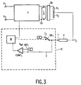
- the embodiment shown in Fig. 3 utilizes, as does the embodiment shown in Fig. 2, only one internal reference value.
- the electrical quantity G in this embodiment is the current through the input terminal T, whose first value is I1 and whose second value is I2.
- I2 is chosen to be equal to zero here.
- circuit portion A is replaced by circuit portion A' for generating a current with amplitude I1
- circuit portion E is formed by a conductive connection between input terminal T and an input of comparator Comp1.
- the construction of the embodiment shown in Fig. 3 corresponds to that of the embodiment shown in Fig. 2 in other respects, and corresponding components and circuit portions have been given the same reference symbols.
- a signal S which is a measure for the voltage across the discharge lamp La is present at terminal Ts both during the ignition phase and during stationary lamp operation.
- the circuit portion III periodically changes the state of switching element Sw1 from a first to a second state and vice versa.
- input terminal T is connected to the output of circuit portion A'.
- a current with amplitude 11 flows through the input terminal T.
- the current through the input terminal T is equal to zero in the second state.
- Comparator Comp1 compares the internal signal S int formed by the voltage at input terminal T with the internal reference signal generated by the circuit portion C in both states. If the internal reference signal is exceeded in either state, the means III are activated via the output of comparator Comp1 and the input of circuit portion III.
- the ratio of the resistance values of ohmic resistors R1 and R2 is chosen such that the signal S at terminal Ts reaches the value S1 when the voltage across the discharge lamp reaches its maximum admissible value. Given this ratio of the resistance values of ohmic resistors R1 and R2 , the signal at terminal Ts will reach the value S2 when the voltage across the discharge lamp La reaches its minimum admissible value.
- the internal reference value corresponds to the external reference value S1 in the first state of the integrated circuit and to the external reference value S2 in the second state of the integrated circuit, provided the value of ohmic resistor R is in accordance with the equation. It is thus possible also in this embodiment to adjust the reference values S1 and S2 independently of one another to desired levels through a suitable choice of the resistance values of R1 and R2.
Abstract
Description
- The invention relates to a circuit arrangement for operating a discharge lamp, provided with
- input terminals for coupling to a supply voltage source,
- means I coupled to the input terminals for generating a current through the discharge lamp from a supply voltage delivered by the supply voltage source,
- a control circuit for controlling the operational state of the means I, comprising
- means II for generating a signal S which is a measure for the value of an operating parameter,
- an integrated circuit provided with
- an input terminal T coupled to the means II,
- means C for generating a first internal reference signal,
- means E coupled to input terminal T for generating an internal signal Sint derived from signal S,
- comparator means Comp provided with an output, a first input coupled to the means C, and a second input coupled to the means E, and
- means III coupled to the output of the comparator means Comp for changing the operational state of the means I.
- Such a circuit arrangement is known from US 4,952,849. The signal S in the known circuit arrangement which is a measure for a value of an operating parameter is a signal which is a measure for the current through the discharge lamp (also referred to as lamp hereinafter). The control circuit achieves that the amplitude of the current through the lamp remains approximately constant. It is also possible to choose an alternative operating parameter such as, for example, the voltage across the lamp. If, for example, the discharge lamp fails to ignite after the circuit arrangement has been switched on, the voltage across the discharge lamp will rise to the point where the internal signal Sint exceeds the value of the first internal reference signal. This activates the means III. The means III effect a change in the operating state of the means I such that this causes the voltage across the discharge lamp to drop. It can be achieved thereby that the voltage across the discharge lamp is not maintained at a high value by the circuit arrangement for a long period if the discharge lamp should fail to ignite. It is desirable in many cases not only to provide measures which ensure that the value of an operating parameter does not exceed a maximum admissible value (for a long period), but also to ensure that the same operating parameter cannot assume an undesirably low value. If the operating parameter is the voltage across the discharge lamp, a (too) low value of this voltage may point to a (too) high value of the current through the discharge lamp or a defect in a capacitor connected parallel to the discharge lamp. It may also be desirable, for example, to limit the voltage across the discharge lamp to a first maximum admissible value during ignition and to a second maximum admissible value during stationary lamp operation, which latter value must not be exceeded for more than a predetermined time interval. A change in the operational state of the means I is indicated, for example switching-off of the means I, if a maximum or minimum admissible value is exceeded. It is possible to design the control circuit such that the means II are coupled to only one input terminal of the integrated circuit, and that one and the same signal Sint is compared with a first internal reference signal and with a second internal reference signal. Such a construction of the control circuit, however, renders it necessary to lay down the relationship between the two internal reference signals in the integrated circuit. The relationship between the two reference values, for example the relationship between the minimum admissible value and the maximum admissible value of the operating parameter, is then also laid down in such a construction of the control circuit. The minimum admissible value and the maximum admissible value of an operating parameter, such as the voltage across the discharge lamp, however, are generally speaking dependent on specific properties of the discharge lamp and of the construction of the circuit arrangement. It is desirable for this reason to have a possibility of setting these reference values independently of one another. This is possible through the use of two input terminals of the integrated circuit. These two input terminals are coupled to the means II in that case, and each of the input terminals is coupled to comparator means and means for generating a reference signal. Such a solution, however, requires a comparatively large number of input terminals, which renders the integrated circuit large and expensive. In addition, this solution often requires a comparatively large number of external components, so that the circuit arrangement becomes complicated and expensive.
- The invention has for its object to provide a circuit arrangement of the kind mentioned in the opening paragraph with which it is possible to adjust two reference values of the signal S independently of one another, while the means II are coupled to only one input terminal.
- According to the invention, a circuit arrangement of the kind mentioned in the opening paragraph is for this purpose characterized in that the means II are coupled to the input terminal T via an impedance P, and in that the integrated circuit is in addition provided with
- means D coupled to the comparator means Comp for generating a second internal reference signal,
- means IV for changing the amplitude of an electrical quantity G present at the input terminal T from a first to a second value, and for changing the operational state of the comparator means Comp from a first state to a second state, said comparator means Comp comparing the internal signal Sint with the first internal reference signal in the first state and comparing the internal signal Sint with the second internal reference signal in the second state.
- The comparator means Comp are in the first state when the amplitude of the electrical quantity G has the first value, in which case the internal signal Sint is compared with the first internal reference signal. This means that the signal S is compared with a first reference value derived from the first internal reference signal. If the amplitude of the electrical quantity G has the second value, the internal signal Sint is compared with the second internal reference signal. This means that the signal S is compared with a second reference value derived from the second internal reference signal. Although the first and the second internal reference signal have been laid down in the integrated circuit, it is possible to adjust the first and the second reference value independently of one another by means of the impedance value of impedance P and the dimensioning of the means II.
- The means III change the operational state of the means I whenever the signal S has passed one of these reference values.
- The electrical quantity G may be the voltage present at the input terminal T, in which case the means IV are provided with means for changing the amplitude of the voltage present at the input terminal from a first value V1 to a second value V2. Preferably, the second value V2 is chosen to be zero. The integrated circuit may be of a comparatively simple construction in that case.
- The electrical quantity G may alternatively be the current flowing through the input terminal. In that case the means IV are provided with means for changing the amplitude of the current flowing through the input terminal from a first value I1 to a second value I2. It is advantageous in this latter case for the means IV to comprise a first current source and a second current source, the first current source supplying a current whose amplitude is equal to the first value I1 and the second current source supplying a current whose amplitude is equal to the second value 12. Preferably, the second value I2 is chosen to be zero. The integrated circuit can be of a comparatively simple construction then.
- Preferably, the means IV are provided with means IVa for periodically changing the amplitude of the electrical quantity G from the first value to the second value and vice versa with a frequency f and for periodically changing the operational state of the comparator means Comp from the first state to the second state and vice versa. It is possible in that case to repeat the comparison of the signal S with the reference values continuously and thus to monitor the relevant operating parameter during a longer period. If the means I comprise at least a switching element and means IVb for rendering the switching element conducting and non-conducting during lamp operation, the frequency with which the switching element is rendered conducting and non-conducting is preferably chosen to be equal to the frequency f, and the changes in amplitude of the electrical quantity G and in the operational state of the comparator means Comp take place in synchronity with the cycle in which the switching element is rendered conducting and non-conducting:
- Good results were obtained with embodiments of the circuit arrangement according to the invention in which the impedance comprises an ohmic resistance.
- A comparatively simple construction of the integrated circuit is possible if the first internal reference signal is equal to the second internal reference signal, and the means D are formed by the means C.
- Embodiments of a circuit arrangement according to the invention will be explained in more detail with reference to a drawing, in which
- Figs. 1, 2 and 3 are diagrams of embodiments of a circuit arrangement according to the invention.
- In Fig. 1, K1 and K2 form input terminals for coupling to a supply voltage source. Circuit portion I in this embodiment forms means I coupled to the input terminals for generating a current through the discharge lamp from a supply voltage delivered by the supply voltage source. The current through the discharge lamp is a high-frequency alternating current in this embodiment. A discharge lamp La is connected to respective output terminals of the means I.
- Ohmic resistors R1 and R2 together with circuit portion IIa form means II in this embodiment for generating a signal S which is a measure for the value of an operating parameter. The operating parameter is the amplitude of the AC voltage present across the discharge lamp La during lamp operation in this embodiment. Circuit portion IIa may comprise, for example, means for generating a DC voltage signal which is a measure for the rms value of the voltage across the discharge lamp. Another possibility is that circuit portion . IIa comprises means for generating a DC voltage signal which is a measure for the sum of the amplitudes of the voltages across the discharge lamp in both directions. Ohmic resistor P in this embodiment forms an impedance P. The other circuit portions and components shown in Fig. 1 together form an integrated circuit IC. T is an input terminal of the integrated circuit IC which is coupled to the means II via ohmic resistor P. Circuit portion IVa together with switching element Sw1 and switching element Sw2 forms means IV and at the same time means for periodically changing the amplitude of an electrical quantity G present at the input terminal from a first to a second value and vice versa and for changing the operational state of the comparator means Comp from a first state to a second state, said comparator means Comp comparing an internal signal Sint with a first internal reference signal in the first state and comparing the internal signal Sint with a second internal reference signal in the second state.
The quantity G present at the input terminal in this embodiment is formed by the voltage applied to the input terminal, having a first value V1 and a second value V2. A, B, C and D are circuit portions for generating, in that order, a voltage whose amplitude is equal to the first value V1, a voltage whose amplitude is equal to the second value V2, a voltage which in this embodiment forms the first internal reference signal, and a voltage which in this embodiment forms the second reference signal. Furthermore, the integrated circuit IC comprises a circuit portion E, two comparators Comp1 and Comp2, and a circuit portion III which in this embodiment forms the means III for changing the operational state of the means I when the signal S has passed a reference value which is derived from the internal reference signal. The circuit portion E in this embodiment forms means E for generating the internal signal Sint which is derived from the signal S. The comparators Comp1 and Comp2 in this embodiment form the comparator means Comp. - Ends of the discharge lamp La are connected to respective inputs of circuit portion lla. A first output of circuit portion lla is connected to a second output by means of a series circuit of ohmic resistor R1 and ohmic resistor R2. A common junction point of ohmic resistor R1 and ohmic resistor R2 is connected to terminal Ts. Terminal Ts is connected to input terminal T via ohmic resistor P. Input terminal T is connected to a first main electrode of switching element Sw1. A second and a third main electrode of switching element Sw1 are connected to an output of circuit portion A and an output of circuit portion B, respectively. E is a circuit portion for generating a voltage which is proportional to the current through the input terminal T. An input of circuit portion E is for this purpose coupled to input terminal T. An output of circuit portion E is connected to a first main electrode of switching element Sw2. A second and a third main electrode of switching element Sw2 are connected to an input of comparator Comp1 and to an input of comparator Comp2, respectively. A further input of comparator Comp1 is connected to an output of circuit portion C, and a further input of comparator Comp2 is connected to an output of circuit portion D. Outputs of the circuit portion IVa are coupled to respective control electrodes of switching elements Sw1 and Sw2. This coupling is indicated with broken lines in Fig. 1. An output of comparator Comp1 is connected to an input of circuit portion III. An output of comparator Comp2 is connected to a further input of circuit portion III. An output of circuit portion III is connected to an input of circuit portion I.
- The operation of the circuit arrangement shown in Fig. 1 is as follows.
- When the input terminals K1 and K2 are connected to a supply voltage source, the means I generate a high-frequency alternating current through the discharge lamp from a supply voltage delivered by this supply voltage source during stationary lamp operation. Before the stationary lamp operation phase, the circuit portion I generates an ignition voltage across the discharge lamp La during the ignition phase. A signal S, which is generated by the means II and which is a measure for the amplitude of the voltage across the discharge lamp La, is present at terminal Ts both during the ignition phase and during stationary lamp operation. The circuit portion IVa periodically switches the integrated circuit from a first to a second state and vice versa by means of switching elements Sw1 and Sw2. In the first state, the input terminal T is connected to the output of circuit portion A, and the output of circuit portion E is connected to the further input of comparator Comp1. Voltage V1 is present at the input terminal T. In the second state, input terminal T is connected to the output of circuit portion B, and the output of circuit portion E is connected to the further input of comparator Comp2. Voltage V2 is present at the input terminal T. The outputs of comparators Comp1 and Comp2 are both low immediately after the circuit arrangement has been switched on. If the voltage present at the output of circuit portion E is higher than the first internal reference value in the first state, the output of comparator Comp1 will change from low to high, which activates the circuit portion III and changes the operational state of the circuit portion I. The following equation holds for the voltage S1 at terminal Ts if that current through input terminal T for which the voltage Sint at the output of circuit portion E is equal to the first internal reference value is equal to I1:

in which (R)P is the resistance value of ohmic resistor P.
This voltage S1 is the first reference value of the signal S. The signal S is accordingly compared with the first reference value S1 in the first state, S1 being dependent on the current I1, which in its turn is determined by the first internal reference value formed by the output voltage of circuit portion C via circuit portion E. The operational state of circuit portion I is changed if the signal S exceeds the first reference value S1. - The output of comparator Comp2 changes from low to high, whereby the circuit portion III is activated and the operational state of the circuit portion I is changed, if in the second state the voltage Sint present at the output of circuit portion E is lower than the second internal reference value. The following is true for the voltage S2 at terminal Ts if the current through input terminal T for which the voltage at the output of circuit portion E is equal to the second internal reference value is equal to I2:

This voltage S2 is the second reference value of the signal S. The signal S is accordingly compared with the second reference value S2 in the second state, S2 being determined by current I2 which in its turn is determined via circuit portion E by the second internal reference value formed by the output voltage of circuit portion D. The operational state of circuit portion I is changed if the signal S is lower than the second reference value S2. - The ratio I1/I2 = y is a fixed one because the circuit portions E, C and D form part of the integrated circuit IC. If the desired ratio of the first and the second reference signals S1/S2 is x, substitution of x and y in equation I and equation II gives:


- It is also true that:

- The ratio of the resistance values of ohmic resistors R1 and R2 is chosen such that the signal S at terminal Ts reaches the value S1 when the voltage across the discharge lamp reaches its maximum admissible value. Given this ratio of the resistance values of ohmic resistors R1 and R2, the signal at terminal Ts will reach the value S2 when the voltage across the discharge lamp La reaches its minimum admissible value. The internal reference values I1 and I2 correspond to the external reference values S1 and S2 given the value of ohmic resistor R in accordance with the equation. It is thus possible to adjust the reference values S1 and S2 mutually independently to desired levels through a suitable choice of the resistors R1, R2 and R.
- The embodiment shown in Fig. 1 can be substantially simplified. If the integrated circuit is so constructed that I1/I2 = y is equal to 1, the first internal reference value will be equal to the second internal reference value. Only one circuit portion for generating the internal reference value is required in such an embodiment of the integrated 4 circuit IC. Since the internal signal Sint is to be compared with only a single internal reference value, the comparator means Comp need comprise only one comparator, and the switching element Sw2 is also redundant. A further simplification may be obtained in that the amplitude of voltage V2 is chosen to be equal to zero. Circuit portion B may now be formed in that the relevant main electrode of the switching element Sw1 is connected to ground potential. The integrated circuit IC can be of a comparatively simple construction as a result of this. Circuit portion I of the embodiment shown in Fig. 1 comprises a bridge circuit which contains two switching elements which are rendered conducting and non-conducting alternately with a high frequency f for generating the high-frequency current through the discharge lamp. A further advantage over the embodiment shown in Fig. 1 may be realized in that the switching element Sw1 changes the value of the voltage at input terminal T with the same frequency f, in synchronity with the cycle in which the switching elements in the bridge circuit are rendered conducting and non-conducting. The process of rendering the switching elements of the bridge circuit conducting and non-conducting gives rise to interference signals which are also present at terminal Ts and which accordingly can influence the value of the signal S. The interference generated by this switching, however, cannot influence the result of the comparison between the internal signal Sint and the internal reference signal by the comparator means Comp if the switching of the switching elements in the bridge and in the integrated circuit is carried out in synchronity, and said comparison is carried out only in a time interval within which no switching takes place. Fig. 2 shows an embodiment of a circuit arrangement according to the invention in which the improvements mentioned in the present paragraph relative to the embodiment of Fig. 1 have been implemented. The control signal which controls both the switching elements of the bridge circuit and switching element Sw1 is generated by circuit portion III, which comprises the means III as well as the means IV in the embodiment shown in Fig. 2. An output of circuit portion III is for this purpose coupled to switching element Sw1. This coupling is indicated with a broken line in Fig. 2. The output of circuit portion III coupled to circuit portion I is coupled to control electrodes of the switching elements of the bridge circuit which forms part of circuit portion I. Compared with the embodiment shown in Fig. 1, circuit portion B, circuit portion D, comparator Comp2, and switching element Sw2 are absent here. In addition, only one input of circuit portion III is coupled to the comparator means Comp. The construction of the embodiment shown in Fig. 2 corresponds to that of the embodiment shown in Fig. 1 in other respects, and corresponding components and circuit portions have been given the same reference symbols.
- The operation of the circuit arrangement shown in Fig. 2 is as follows.
- When the input terminals K1 and K2 are connected to a supply voltage source, the means I generate a high-frequency alternating current through the discharge lamp from a supply voltage delivered by this supply voltage source during stationary lamp operation. Before the stationary lamp operation phase, the circuit portion I generates an ignition voltage across the discharge lamp La during the ignition phase. A signal S generated by the means II is present at terminal Ts both during the ignition phase and during stationary lamp operation, signal S being a measure for the amplitude of the voltage across the discharge lamp La. The circuit portion III periodically changes the state of switching element Sw1 from a first to a second state and vice versa. Input terminal T is connected to the output of circuit portion A in the first state. Voltage V1 is present at the input terminal T. Input terminal T is connected to ground potential in the second state. Comparator Comp1 compares the internal signal Sint generated by the circuit portion E with the internal reference signal generated by circuit portion C in both states. If the internal reference signal is exceeded in either state, the means III are activated via the output of comparator Comp1 and the input of circuit portion III. The means III change the operational state of the circuit portion I, for example by switching off circuit portion I.
The equations which are true for the embodiment shown in Fig. 2 are:


The ratio of the resistance values of ohmic resistors R1 and R2 is chosen such that the signal S at terminal Ts reaches the value S1 when the voltage across the discharge lamp reaches its maximum admissible value. Given this ratio of the resistance values of ohmic resistors R1 and R2, the signal at terminal Ts will reach the value S2 when the voltage across the discharge lamp La reaches its minimum admissible value. With the value of ohmic resistor R as given by the equation, the internal reference value will correspond to the external reference value S1 with the integrated circuit in the first state and to the external reference value S2 with the integrated circuit in the second state. It is thus possible also in this embodiment to adjust the reference values S1 and S2 independently of one another to desired levels through a suitable choice of the resistance values of R1 and R2. - The embodiment shown in Fig. 3 utilizes, as does the embodiment shown in Fig. 2, only one internal reference value. The electrical quantity G in this embodiment is the current through the input terminal T, whose first value is I1 and whose second value is I2. I2 is chosen to be equal to zero here. The differences with the embodiment shown in Fig. 2 are that circuit portion A is replaced by circuit portion A' for generating a current with amplitude I1, and that circuit portion E is formed by a conductive connection between input terminal T and an input of comparator Comp1. The construction of the embodiment shown in Fig. 3 corresponds to that of the embodiment shown in Fig. 2 in other respects, and corresponding components and circuit portions have been given the same reference symbols.
- The operation of the embodiment shown in Fig. 3 is as follows.
- A signal S which is a measure for the voltage across the discharge lamp La is present at terminal Ts both during the ignition phase and during stationary lamp operation. The circuit portion III periodically changes the state of switching element Sw1 from a first to a second state and vice versa. In the first state, input terminal T is connected to the output of circuit portion A'. A current with amplitude 11 flows through the input terminal T. The current through the input terminal T is equal to zero in the second state. Comparator Comp1 compares the internal signal Sint formed by the voltage at input terminal T with the internal reference signal generated by the circuit portion C in both states. If the internal reference signal is exceeded in either state, the means III are activated via the output of comparator Comp1 and the input of circuit portion III. The means III change the operational state of the circuit portion I, for example by switching off the circuit portion I. If the voltage at input terminal T is equal to the internal reference value V1 at the output of circuit portion C, it will be true for the embodiment shown in Fig. 3 that the voltage S1 at terminal Ts is:

in which (R)P is the resistance value of ohmic resistor P. This voltage S1 is the first reference voltage of the signal S. It is true in the second state that, if the voltage at input terminal T is equal to the internal reference value V1, the voltage S2 at terminal Ts is:
- Since the amplitude of I2 was chosen to be zero, these equations may alternatively be written as:


- The ratio of the resistance values of ohmic resistors R1 and R2 is chosen such that the signal S at terminal Ts reaches the value S1 when the voltage across the discharge lamp reaches its maximum admissible value. Given this ratio of the resistance values of ohmic resistors R1 and R2, the signal at terminal Ts will reach the value S2 when the voltage across the discharge lamp La reaches its minimum admissible value. The internal reference value corresponds to the external reference value S1 in the first state of the integrated circuit and to the external reference value S2 in the second state of the integrated circuit, provided the value of ohmic resistor R is in accordance with the equation. It is thus possible also in this embodiment to adjust the reference values S1 and S2 independently of one another to desired levels through a suitable choice of the resistance values of R1 and R2.
Claims (10)
- A circuit arrangement for operating a discharge lamp (LA), provided with- input terminals (K1, K2) for coupling to a supply voltage source,- means I coupled to the input terminals for generating a current through the discharge lamp from a supply voltage delivered by the supply voltage source,- a control circuit for controlling the operational state of the means I, comprising- means II for generating a signal S which is a measure for the value of an operating parameter,- an integrated circuit provided with- an input terminal T coupled to the means II;- means C for generating a first internal reference signal,- means D for generating a second internal reference signal,- means E coupled to input terminal T for generating an internal signal Sint derived from signal S,- a first comparator means (Comp1) provided with an output, a first input coupled to the means C, and a second input coupled to the means- E,- second comparator (Comp 2) provided with an output, a first input coupled to the means E, and a second input coupled to the means D,- means III coupled to the output of the first and second comparator means for changing the operational state of the means I,- the means II are coupled to the input terminal T via an impedance P,- means IV for changing the amplitude of an electrical quantity G present at the input terminal T from a first to a second value, and for thereby changing the value of Sint from a first to a second value and for changing the operational state of the first and second comparator means from a first state to a second state, characterized in that said first comparator means (Comp1) exclusively compare the first value of the internal signal Sint with the first internal reference signal in the first state and said second comparator means (Comp2) exclusively compare the second value of the internal signal Sint with the second internal reference signal in the second state.
- A circuit arrangement as claimed in Claim 1, wherein the electrical quantity G is the voltage applied to the input terminal, and means IV are provided with means (IVA, SW1, A, B) for changing the amplitude of the voltage applied to the input terminal from a first value V1 to a second value V2.
- A circuit arrangement as claimed in Claim 2, wherein the second value V2 is equal to zero.
- A circuit arrangement as claimed in Claim 1, wherein the electrical quantity G is the current flowing through the input terminal, and the means IV are provided with means (IVA, SW1, A, B) for changing the amplitude of the current flowing through the input terminal from a first value I1 to a second value I2.
- A circuit arrangement as claimed in Claim 4, wherein the second value I2 is equal to zero.
- A circuit arrangement as claimed in any one or several of the preceding Claims, wherein the means IV are provided with means (IVA) for periodically changing the amplitude of the electrical quantity G from the first to the second value and vice versa with a frequency f, and for periodically changing the operational state of the comparator means Comp from the first state to the second state and vice versa.
- A circuit arrangement as claimed in Claim 6, wherein the means I comprise at least a switching element and means for rendering said switching element conducting and non-conducting with the frequency f during lamp operation in synchronity with the change in amplitude of the electrical quantity G and the change in the operational state of the comparator means Comp.
- A circuit arrangement as claimed in any one or several of the preceding Claims, wherein the impedance P comprises an ohmic resistor.
- A circuit arrangement as claimed in any one or several of the preceding Claims, wherein the first internal reference signal is equal to the second internal reference signal, and the means D are formed by the means C.
- A circuit arrangement as claimed in any one or several of the preceding claims, wherein comparator Comp2 is formed by comparator Comp1.
Priority Applications (1)
| Application Number | Priority Date | Filing Date | Title |
|---|---|---|---|
| EP97927320A EP0860098B1 (en) | 1996-09-11 | 1997-07-04 | Circuit arrangement |
Applications Claiming Priority (4)
| Application Number | Priority Date | Filing Date | Title |
|---|---|---|---|
| EP96202533 | 1996-09-11 | ||
| EP96202533 | 1996-09-11 | ||
| EP97927320A EP0860098B1 (en) | 1996-09-11 | 1997-07-04 | Circuit arrangement |
| PCT/IB1997/000828 WO1998011763A1 (en) | 1996-09-11 | 1997-07-04 | Circuit arrangement |
Publications (2)
| Publication Number | Publication Date |
|---|---|
| EP0860098A1 EP0860098A1 (en) | 1998-08-26 |
| EP0860098B1 true EP0860098B1 (en) | 2006-07-05 |
Family
ID=8224372
Family Applications (1)
| Application Number | Title | Priority Date | Filing Date |
|---|---|---|---|
| EP97927320A Expired - Lifetime EP0860098B1 (en) | 1996-09-11 | 1997-07-04 | Circuit arrangement |
Country Status (6)
| Country | Link |
|---|---|
| US (1) | US5959411A (en) |
| EP (1) | EP0860098B1 (en) |
| JP (1) | JP2000500279A (en) |
| CN (1) | CN1150806C (en) |
| DE (1) | DE69736273T2 (en) |
| WO (1) | WO1998011763A1 (en) |
Families Citing this family (4)
| Publication number | Priority date | Publication date | Assignee | Title |
|---|---|---|---|---|
| DE10021537A1 (en) * | 2000-05-03 | 2001-11-08 | Philips Corp Intellectual Pty | Method and device for operating a gas discharge lamp |
| US20050073784A1 (en) * | 2003-10-02 | 2005-04-07 | Dell Products L.P. | Modular DC-DC standby voltage converter having programmable sequencing |
| NZ591896A (en) | 2008-08-29 | 2013-03-28 | Treventis Corp | Compositions and methods of treating amyloid disease |
| US7982452B2 (en) | 2009-07-30 | 2011-07-19 | Infineon Technologies Austria Ag | Detection of a load state of a half-bridge |
Family Cites Families (7)
| Publication number | Priority date | Publication date | Assignee | Title |
|---|---|---|---|---|
| DE3149526A1 (en) * | 1981-12-14 | 1983-06-23 | Philips Patentverwaltung | CIRCUIT ARRANGEMENT FOR OPERATING HIGH PRESSURE GAS DISCHARGE LAMPS |
| US4870327A (en) * | 1987-07-27 | 1989-09-26 | Avtech Corporation | High frequency, electronic fluorescent lamp ballast |
| US4952849A (en) * | 1988-07-15 | 1990-08-28 | North American Philips Corporation | Fluorescent lamp controllers |
| US5198726A (en) * | 1990-10-25 | 1993-03-30 | U.S. Philips Corporation | Electronic ballast circuit with lamp dimming control |
| DE4102069A1 (en) * | 1991-01-24 | 1992-07-30 | Patent Treuhand Ges Fuer Elektrische Gluehlampen Mbh | CIRCUIT ARRANGEMENT FOR OPERATING A DISCHARGE LAMP |
| DE69220456T2 (en) * | 1991-11-13 | 1998-01-02 | Philips Electronics Nv | Circuit arrangement |
| TW339496B (en) * | 1994-06-22 | 1998-09-01 | Philips Electronics Nv | Method and circuit arrangement for operating a high-pressure discharge lamp |
-
1997
- 1997-07-04 EP EP97927320A patent/EP0860098B1/en not_active Expired - Lifetime
- 1997-07-04 DE DE69736273T patent/DE69736273T2/en not_active Expired - Fee Related
- 1997-07-04 WO PCT/IB1997/000828 patent/WO1998011763A1/en active IP Right Grant
- 1997-07-04 JP JP10513420A patent/JP2000500279A/en not_active Ceased
- 1997-07-04 CN CNB971915679A patent/CN1150806C/en not_active Expired - Fee Related
- 1997-07-11 US US08/891,604 patent/US5959411A/en not_active Expired - Fee Related
Also Published As
| Publication number | Publication date |
|---|---|
| US5959411A (en) | 1999-09-28 |
| DE69736273T2 (en) | 2007-07-05 |
| DE69736273D1 (en) | 2006-08-17 |
| EP0860098A1 (en) | 1998-08-26 |
| JP2000500279A (en) | 2000-01-11 |
| WO1998011763A1 (en) | 1998-03-19 |
| CN1150806C (en) | 2004-05-19 |
| CN1207236A (en) | 1999-02-03 |
Similar Documents
| Publication | Publication Date | Title |
|---|---|---|
| CN1052372C (en) | Discharge lamp lighting device | |
| JPH04264397A (en) | Electric-discharge-lamp lighting circuit | |
| US5172033A (en) | Discharge lamp operating inverter circuit with electric dimmer utilizing frequency control of the inverter | |
| JP3236018B2 (en) | Circuit device for discharge lamp lighting | |
| JP4405396B2 (en) | Circuit for operating a discharge lamp | |
| EP0860098B1 (en) | Circuit arrangement | |
| US5670849A (en) | Circuit arrangement | |
| JPH0778696A (en) | Discharge lamp lighting circuit | |
| EP0788680B1 (en) | Electronic lamp ballast comprising a bridge circuit and an integrated circuit arrangement provided with a voltage-current converter for controlling the bridge circuit | |
| EP0838128B1 (en) | Circuit arrangement | |
| KR100291608B1 (en) | Circuit device | |
| WO2002075908A1 (en) | Dc-dc converter. | |
| JP4537378B2 (en) | Lamp lighting circuit layout | |
| JPH06233523A (en) | Frequency-modulation type switching power supply circuit | |
| US7525260B2 (en) | Discharge lamp lighting apparatus | |
| EP1342393B1 (en) | Digital ballast | |
| JPS61260598A (en) | Gas discharge lamp lighting circuit array | |
| WO1998010623A1 (en) | Circuit arrangement | |
| US20030232602A1 (en) | Apparatus for switching matching circuit in mobile communication terminal | |
| SU1525804A1 (en) | Phase inditcator | |
| KR100919718B1 (en) | Burst dimming circuit and method thereof | |
| SU1283909A2 (en) | A.c.voltage-to-a.c.voltage converter for testing installations | |
| AU2010330232A1 (en) | Circuit assembly for operating at least one discharge lamp | |
| JPH03215827A (en) | Dimming device | |
| JPS6069569A (en) | Conduction checker |
Legal Events
| Date | Code | Title | Description |
|---|---|---|---|
| PUAI | Public reference made under article 153(3) epc to a published international application that has entered the european phase |
Free format text: ORIGINAL CODE: 0009012 |
|
| AK | Designated contracting states |
Kind code of ref document: A1 Designated state(s): DE FR GB |
|
| 17P | Request for examination filed |
Effective date: 19980921 |
|
| 17Q | First examination report despatched |
Effective date: 20020108 |
|
| APBN | Date of receipt of notice of appeal recorded |
Free format text: ORIGINAL CODE: EPIDOSNNOA2E |
|
| APBR | Date of receipt of statement of grounds of appeal recorded |
Free format text: ORIGINAL CODE: EPIDOSNNOA3E |
|
| APBV | Interlocutory revision of appeal recorded |
Free format text: ORIGINAL CODE: EPIDOSNIRAPE |
|
| GRAP | Despatch of communication of intention to grant a patent |
Free format text: ORIGINAL CODE: EPIDOSNIGR1 |
|
| GRAS | Grant fee paid |
Free format text: ORIGINAL CODE: EPIDOSNIGR3 |
|
| APBD | Information on interlocutory revision deleted |
Free format text: ORIGINAL CODE: EPIDOSDIRAPE |
|
| APBV | Interlocutory revision of appeal recorded |
Free format text: ORIGINAL CODE: EPIDOSNIRAPE |
|
| GRAA | (expected) grant |
Free format text: ORIGINAL CODE: 0009210 |
|
| AK | Designated contracting states |
Kind code of ref document: B1 Designated state(s): DE FR GB |
|
| REG | Reference to a national code |
Ref country code: GB Ref legal event code: FG4D |
|
| RIC1 | Information provided on ipc code assigned before grant |
Ipc: H05B 41/292 20060101AFI20060526BHEP |
|
| REF | Corresponds to: |
Ref document number: 69736273 Country of ref document: DE Date of ref document: 20060817 Kind code of ref document: P |
|
| EN | Fr: translation not filed | ||
| PLBE | No opposition filed within time limit |
Free format text: ORIGINAL CODE: 0009261 |
|
| STAA | Information on the status of an ep patent application or granted ep patent |
Free format text: STATUS: NO OPPOSITION FILED WITHIN TIME LIMIT |
|
| 26N | No opposition filed |
Effective date: 20070410 |
|
| PGFP | Annual fee paid to national office [announced via postgrant information from national office to epo] |
Ref country code: DE Payment date: 20070919 Year of fee payment: 11 |
|
| GBPC | Gb: european patent ceased through non-payment of renewal fee |
Effective date: 20070704 |
|
| PG25 | Lapsed in a contracting state [announced via postgrant information from national office to epo] |
Ref country code: FR Free format text: LAPSE BECAUSE OF FAILURE TO SUBMIT A TRANSLATION OF THE DESCRIPTION OR TO PAY THE FEE WITHIN THE PRESCRIBED TIME-LIMIT Effective date: 20070511 |
|
| PG25 | Lapsed in a contracting state [announced via postgrant information from national office to epo] |
Ref country code: GB Free format text: LAPSE BECAUSE OF NON-PAYMENT OF DUE FEES Effective date: 20070704 |
|
| PG25 | Lapsed in a contracting state [announced via postgrant information from national office to epo] |
Ref country code: FR Free format text: LAPSE BECAUSE OF FAILURE TO SUBMIT A TRANSLATION OF THE DESCRIPTION OR TO PAY THE FEE WITHIN THE PRESCRIBED TIME-LIMIT Effective date: 20060705 |
|
| PG25 | Lapsed in a contracting state [announced via postgrant information from national office to epo] |
Ref country code: DE Free format text: LAPSE BECAUSE OF NON-PAYMENT OF DUE FEES Effective date: 20090203 |