EP0853336B1 - Method forming preferred orientation-controlled platinum films using nitrogen - Google Patents
Method forming preferred orientation-controlled platinum films using nitrogen Download PDFInfo
- Publication number
- EP0853336B1 EP0853336B1 EP98400019A EP98400019A EP0853336B1 EP 0853336 B1 EP0853336 B1 EP 0853336B1 EP 98400019 A EP98400019 A EP 98400019A EP 98400019 A EP98400019 A EP 98400019A EP 0853336 B1 EP0853336 B1 EP 0853336B1
- Authority
- EP
- European Patent Office
- Prior art keywords
- nitride
- platinum film
- film
- platinum
- substrate
- Prior art date
- Legal status (The legal status is an assumption and is not a legal conclusion. Google has not performed a legal analysis and makes no representation as to the accuracy of the status listed.)
- Expired - Lifetime
Links
Images






Classifications
-
- H—ELECTRICITY
- H10—SEMICONDUCTOR DEVICES; ELECTRIC SOLID-STATE DEVICES NOT OTHERWISE PROVIDED FOR
- H10D—INORGANIC ELECTRIC SEMICONDUCTOR DEVICES
- H10D1/00—Resistors, capacitors or inductors
- H10D1/60—Capacitors
- H10D1/68—Capacitors having no potential barriers
- H10D1/692—Electrodes
- H10D1/694—Electrodes comprising noble metals or noble metal oxides
-
- H—ELECTRICITY
- H10—SEMICONDUCTOR DEVICES; ELECTRIC SOLID-STATE DEVICES NOT OTHERWISE PROVIDED FOR
- H10P—GENERIC PROCESSES OR APPARATUS FOR THE MANUFACTURE OR TREATMENT OF DEVICES COVERED BY CLASS H10
- H10P14/00—Formation of materials, e.g. in the shape of layers or pillars
- H10P14/40—Formation of materials, e.g. in the shape of layers or pillars of conductive or resistive materials
- H10P14/412—Deposition of metallic or metal-silicide materials
-
- C—CHEMISTRY; METALLURGY
- C23—COATING METALLIC MATERIAL; COATING MATERIAL WITH METALLIC MATERIAL; CHEMICAL SURFACE TREATMENT; DIFFUSION TREATMENT OF METALLIC MATERIAL; COATING BY VACUUM EVAPORATION, BY SPUTTERING, BY ION IMPLANTATION OR BY CHEMICAL VAPOUR DEPOSITION, IN GENERAL; INHIBITING CORROSION OF METALLIC MATERIAL OR INCRUSTATION IN GENERAL
- C23C—COATING METALLIC MATERIAL; COATING MATERIAL WITH METALLIC MATERIAL; SURFACE TREATMENT OF METALLIC MATERIAL BY DIFFUSION INTO THE SURFACE, BY CHEMICAL CONVERSION OR SUBSTITUTION; COATING BY VACUUM EVAPORATION, BY SPUTTERING, BY ION IMPLANTATION OR BY CHEMICAL VAPOUR DEPOSITION, IN GENERAL
- C23C14/00—Coating by vacuum evaporation, by sputtering or by ion implantation of the coating forming material
- C23C14/06—Coating by vacuum evaporation, by sputtering or by ion implantation of the coating forming material characterised by the coating material
- C23C14/14—Metallic material, boron or silicon
- C23C14/16—Metallic material, boron or silicon on metallic substrates or on substrates of boron or silicon
- C23C14/165—Metallic material, boron or silicon on metallic substrates or on substrates of boron or silicon by cathodic sputtering
-
- C—CHEMISTRY; METALLURGY
- C23—COATING METALLIC MATERIAL; COATING MATERIAL WITH METALLIC MATERIAL; CHEMICAL SURFACE TREATMENT; DIFFUSION TREATMENT OF METALLIC MATERIAL; COATING BY VACUUM EVAPORATION, BY SPUTTERING, BY ION IMPLANTATION OR BY CHEMICAL VAPOUR DEPOSITION, IN GENERAL; INHIBITING CORROSION OF METALLIC MATERIAL OR INCRUSTATION IN GENERAL
- C23C—COATING METALLIC MATERIAL; COATING MATERIAL WITH METALLIC MATERIAL; SURFACE TREATMENT OF METALLIC MATERIAL BY DIFFUSION INTO THE SURFACE, BY CHEMICAL CONVERSION OR SUBSTITUTION; COATING BY VACUUM EVAPORATION, BY SPUTTERING, BY ION IMPLANTATION OR BY CHEMICAL VAPOUR DEPOSITION, IN GENERAL
- C23C14/00—Coating by vacuum evaporation, by sputtering or by ion implantation of the coating forming material
- C23C14/58—After-treatment
- C23C14/5806—Thermal treatment
-
- C—CHEMISTRY; METALLURGY
- C23—COATING METALLIC MATERIAL; COATING MATERIAL WITH METALLIC MATERIAL; CHEMICAL SURFACE TREATMENT; DIFFUSION TREATMENT OF METALLIC MATERIAL; COATING BY VACUUM EVAPORATION, BY SPUTTERING, BY ION IMPLANTATION OR BY CHEMICAL VAPOUR DEPOSITION, IN GENERAL; INHIBITING CORROSION OF METALLIC MATERIAL OR INCRUSTATION IN GENERAL
- C23C—COATING METALLIC MATERIAL; COATING MATERIAL WITH METALLIC MATERIAL; SURFACE TREATMENT OF METALLIC MATERIAL BY DIFFUSION INTO THE SURFACE, BY CHEMICAL CONVERSION OR SUBSTITUTION; COATING BY VACUUM EVAPORATION, BY SPUTTERING, BY ION IMPLANTATION OR BY CHEMICAL VAPOUR DEPOSITION, IN GENERAL
- C23C16/00—Chemical coating by decomposition of gaseous compounds, without leaving reaction products of surface material in the coating, i.e. chemical vapour deposition [CVD] processes
- C23C16/06—Chemical coating by decomposition of gaseous compounds, without leaving reaction products of surface material in the coating, i.e. chemical vapour deposition [CVD] processes characterised by the deposition of metallic material
-
- H—ELECTRICITY
- H10—SEMICONDUCTOR DEVICES; ELECTRIC SOLID-STATE DEVICES NOT OTHERWISE PROVIDED FOR
- H10D—INORGANIC ELECTRIC SEMICONDUCTOR DEVICES
- H10D1/00—Resistors, capacitors or inductors
- H10D1/60—Capacitors
- H10D1/68—Capacitors having no potential barriers
- H10D1/692—Electrodes
- H10D1/696—Electrodes comprising multiple layers, e.g. comprising a barrier layer and a metal layer
Definitions
- the present invention relates to a technique for depositing a platinum film, which may be used as a bottom electrode for capacitors of dynamic random access memory (DRAM) cells or of non-volatile memory cells and film sensors. More particularly, the invention relates to a technique for controlling the preferred orientation of the platinum films by depositing the platinum under an atmosphere containing nitrogen as well as an inert gas and then annealing to remove the nitrogen which was introduced during the deposition of the platinum. The present invention also relates to a method of manufacturing semiconductor devices or sensor devices comprising such platinum thin films.
- DRAM dynamic random access memory
- High-dielectric/ferroelectric materials are used for not only DRAM cells but also other electronic devices such as non-volatile ferroelectric memory devices, ferroelectric sensors or actuator devices, etc. Platinum is most favored, in particular, as a bottom electrode of such high-dielectric/ferroelectric devices.
- the favored high-dielectric and ferroelectric materials are oxides having perovskite structure, bismuth-layered perovskite structure and tungsten-bronze type structure along with ReMnO 3 (Re: rare earth element) and BaMF 4 (M: Mn, Co, Ni, Mg, Zn).
- a platinum thin film which is deposited on an insulating oxide layer by the conventional method, generally has a preferred (111) orientation. This is due to the fact that the plane with the minimum surface energy in metals with face centered cubic (FCC) structure is (111) and, considering only the surface energy at the depositing, the film is most stable if oriented toward (111).
- FCC face centered cubic
- US-A-5 440 173 relates to a high-temperature electrical contact for making contact to ceramic materials and to improved circuit element using the same ; said contact comprises a barrier layer of a titanium compound and a layer of platinum bonded to said barrier layer.
- Electrodes for ferroelectric thin films said electrodes being made of platinum and ruthenium oxide deposited by ion beam sputtering.
- the present invention provides a method of forming an orientation-controlled platinum film and a platinum film formed thereby, according to specific embodiments.
- the present invention also provides a method of manufacturing an electronic device comprising an orientation-controlled platinum film and an electronic device manufactured thereby.
- the present invention provides a method of freely controlling a preferred orientation of a platinum film by depositing a platinum film under an atmosphere containing nitrogen, and then annealing so that the preferred orientation of the platinum film becomes (111), (200) and/or (220).
- the present invention provides a method of forming a platinum film on a substrate comprising the steps of depositing a platinum film on the substrate under an atmosphere containing nitrogen together with an inert gas to deposit a platinum film containing a nitrogen component; and annealing the platinum film containing the nitrogen component to substantially remove the nitrogen component from the platinum film, whereby orientation of the platinum film can be controlled by changing at least one of the following parameters: the partial pressure ratio of the nitrogen to the entire total depositing atmosphere gas, the temperature of the substrate during the deposition step and the annealing conditions.
- the platinum film can be formed through two or more deposition steps, according to specific embodiments.
- the platinum film may be deposited by employing any one of the following methods: the direct current or radio frequency (DC/RF) magnetron sputtering, DC/RF sputtering, metal organic chemical vapor deposition, partially ionized beam deposition, vacuum evaporation, laser ablation.
- DC/RF direct current or radio frequency
- the method forming a platinum film described above can be applied to a process for manufacturing an electronic device by forming a high-dielectric or ferroelectric oxide film on the platinum film.
- the platinum film functions as a bottom electrode.
- a functional intermediate film such as an insulation layer, a conductive plug, an adhesion layer, or a diffusion barrier layer
- the present invention provides an electronic device with preferable characteristics which are required for DRAM or non-volatile memory devices.
- the present invention provides a method of manufacturing an orientation-controlled platinum film.
- Various specific embodiments of the present invention provide methods of freely controlling a preferred orientation of a platinum film by depositing a platinum film under an atmosphere containing nitrogen, and then annealing so that the orientation of the platinum film becomes (111), (200) and/or (220).
- the present invention provides for a preferred orientation-controlled platinum film that is formed over a substrate.
- the present invention deposits a platinum film on a substrate under an atmosphere containing nitrogen together with an inert gas to deposit a platinum film containing nitrogen; and anneals the platinum film containing nitrogen components to remove nitrogen components from the platinum film, whereby orientation of the platinum film can be controlled by changing at least one of the following parameters: the partial pressure ratio of the nitrogen to the entire total depositing atmosphere gas, the temperature of the substrate and the annealing conditions.
- An inert gas can be selected from Ar, Ne, Kr or Xe, in accordance with specific embodiments.
- the present invention can be applied to a process manufacturing an electronic device.
- a ferroelectric film may be formed on the platinum film, with the platinum film functioning, for example, as a bottom electrode.
- a functional intermediate film such as an insulation layer, a conductive plug, an adhesion layer, or a diffusion barrier layer
- Various materials which may be used for the different films are discussed in detail below and have general applicability to the following description of the specific embodiments.
- the material of the substrate may be selected from one of the following groups: single component semiconductor materials, e.g., silicon (Si), germanium (Ge) and diamond (C); compound semiconductor materials, e.g., GaAs, InP, SiGe and SiC; ceramic single crystals, e.g., SrTiO 3 , LaAlO 3 , Al 2 O 3 , KBr, NaCl, MgO, ZrO 2 , Si 3 N 4 , TiO 2 , Ta 2 O 5 , AlN or ceramic poly-crystals thereof; metals, e.g., Au, Ag, Al, Ir, Pt, Cu, Pd, Ru, W; and amorphous/glassy materials, e.g., BSG, PSG, BPSG, Si.
- single component semiconductor materials e.g., silicon (Si), germanium (Ge) and diamond (C)
- compound semiconductor materials e.g., GaAs, InP, SiGe and Si
- a functional intermediate film such as an insulating layer, a conductive plug layer, a diffusion barrier layer, or an adhesive or glue layer can be interposed between the platinum film and the substrate.
- the materials used for a functional intermediate film functioning as an insulating layer include SiO 2 , Si 3 N 4 , BPSG, MgO, CaO, CaF 2 , Al 2 O 3 or B 2 O 3 .
- the materials used for a functional intermediate film functioning as a conductive plug layer include TiN, zirconium nitride, titanium silicide, tantalum silicide, tungsten silicide, molybdenum silicide, nickel silicide, cobalt silicide, tantalum carbide, tantalum boride, polysilicon, germanium, W, Ta, Ti, Mo, TiW, boron carbide, Cu, and the like.
- the material used for a functional intermediate film which functions as a diffusion barrier layer can be selected from any one of the following groups: ternary component amorphous materials (Ti-Si-N, Ta-B-N, Ti-B-N), conductive nitride (titanium aluminum nitride, Zr nitride, Hf nitride, Y nitride, Se nitride, La nitride, rare earth nitride, N deficient Al nitride, doped Al nitride, Mg nitride, Ca nitride, Sr nitride, Ba nitride, TiN, GaN, Ni nitride, Ta nitride, Co nitride, W nitride), and the like.
- ternary component amorphous materials Ti-Si-N, Ta-B-N, Ti-B-N
- conductive nitride titanium aluminum nitrid
- the materials used for a functional intermediate film used for an adhesion or glue layer include TiN, W, Ta, Ti, Sn, Ru, In, Ir, Os, Rh, and silicide compound (Ni silicide, Co silicide, W silicide).
- the platinum film may be deposited by employing any one of the following methods: DC/RF magnetron sputtering, DC/RF sputtering, metal organic chemical vapor deposition, partially ionized beam deposition, vacuum evaporation, laser ablation.
- a method manufacturing an electronic device comprising a platinum film according to the present invention includes a step of forming a high-dielectric/ferroelectric film on top surface of a platinum film after depositing the platinum film.
- material used for the high-dielectric film or the ferroelectric film may be selected from any one of the following groups: a perovskite structure oxide, such as BT(BaTiO 3 ), BST(Ba 1-x Sr x TiO 3 ), ST(SrTiO 3 ), PT(PbTiO 3 ), PZT(Pb(Zr, Ti)O 3 ), PLT(Pb 1-x La x TiO 3 ), PLZT ((Pb 1-x La x ) (Zr y Ti z ) 1-x/4 O 3 ), PMN(PbMg 1/3 Nb 2/3 O 3 ), LiTaO 3 , KNbO 3 , K(Ta, Nb)O 3 , CaTiO 3 , S
- Figs. 1a to 1c are schematic cross-sectional views illustrating the steps of manufacturing an electronic device comprising a platinum film deposited according to one aspect of the present invention.
- a platinum film 104 is deposited on top surface of the substrate 100.
- the depositing atmosphere contains an inert gas (Ar, Ne, Xe, Kr, etc.) and nitrogen component, and under the temperature range between room temperature and 500°C. Accordingly, a nitrogen component is contained in the platinum film 104.
- the platinum film 104 formed on the substrate 100 is annealed under the temperature range between 400°C and 1,000°C to remove the nitrogen component from the platinum film 104. This process converts the platinum film 104 into the platinum film 108 which is substantially free from nitrogen components.
- the platinum film 108 has a high- dielectric/ferroelectric oxide film 112 thereon, as shown Fig.
- top electrode comprising the material identical with that of the bottom electrode, i.e., platinum or other conductive material.
- preferred orientation of the platinum film formed according to the above method can be controlled by at least any one of the following parameters: the partial pressure ratio of the nitrogen component to the entire gas of the platinum film deposition atmosphere, the temperature of the substrate during the deposition step or annealing conditions.
- the partial pressure ratio of the nitrogen component to the entire gas of the platinum film deposition atmosphere the temperature of the substrate during the deposition step or annealing conditions.
- Fig. 2 is a block diagram illustrating a modification to the method of Figs. 1a to 1c.
- an insulating layer 116 such as SiO 2 or Si 3 N 4 is formed between the substrate 100 and the platinum film 108 to be formed on top surface of the substrate 100.
- the platinum film 108 formed on the insulating layer 116 is deposited under an atmosphere containing a nitrogen component together with an inert gas and then annealed as shown in Fig. 1a.
- orientation of the platinum film can be controlled by changing at least one of the following parameters: the partial pressure ratio of the nitrogen component to the entire gas of the deposition atmosphere, the temperature of the substrate during the deposition step or annealing conditions.
- a platinum film can be deposited in two or more separate steps as shown in Figs. 3a to 3d which show the steps manufacturing an electronic device comprising a platinum film deposited according to another aspect of the present invention.
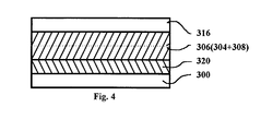
- a first thickness part 304 of the platinum film is deposited on the top surface of a substrate 300 under an inert gas atmosphere.
- a second thickness part 308 of the platinum film is deposited on the top surface of the first thickness part 304 under atmosphere containing nitrogen together with an inert gas as shown in Fig. 3b.
- Fig. 3c shows an annealing process to remove the gases incorporated during sputtering of the second thickness part 308. This process converts the platinum films 304 and 308 to the platinum film 306 which is substantially free of nitrogen components.
- Fig. 3a shows an annealing process to remove the gases incorporated during sputtering of the second thickness part 308. This process converts the platinum films 304 and 308 to the platinum film 306 which is substantially free of nitrogen components.
- an electronic device such as a capacitor is produced by forming a high-dielectric/ferroelectric oxide film 316 on the top surface of the annealed platinum film 306(304+308) and forming a top electrode (not shown in Fig. 3d) made from the same material as that of the bottom electrode or other conductive material.
- Fig. 4 is a block diagram illustrating a modification to the method illustrated in Figs. 3a to 3d, in which an insulating layer 320 is deposited for insulation between the substrate 300 and the platinum film 306.
- Figs. 3a to 3d and 4 illustrate methods depositing a platinum film in only two steps.
- the platinum film can also be deposited in three or more steps, according to other specific embodiments.
- inert gas of argon alone is employed in the first step to form a platinum film of the first deposited thickness.
- Argon gas mixed with a nitrogen component is employed in the second step to deposit a platinum film of a second deposited thickness.
- a platinum film of a third deposited thickness can be deposited in the remaining steps by employing inert gas or a mixture of inert gas with a nitrogen component.
- Fig. 5a represents a schematic diagram of an exemplary integrated circuit device, such as a DRAM cell with high-dielectric capacitors, which may be fabricated in accordance with the present invention.
- a transistor having a gate electrode 402 and source/drain regions 404.
- Gate electrode 402 which may be formed with doped or undoped polysilicon, is capped with a sidewall oxide layer 406, and field oxide 408 provides isolation.
- a high-dielectric capacitor is also formed in the DRAM cell region.
- the capacitor includes an upper capacitor cell plate 410, a bottom capacitor storage node 412, and a high dielectric constant material 414 formed between plate 410 and node 412.
- the capacitor is isolated from the transistor by an insulating layer 418, except through vias through layer 418 which are filled with a polysilicon plug layer 420.
- Insulating layer 418 may be made of SiO 2 , BPSG, etc.
- a diffusion barrier layer 416 is formed between bottom capacitor storage node 412 and polysilicon plug 420.
- the present invention may be used to deposit orientation-controlled platinum for use as bottom capacitor storage node 412 and/or upper capacitor cell plate 410.
- Fig. 5b represents a schematic diagram of an exemplary integrated circuit device, such as a non-volatile ferroelectric memory device, which may also be fabricated in accordance with the present invention.
- a non-volatile ferroelectric memory device formed in the cell region of a substrate 500 is a transistor having a gate electrode 502 and source/drain regions 504.
- a ferroelectric capacitor formed in the non-volatile ferroelectric memory device.
- the capacitor includes a top capacitor electrode 510, a bottom capacitor electrode 512, and a ferroelectric material 514 (e.g., PZT) formed between electrodes 510 and 512.
- PZT ferroelectric material
- a buffer layer 516 (e.g., TiO 2 ) formed over an insulating layer 518 on substrate 500.
- the present invention may be used to deposit orientation-controlled platinum for use as bottom electrode 512 and/or upper electrode 510.
- Figs. 5a and 5b are merely representative examples of integrated circuit devices which may be fabricated in accordance with specific embodiments of the present invention. Other devices also may be fabricated in accordance with other specific embodiments.
- the platinum film may be deposited by employing any one of the following methods: DC/RF magnetron sputtering, DC/RF sputtering, metal organic chemical vapor deposition, partially ionized beam deposition, vacuum evaporation, laser ablation.
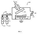
- Fig. 6 is a simplified diagram illustrating an exemplary substrate processing apparatus, such as a DC sputtering apparatus 600, which may be used in accordance with a specific embodiment of the present invention.
- a platinum target 602 (a plate of the platinum material that is to be deposited) is connected to a DC power supply 606 (alternatively, in a RF sputtering system, target 602 is connected to a RF power supply) at a negative voltage and 100 Watt to 200 Watt power while a substrate holder 604 facing target 602 is grounded (as seen in the specific embodiment of Fig. 6) or/and heated by a heater under substrate holder 604.
- An inert gas such as argon in the specific embodiment, is flowed through a gas line 608 at a rate controlled by a mass flow controller 610 into the system from an argon source 612.
- an inert gas can be selected from Ar, Ne, Kr or Xe, in accordance with various specific embodiments.
- Nitrogen also is flowed from a nitrogen source 614 through gas line 608 at a rate controlled by a mass flow controller 616.
- valves 618 are also used for inert gas source 612 and nitrogen source 614.
- a glow discharge When the glow discharge is started, positive ions strike target 602, and target platinum atoms are removed by momentum transfer.
- a sliding shutter 620 is adjusted to expose substrate holder 604, these target platinum atoms subsequently condense into a thin platinum film on a substrate 622, which is on substrate holder 604.
- Target 602 and substrate holder 604 are tilted to each other by about 30° in the specific embodiment.
- Substrate holder 604 rotates during sputter deposition for obtaining uniform platinum film deposition over substrate 622 at a rotating speed of about 3 revolutions per minute, according to the specific embodiment.
- substrate 622 Prior to sputter deposition, substrate 622 was loaded using a magnetic bar into system 600 through a load lock chamber (not shown) coupled to the main chamber containing substrate holder 604.
- the total gas pressure within the main chamber of system 600 is controlled to a set value by exhaust valve 624, which is connected to a pumping system (not shown). Exhaust valve 624 also controls the flow of exhaust from system 600.
- auxiliary electrode is required with the exemplary sputtering deposition system 600 in order to deposit a preferred orientation-controlled platinum film onto substrate 622, which is a silicon substrate in the specific embodiment.
- a magnetron gun may also be used to provide DC/RF magnetron sputtering.
- Exemplary processing conditions and variables for sputter depositing preferred orientation-controlled platinum using an inert gas, such as argon in the specific embodiment, and nitrogen are described as follows.
- the substrate temperature (T S ) which is, more specifically for the specific embodiment, the temperature of the substrate surface during deposition
- the nitrogen content in the gas (F N2 (in %) 100 x (N 2 partial pressure/total gas pressure))
- the film deposition rate (DR (in ⁇ /minute) film thickness ⁇ time spent in film deposition).
- each of the four variables determine many properties of the deposited platinum film, such as preferred orientation, hillock and/or pinhole formation, residual stress in the film, etc.
- each of the four variables preferably should be controlled within some ranges, as discussed generally below.
- Figs. 7a to 7d illustrate the relationship between the degree (in %) of preferred (200) orientation in the deposited platinum film and variation of the above-discussed four deposition process variables.
- Fig. 7a illustrates the effect of changing the substrate temperature T S on the degree of preferred (200) orientation.
- F N2 10 %
- Fig. 7b illustrates the effect of changing the nitrogen content (F N2 ) on the degree of the preferred (200) orientation.
- T S 300°C
- the range of nitrogen content for obtaining preferred (200) orientation is lower than that of the case at a higher T S (500°C), as shown in Fig. 7b.
- Almost 100% of preferred (200) orientation platinum film is obtained for nitrogen content of about 10 % when depositing at a substrate temperature of 300°C.
- almost 100% of preferred (200) orientation platinum film is obtained for nitrogen content of about 35% when depositing at a substrate temperature of 500°C.
- Fig. 7c illustrates the effect of changing the total gas pressure (P tot ) on the degree of the preferred (200) orientation.
- P tot total gas pressure
- F N2 20%
- T S 300°C
- DR 130 ⁇ /min.
- total gas pressure should be in the range of about 1.5-3.0 mTorr in order to obtain close to 100% of preferred (200) orientation platinum film.
- Fig. 7d illustrates the effect of deposition rate on the degree of the preferred (200) orientation.
- preferred ranges for the deposition conditions in the argon and nitrogen deposition atmosphere were found to be as follows: T s of about 300°C to about 500°C; F N2 of about 10-40 %; P tot of about 1.5-3.0 mTorr; and DR of about 80-240 ⁇ /min.
- the preferred ranges for the deposition conditions in the argon and nitrogen deposition atmosphere were found to be as follows: T S of about room temperature to about 200°C; F N2 of about 5-10 %; P tot of about 1.0-1.3 mTorr; and DR of about 80-240 ⁇ /min. Under these processing condition ranges, a preferred (111) orientation-controlled platinum film that was defect-free could be achieved. It was noted that the higher the substrate temperature, the higher the nitrogen content that is required. Further, it was seen that if P tot is too low and the nitrogen content is too high, many hillocks occur on the preferred (111) orientation-controlled platinum film. It was also seen that if P tot is too high and the nitrogen content is too low, many pinholes occur on the preferred (111) orientation-controlled platinum film.
- these four process variables may not be universal (i.e., the value of a certain variable to achieve some property of the film may vary according to the specific substrate processing apparatus used).
- these variables may vary depending on the geometrical factors of chamber volume, target-substrate distance and other properties, such as the magnetic field intensity of the magnetron gun if a magnetron sputtering apparatus is used.
- the annealing conditions are also important for obtaining preferred orientation-controlled and defect-free platinum films.
- the annealing temperature range is preferably from about 400°C to about 1000°C.
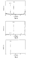
- Figs. 8a to 8f are graphs illustrating X-ray diffraction (XRD) patterns of platinum films deposited in accordance with examples 1 to 6. Typical ⁇ -2 ⁇ scans of the platinum films using Cu K ⁇ radiation in the X-ray diffractometer were performed to find the grains of the platinum films oriented with specific planes, as discussed below in the examples. Figs. 8a to 8f show the XRD intensity in arbitrary units (a.u.) in relation to 2 ⁇ (degrees).
- An insulating layer of SiO 2 was formed on a silicon substrate.
- a platinum film was deposited on the top surface of the insulating layer under an atmosphere containing nitrogen component.
- the platinum film according to the conditions of Example 1 has a mixed (111) and (200) orientation as shown in Fig. 8a.
- Example 2 Deposition was performed under the same conditions as in the Example 1 except that the substrate temperature was 300°C.
- the platinum film has a preferred (200) orientation as shown in Fig. 8b.
- Example 2 Deposition was performed under the same conditions as in the Example 1 except that the substrate temperature was 500°C.
- the platinum film has a preferred (111) orientation as shown in Fig. 8c.
- An insulating layer of SiO 2 was formed on a silicon substrate. Following this, a platinum film was formed on the top surface of the insulating layer under an atmosphere containing nitrogen.
- the platinum film deposited under the above conditions has a preferred (111) orientation as shown in Fig. 8d.
- Example 4 Deposition was performed under the same conditions as in the Example 4 except that the partial pressure ratio of the nitrogen to the entire depositing atmosphere is changed to 20%.
- the platinum film deposited under the above conditions is shown in Fig. 8e.
- the platinum film has a mixed orientation of (111) and (200).
- An insulating layer of SiO 2 was formed on a silicon wafer, a platinum film of 2000 ⁇ thickness was deposited on the insulating layer.
- the platinum film formed in this example has a preferred (220) orientation as shown in Fig. 8f.
- Figs. 9a and 9b are scanning electron microscope micrographs showing a 10,000-times magnified planar view and a 50,000-times magnified cross-sectional view, respectively, of the platinum film deposited by a prior art method.
- a platinum film is coated on a titanium glue layer deposited on a SiO 2 substrate in an argon atmosphere, and then annealed for one hour at 600°C.
- Many white spots observed in Fig. 9a are hillocks or protrusions in the platinum film of the prior art.
- the platinum film of the prior art has a very rough surface as a result of these hillocks.
- Figs. 9a and 9b are scanning electron microscope micrographs showing a 10,000-times magnified planar view and a 50,000-times magnified cross-sectional view, respectively, of the platinum film deposited by a prior art method.
- a platinum film is coated on a titanium glue layer deposited on a SiO 2 substrate in an argon atmosphere, and then annea
- FIG. 9c and 9d are scanning electron microscope micrographs showing 50,000-times magnified planar and cross-sectional views, respectively, of the platinum film deposited by Example 2 according to the present invention.
- the platinum film of a specific embodiment of the present invention appears to be free of hillocks or other defects, as seen in Fig. 9c.
- the cross-sectional view of Fig. 9d demonstrates that the surface of the platinum film is smooth. This example shows that the platinum film deposited by the present invention has no hillocks or any other defects.
- the platinum film formed in the other Examples show the same results, which are not shown to avoid redundancy.
- the platinum film formed according to the present invention is orientation-controllable, and has a dense structure showing no hillocks, pores or buckling, unlike the platinum film formed according to the prior art.
- the platinum films formed in accordance with the present invention show excellent electrical conductivity and the resistivities thereof are lower than 15 ⁇ -cm.
- preferred orientations of platinum films can be controlled by varying at least one of the following parameters: the partial pressure ratio of the nitrogen, the temperature of the substrate during the deposition step, and annealing conditions.
- orientation of the platinum film is controllable by any one of the following parameters: the partial pressure ratio of the nitrogen to the entire platinum deposition atmosphere, the temperature of the substrate during the deposition step, and annealing conditions; it is possible to form a platinum film having desired characteristics for a particular electronic device which uses the platinum film as a bottom electrode.
Landscapes
- Chemical & Material Sciences (AREA)
- Metallurgy (AREA)
- Chemical Kinetics & Catalysis (AREA)
- Engineering & Computer Science (AREA)
- Materials Engineering (AREA)
- Mechanical Engineering (AREA)
- Organic Chemistry (AREA)
- Physics & Mathematics (AREA)
- Thermal Sciences (AREA)
- General Chemical & Material Sciences (AREA)
- Semiconductor Memories (AREA)
- Electrodes Of Semiconductors (AREA)
- Electroplating And Plating Baths Therefor (AREA)
- Electroplating Methods And Accessories (AREA)
Description
- Deposition method: DC magnetron sputtering
- Depositing atmosphere: Ar+N2
- Partial pressure ratio of nitrogen to the entire gas (argon + nitrogen): 10%
- Substrate temperature : room temperature
- Annealing temperature and duration: 600°C for one hour.
- Deposition method: DC magnetron sputtering
- Depositing atmosphere: Ar+N2
- Partial pressure ratio of nitrogen against the entire gas: 5%
- Substrate temperature : 300°C
- Annealing temperature and duration: 650°C for one hour
- Deposition method: DC magnetron sputtering
- Depositing atmosphere: Ar+N2
- Partial pressure of N2 against the entire gas: 30%
- Substrate temperature: 300°C
- Depositing pressure: 1 mTorr
- Annealing temperature and duration: 600°C for one hour
Claims (15)
- A method of forming a platinum film orientation-controlled to (111), (200), and/or (220), comprising the steps of:providing a substrate;forming a functional intermediate film on the substrate;possibly heating the substrate to a temperature;depositing a platinum film on the intermediate layer under an atmosphere containing nitrogen and inert gas, so that the platinum film contains nitrogen; andannealing the platinum film to substantially remove the nitrogen contained in the platinum film, wherein orientation of the platinum film is controlled by at least one of: the partial pressure ratio of the nitrogen to the entire gas in the deposition atmosphere, the temperature of the substrate during the deposition step, and annealing conditions.
- The method of claim 1, wherein the substrate is heated to a temperature of about room temperature to about 500°C.
- The method of claim 1, wherein the inert gas is selected from the group consisting of argon, neon, krypton and xenon.
- The method of claim 1, wherein the partial pressure ratio of the nitrogen to the entire depositing atmosphere gas is less than 50%.
- The method of claim 1, wherein the annealing temperature is about 400°C to 1,000°C.
- The method of claim 1, wherein the substrate is selected from the group of:single component semiconductors such as Si, Ge and C;compound semiconductors such as GaAs, InP, Si/Ge and SiC;single-crystalline ceramic such as SrTiO3, LaAlO3, Al2O3, KBr, NaCl, MgO, ZrO2, Si3N4, TiO2, Ta2O5 and AlN;poly-crystalline ceramic such as Si, SrTiO3, LaAlO3, Al2O3, MgO, KBr, NaCl, ZrO2, Si3N4, TiO2, Ta2O5 and AlN;metals such as Au, Ag, Al, Ir, Pt, Cu, Pd, Ru and W; andnon-crystalline/glassy materials such as BSG, PSG, BPSG and amorphous Si.
- The method of claim 1, wherein the deposition of the platinum film is performed by using any one of DC/RF sputtering, DC/RF magnetron sputtering, metal organic chemical vapor deposition, vacuum evaporation, partially ionized beam deposition, laser ablation.
- The method of claim 1 wherein said method manufactures an electronic device with a bottom electrode comprising the platinum film.
- The method of claim 8, further comprising a step of forming high-dielectric/ferroelectric film on the platinum film.
- The method of claim 9, wherein the functional intermediate film is selected from the group consisting of an insulating layer, a conductive plug layer, an adhesion layer, and a diffusion barrier layer.
- The method of claim 10, wherein the functional intermediate film is an insulating layer and is selected from the group consisting of SiO2, Si3N4, BPSG, BSG, PSG, MgO, CaO, CaF2, Al2O3 or B2O3.
- The method of claim 10, wherein the functional intermediate film is a conductive plug and is formed from a material selected from the group consisting of TiN, zirconium nitride, titanium silicide, tantalum silicide, tungsten silicide, molybdenum silicide, nickel silicide, cobalt silicide, tantalum carbide, tantalum boride, polysilicon, germanium, W, Ta, Ti, Mo, TiW, boron carbide, Cu.
- The method of claim 10, wherein the functional intermediate film is a diffusion barrier layer and is formed from a material selected from the group consisting of ternary component amorphous materials (Ti-Si-N, Ta-B-N, Ti-B-N); conductive nitride (titanium aluminum nitride, Zr nitride, Hf nitride, Y nitride, Se nitride, La nitride and rare earth nitride, N deficient Al nitride, doped Al nitride, Mg nitride, Ca nitride, Sr nitride, Ba nitride, TiN, GaN, Ni nitride, Ta nitride, Co nitride, W nitride).
- The method of claim 10, wherein the functional intermediate film is an adhesion layer and is formed from a material selected from the group comprising TiN, W, Ta, Ti, Sn, Ru, In, Ir, Os, Rh, silicide compound (Ni silicide, Co silicide, W silicide).
- The method of claim 9, wherein the high-dielectric or ferroelectric oxide film is selected from the group consisting of:a perovskite structure oxide such as BT(BaTiO3), BST(Ba1- xSrxTiO3), ST(SrTiO3), PT(PbTiO3), PZT(Pb(Zr, Ti)O3), PLT(Pb1-xLaxTiO3), PLZT((Pb1-xLax)(ZryTiz)1-x/4O3), PMN(PbMg1/3Nb2/3O3), KNbO3, LiTaO3, K(Ta, Nb)O3, CaTiO3, SrSnO3, NaNbO3, LaAlO3, and YAlO3; a bismuth-layered perovskite structure oxide such as SrBiNbO9, SrBi2Ti2O9, SrBi2Ta2O9, SrBi2(TaxNb1-x)2O9 and Bi4Ti3O12; a tungsten-bronze type structure oxide such as Sr1-xBaxNb2O6, (Sr, Ba)0.8RxNa0.4Nb2O6(R: Cr, Zn, Y) , (Pb, Ba)Nb2O6, (K, Sr)Nb2O6, (Pb, K)Nb2O6, Pb2KNb5O15, K3Li2Nb5O15 and (K, Na)3Li2Nb5O15, K2LiNb5O15; ReMnO3 (Re: rare-earth element) ; BaMF4 (M: Mn, Co, Mg, Zn); and KMgF3.
Applications Claiming Priority (4)
| Application Number | Priority Date | Filing Date | Title |
|---|---|---|---|
| KR19970000159 | 1997-01-07 | ||
| KR9700159 | 1997-01-07 | ||
| KR1019970017210A KR19980082338A (en) | 1997-05-06 | 1997-05-06 | Platinum thin film whose orientation is controlled and a method for manufacturing an electronic device having such a platinum thin film and an electronic device provided with a platinum thin film and a platinum thin film formed by the method |
| KR9717210 | 1997-05-06 |
Publications (3)
| Publication Number | Publication Date |
|---|---|
| EP0853336A2 EP0853336A2 (en) | 1998-07-15 |
| EP0853336A3 EP0853336A3 (en) | 1999-06-23 |
| EP0853336B1 true EP0853336B1 (en) | 2002-06-12 |
Family
ID=26632448
Family Applications (1)
| Application Number | Title | Priority Date | Filing Date |
|---|---|---|---|
| EP98400019A Expired - Lifetime EP0853336B1 (en) | 1997-01-07 | 1998-01-07 | Method forming preferred orientation-controlled platinum films using nitrogen |
Country Status (5)
| Country | Link |
|---|---|
| US (1) | US6025205A (en) |
| EP (1) | EP0853336B1 (en) |
| JP (1) | JP3094382B2 (en) |
| KR (1) | KR100262909B1 (en) |
| DE (1) | DE69805865T2 (en) |
Families Citing this family (34)
| Publication number | Priority date | Publication date | Assignee | Title |
|---|---|---|---|---|
| US6312567B1 (en) * | 1996-03-21 | 2001-11-06 | Tong Yang Cement Corporation | Method of forming a (200)-oriented platinum layer |
| US6054331A (en) * | 1997-01-15 | 2000-04-25 | Tong Yang Cement Corporation | Apparatus and methods of depositing a platinum film with anti-oxidizing function over a substrate |
| JP3236793B2 (en) * | 1997-03-28 | 2001-12-10 | 三菱電機株式会社 | Semiconductor memory device having capacitor and method of manufacturing the same |
| KR100269310B1 (en) * | 1997-09-29 | 2000-10-16 | 윤종용 | Semiconductor device using conductive diffusion barrier layer |
| KR100284737B1 (en) * | 1998-03-26 | 2001-03-15 | 윤종용 | Manufacturing method of capacitor having dielectric film of high dielectric constant in semiconductor device |
| TW404021B (en) * | 1998-04-09 | 2000-09-01 | Hitachi Ltd | Semiconductor memory device and manufacturing method thereof |
| JP3159255B2 (en) * | 1998-09-16 | 2001-04-23 | 日本電気株式会社 | Sputter growth method for electrodes used in ferroelectric capacitors |
| US6204158B1 (en) * | 1998-12-18 | 2001-03-20 | Advanced Technology Materials, Inc. | Reduced diffusion of a mobile specie from a metal oxide ceramic into the substrate |
| KR100324591B1 (en) * | 1998-12-24 | 2002-04-17 | 박종섭 | Method for forming capacitor by using TiAIN layer as diffusion barrier of top electrode |
| US6799076B2 (en) * | 1999-12-07 | 2004-09-28 | Greatbatch-Hittman, Inc. | Coated electrode and method of making a coated electrode |
| WO2001088969A2 (en) * | 2000-05-16 | 2001-11-22 | Applied Materials, Inc. | Improved capacitor electrodes |
| US20020003085A1 (en) * | 2000-05-19 | 2002-01-10 | Chandran Ravi R. | Multilayer electrochemical cell technology using sol-gel processing applied to ceramic oxygen generator |
| JP2002151438A (en) * | 2000-09-04 | 2002-05-24 | Nippon Soken Inc | Method for manufacturing semiconductor device |
| US6689687B1 (en) * | 2001-02-02 | 2004-02-10 | Advanced Micro Devices, Inc. | Two-step process for nickel deposition |
| TWI228728B (en) * | 2001-05-29 | 2005-03-01 | Murata Manufacturing Co | Piezoelectric ceramic composition, piezoelectric ceramic element and method for producing piezoelectric ceramic composition |
| KR100522765B1 (en) * | 2001-07-03 | 2005-10-19 | 주식회사 컴텍스 | Manufacturing method of base for semiconductor device using material of GaN series |
| EP1418421A1 (en) * | 2002-11-06 | 2004-05-12 | Ngk Spark Plug Co., Ltd | Gas sensor manufacturing process and sensor |
| US6855647B2 (en) * | 2003-04-02 | 2005-02-15 | Hewlett-Packard Development Company, L.P. | Custom electrodes for molecular memory and logic devices |
| JP4539844B2 (en) * | 2004-04-15 | 2010-09-08 | セイコーエプソン株式会社 | Dielectric capacitor, method of manufacturing the same, and semiconductor device |
| US7616757B2 (en) * | 2004-08-30 | 2009-11-10 | Erdman Joseph L | Scalable call center telecommunications system |
| US8232190B2 (en) * | 2007-10-01 | 2012-07-31 | International Business Machines Corporation | Three dimensional vertical E-fuse structures and methods of manufacturing the same |
| JP5228495B2 (en) * | 2008-01-11 | 2013-07-03 | 富士通セミコンダクター株式会社 | Manufacturing method of semiconductor device |
| CA2717350A1 (en) * | 2008-03-11 | 2009-10-15 | Carnegie Institution Of Washington | New class of pure piezoeletric materials |
| FR2932192B1 (en) * | 2008-06-09 | 2011-01-21 | Sagem Defense Securite | METHOD FOR METALLIZING A VIBRATING CUP AND VIBRANT SENSOR OBTAINED |
| JP5540654B2 (en) * | 2009-11-03 | 2014-07-02 | セイコーエプソン株式会社 | Liquid ejecting head, liquid ejecting apparatus, and piezoelectric element |
| JP5690207B2 (en) * | 2011-05-11 | 2015-03-25 | ルネサスエレクトロニクス株式会社 | Semiconductor device |
| US8574983B2 (en) | 2011-05-13 | 2013-11-05 | Intermolecular, Inc. | Method for fabricating a DRAM capacitor having increased thermal and chemical stability |
| JP5333527B2 (en) | 2011-06-20 | 2013-11-06 | トヨタ自動車株式会社 | Manufacturing method of oxygen sensor |
| JP5799649B2 (en) | 2011-08-10 | 2015-10-28 | トヨタ自動車株式会社 | Manufacturing method of oxygen sensor |
| CN104037120A (en) * | 2013-03-06 | 2014-09-10 | 中芯国际集成电路制造(上海)有限公司 | Method for manufacturing MIM capacitor |
| KR102680283B1 (en) * | 2016-08-29 | 2024-07-03 | 한국재료연구원 | Copper thin layer substrate and fabrication method for the same |
| US11121139B2 (en) * | 2017-11-16 | 2021-09-14 | International Business Machines Corporation | Hafnium oxide and zirconium oxide based ferroelectric devices with textured iridium bottom electrodes |
| JP7426647B2 (en) * | 2019-12-13 | 2024-02-02 | 株式会社デンソー | electret |
| CN115058686B (en) * | 2022-06-17 | 2024-02-20 | 广东风华高新科技股份有限公司 | A preparation method for regulating the crystal growth orientation of Pt film layer |
Family Cites Families (32)
| Publication number | Priority date | Publication date | Assignee | Title |
|---|---|---|---|---|
| US3642548A (en) * | 1969-08-20 | 1972-02-15 | Siemens Ag | Method of producing integrated circuits |
| DE2450551C2 (en) * | 1974-10-24 | 1977-01-13 | Heraeus Gmbh W C | ELECTRICAL RESISTOR FOR A RESISTANCE THERMOMETER AND PROCESS FOR ITS PRODUCTION |
| DE2507731C3 (en) * | 1975-02-22 | 1978-09-07 | Deutsche Gold- Und Silber-Scheideanstalt Vormals Roessler, 6000 Frankfurt | Measuring resistor for resistance thermometer and process for its manufacture |
| US4129848A (en) * | 1975-09-03 | 1978-12-12 | Raytheon Company | Platinum film resistor device |
| US4253931A (en) * | 1979-11-30 | 1981-03-03 | General Motors Corporation | Electrode sputtering process for exhaust gas oxygen sensor |
| US4375056A (en) * | 1980-02-29 | 1983-02-22 | Leeds & Northrup Company | Thin film resistance thermometer device with a predetermined temperature coefficent of resistance and its method of manufacture |
| US4396899A (en) * | 1980-04-16 | 1983-08-02 | Kabushiki Kaisha Kirk | Platinum thin film resistance element and production method therefor |
| US4690861A (en) * | 1985-03-11 | 1987-09-01 | Ricoh Co., Ltd. | Magneto optical recording medium |
| US4966865A (en) * | 1987-02-05 | 1990-10-30 | Texas Instruments Incorporated | Method for planarization of a semiconductor device prior to metallization |
| US4804438A (en) * | 1988-02-08 | 1989-02-14 | Eastman Kodak Company | Method of providing a pattern of conductive platinum silicide |
| US5270252A (en) * | 1988-10-25 | 1993-12-14 | United States Of America As Represented By The Secretary Of The Navy | Method of forming platinum and platinum silicide schottky contacts on beta-silicon carbide |
| US4952904A (en) * | 1988-12-23 | 1990-08-28 | Honeywell Inc. | Adhesion layer for platinum based sensors |
| US5104684A (en) * | 1990-05-25 | 1992-04-14 | Massachusetts Institute Of Technology | Ion beam induced deposition of metals |
| JPH04259380A (en) * | 1991-02-13 | 1992-09-14 | Mitsubishi Materials Corp | Method for controlling crystalline orientation property of pzt ferroelectric body thin film |
| US5142437A (en) * | 1991-06-13 | 1992-08-25 | Ramtron Corporation | Conducting electrode layers for ferroelectric capacitors in integrated circuits and method |
| JPH05235416A (en) * | 1992-02-21 | 1993-09-10 | Murata Mfg Co Ltd | Ferroelectric thin-film element |
| US5191510A (en) * | 1992-04-29 | 1993-03-02 | Ramtron International Corporation | Use of palladium as an adhesion layer and as an electrode in ferroelectric memory devices |
| JPH06108242A (en) * | 1992-09-25 | 1994-04-19 | Minolta Camera Co Ltd | Thin film electrode and apparatus for production of thin film |
| US5514484A (en) * | 1992-11-05 | 1996-05-07 | Fuji Xerox Co., Ltd. | Oriented ferroelectric thin film |
| JPH06196648A (en) * | 1992-12-25 | 1994-07-15 | Fuji Xerox Co Ltd | Oriented ferroelectric thin film device |
| US5348894A (en) * | 1993-01-27 | 1994-09-20 | Texas Instruments Incorporated | Method of forming electrical connections to high dielectric constant materials |
| JPH06305713A (en) * | 1993-04-16 | 1994-11-01 | Texas Instr Japan Ltd | Method for forming ferroelectric film by sol-gel method, method for manufacturing capacitor, and raw material solution thereof |
| JP3412051B2 (en) * | 1993-05-14 | 2003-06-03 | 日本テキサス・インスツルメンツ株式会社 | Capacitor |
| US5320978A (en) * | 1993-07-30 | 1994-06-14 | The United States Of America As Represented By The Secretary Of The Navy | Selective area platinum film deposition |
| US5440173A (en) * | 1993-09-17 | 1995-08-08 | Radiant Technologies | High-temperature electrical contact for making contact to ceramic materials and improved circuit element using the same |
| US5650362A (en) * | 1993-11-04 | 1997-07-22 | Fuji Xerox Co. | Oriented conductive film and process for preparing the same |
| US5585300A (en) * | 1994-08-01 | 1996-12-17 | Texas Instruments Incorporated | Method of making conductive amorphous-nitride barrier layer for high-dielectric-constant material electrodes |
| US5489548A (en) * | 1994-08-01 | 1996-02-06 | Texas Instruments Incorporated | Method of forming high-dielectric-constant material electrodes comprising sidewall spacers |
| US5498569A (en) * | 1994-08-22 | 1996-03-12 | Ramtron International Corporation | Layered local interconnect compatible with integrated circuit ferroelectric capacitors |
| KR0174594B1 (en) * | 1994-11-26 | 1999-04-01 | 이재복 | A method of forming a platinum thin film on a silicon wafer, a silicon substrate manufactured by the method and a semiconductor device using the substrate |
| KR100207444B1 (en) * | 1995-03-14 | 1999-07-15 | 윤종용 | High dielectric film / electrode of semiconductor device and manufacturing method thereof |
| US5650202A (en) * | 1996-07-18 | 1997-07-22 | The United States Of America As Represented By The Secretary Of The Army | Method for forming a platinum coating on non-coductive substrates such as glass |
-
1998
- 1998-01-05 US US09/003,059 patent/US6025205A/en not_active Expired - Fee Related
- 1998-01-07 EP EP98400019A patent/EP0853336B1/en not_active Expired - Lifetime
- 1998-01-07 KR KR1019980000183A patent/KR100262909B1/en not_active Expired - Fee Related
- 1998-01-07 JP JP10031940A patent/JP3094382B2/en not_active Expired - Fee Related
- 1998-01-07 DE DE69805865T patent/DE69805865T2/en not_active Expired - Fee Related
Also Published As
| Publication number | Publication date |
|---|---|
| DE69805865D1 (en) | 2002-07-18 |
| EP0853336A2 (en) | 1998-07-15 |
| JP3094382B2 (en) | 2000-10-03 |
| KR19980070382A (en) | 1998-10-26 |
| KR100262909B1 (en) | 2000-09-01 |
| US6025205A (en) | 2000-02-15 |
| JP2000208723A (en) | 2000-07-28 |
| EP0853336A3 (en) | 1999-06-23 |
| DE69805865T2 (en) | 2003-01-16 |
Similar Documents
| Publication | Publication Date | Title |
|---|---|---|
| US6025205A (en) | Apparatus and methods of forming preferred orientation-controlled platinum films using nitrogen | |
| EP0855738B1 (en) | Method of depositing a platinum film for capacitor electrode | |
| US6498097B1 (en) | Apparatus and method of forming preferred orientation-controlled platinum film using oxygen | |
| US5814852A (en) | Method of forming a Ta2 O5 dielectric layer, method of forming a capacitor having a Ta2 O5 dielectric layer, and capacitor construction | |
| EP1056125B1 (en) | Lead germanate ferroelectric structure with multi-layered electrode | |
| JP4228560B2 (en) | Capacitor element and manufacturing method thereof | |
| EP1101249A1 (en) | Method and apparatus for superior step coverage and interface control for high k dielectric capacitors and related electrodes | |
| US6333537B1 (en) | Thin film capacitor with an improved top electrode | |
| EP1054441A2 (en) | Composite iridium-metal-oxygen barrier structure with refractory metal companion barrier and method for its fabrication | |
| US6291290B1 (en) | Thin film capacitor with an improved top electrode and method of forming the same | |
| KR100262908B1 (en) | Methods of depositing a platinium film with anti-oxidizing function over a substrate and electronic devices incorporating the platinum film | |
| WO2001050509A1 (en) | High dielectric constant material deposition to achieve high capacitance | |
| US20070227877A1 (en) | Magnetron-sputtering film-forming apparatus and manufacturing method for a semiconductor device | |
| US20070096180A1 (en) | Semiconductor device and method for manufacturing the same | |
| KR20010085328A (en) | Vapor growth method for metal oxide dielectric film and vapor growth device for metal oxide dielectric material | |
| JP2002057156A (en) | Vapor phase growth method of metal oxide dielectric film | |
| JP4778136B2 (en) | Semiconductor device and manufacturing method thereof | |
| KR20010045568A (en) | Capacitor manufacturing method for preventing defect generation at subsequent annealing | |
| KR19980082338A (en) | Platinum thin film whose orientation is controlled and a method for manufacturing an electronic device having such a platinum thin film and an electronic device provided with a platinum thin film and a platinum thin film formed by the method | |
| KR19980069763A (en) | Platinum thin film whose orientation is controlled and a method for manufacturing an electronic device having such a platinum thin film and an electronic device provided with a platinum thin film and a platinum thin film formed by the method |
Legal Events
| Date | Code | Title | Description |
|---|---|---|---|
| PUAI | Public reference made under article 153(3) epc to a published international application that has entered the european phase |
Free format text: ORIGINAL CODE: 0009012 |
|
| 17P | Request for examination filed |
Effective date: 19980126 |
|
| AK | Designated contracting states |
Kind code of ref document: A2 Designated state(s): DE FR GB IT NL |
|
| AX | Request for extension of the european patent |
Free format text: AL;LT;LV;MK;RO;SI |
|
| PUAL | Search report despatched |
Free format text: ORIGINAL CODE: 0009013 |
|
| AK | Designated contracting states |
Kind code of ref document: A3 Designated state(s): AT BE CH DE DK ES FI FR GB GR IE IT LI LU MC NL PT SE |
|
| AX | Request for extension of the european patent |
Free format text: AL;LT;LV;MK;RO;SI |
|
| AKX | Designation fees paid |
Free format text: DE FR GB IT NL |
|
| 17Q | First examination report despatched |
Effective date: 20010125 |
|
| GRAG | Despatch of communication of intention to grant |
Free format text: ORIGINAL CODE: EPIDOS AGRA |
|
| GRAG | Despatch of communication of intention to grant |
Free format text: ORIGINAL CODE: EPIDOS AGRA |
|
| GRAH | Despatch of communication of intention to grant a patent |
Free format text: ORIGINAL CODE: EPIDOS IGRA |
|
| GRAH | Despatch of communication of intention to grant a patent |
Free format text: ORIGINAL CODE: EPIDOS IGRA |
|
| GRAA | (expected) grant |
Free format text: ORIGINAL CODE: 0009210 |
|
| AK | Designated contracting states |
Kind code of ref document: B1 Designated state(s): DE FR GB IT NL |
|
| REG | Reference to a national code |
Ref country code: GB Ref legal event code: FG4D |
|
| REF | Corresponds to: |
Ref document number: 69805865 Country of ref document: DE Date of ref document: 20020718 |
|
| ET | Fr: translation filed | ||
| PGFP | Annual fee paid to national office [announced via postgrant information from national office to epo] |
Ref country code: GB Payment date: 20030124 Year of fee payment: 6 |
|
| PGFP | Annual fee paid to national office [announced via postgrant information from national office to epo] |
Ref country code: FR Payment date: 20030127 Year of fee payment: 6 |
|
| PGFP | Annual fee paid to national office [announced via postgrant information from national office to epo] |
Ref country code: NL Payment date: 20030128 Year of fee payment: 6 |
|
| PGFP | Annual fee paid to national office [announced via postgrant information from national office to epo] |
Ref country code: DE Payment date: 20030211 Year of fee payment: 6 |
|
| PLBE | No opposition filed within time limit |
Free format text: ORIGINAL CODE: 0009261 |
|
| STAA | Information on the status of an ep patent application or granted ep patent |
Free format text: STATUS: NO OPPOSITION FILED WITHIN TIME LIMIT |
|
| 26N | No opposition filed |
Effective date: 20030313 |
|
| PG25 | Lapsed in a contracting state [announced via postgrant information from national office to epo] |
Ref country code: GB Free format text: LAPSE BECAUSE OF NON-PAYMENT OF DUE FEES Effective date: 20040107 |
|
| PG25 | Lapsed in a contracting state [announced via postgrant information from national office to epo] |
Ref country code: NL Free format text: LAPSE BECAUSE OF NON-PAYMENT OF DUE FEES Effective date: 20040801 |
|
| PG25 | Lapsed in a contracting state [announced via postgrant information from national office to epo] |
Ref country code: DE Free format text: LAPSE BECAUSE OF NON-PAYMENT OF DUE FEES Effective date: 20040803 |
|
| GBPC | Gb: european patent ceased through non-payment of renewal fee |
Effective date: 20040107 |
|
| PG25 | Lapsed in a contracting state [announced via postgrant information from national office to epo] |
Ref country code: FR Free format text: LAPSE BECAUSE OF NON-PAYMENT OF DUE FEES Effective date: 20040930 |
|
| NLV4 | Nl: lapsed or anulled due to non-payment of the annual fee |
Effective date: 20040801 |
|
| REG | Reference to a national code |
Ref country code: FR Ref legal event code: ST |
|
| PG25 | Lapsed in a contracting state [announced via postgrant information from national office to epo] |
Ref country code: IT Free format text: LAPSE BECAUSE OF NON-PAYMENT OF DUE FEES;WARNING: LAPSES OF ITALIAN PATENTS WITH EFFECTIVE DATE BEFORE 2007 MAY HAVE OCCURRED AT ANY TIME BEFORE 2007. THE CORRECT EFFECTIVE DATE MAY BE DIFFERENT FROM THE ONE RECORDED. Effective date: 20050107 |