EP0851473A2 - Méthode de fabrication d'une couche à constante diélectrique élevée et son application à une couche d'isolation d'une porte et d'un condensateur - Google Patents
Méthode de fabrication d'une couche à constante diélectrique élevée et son application à une couche d'isolation d'une porte et d'un condensateur Download PDFInfo
- Publication number
- EP0851473A2 EP0851473A2 EP97310536A EP97310536A EP0851473A2 EP 0851473 A2 EP0851473 A2 EP 0851473A2 EP 97310536 A EP97310536 A EP 97310536A EP 97310536 A EP97310536 A EP 97310536A EP 0851473 A2 EP0851473 A2 EP 0851473A2
- Authority
- EP
- European Patent Office
- Prior art keywords
- layer
- oxide layer
- recited
- gate
- deposited
- Prior art date
- Legal status (The legal status is an assumption and is not a legal conclusion. Google has not performed a legal analysis and makes no representation as to the accuracy of the status listed.)
- Ceased
Links
Images
Classifications
-
- H—ELECTRICITY
- H01—ELECTRIC ELEMENTS
- H01L—SEMICONDUCTOR DEVICES NOT COVERED BY CLASS H10
- H01L28/00—Passive two-terminal components without a potential-jump or surface barrier for integrated circuits; Details thereof; Multistep manufacturing processes therefor
- H01L28/40—Capacitors
- H01L28/55—Capacitors with a dielectric comprising a perovskite structure material
- H01L28/56—Capacitors with a dielectric comprising a perovskite structure material the dielectric comprising two or more layers, e.g. comprising buffer layers, seed layers, gradient layers
Definitions
- This invention relates to integrated circuits in general and, more particularly, to gate/capacitor dielectrics having a high dielectric constant (high K).
- the threshold voltage of the transistor is correspondingly lowered.
- One approach to lower the threshold voltage is to thin the insulating layer (usually a single layer of silicon dioxide) separating the transistor gate from the transistor channel. But at very thin insulating thicknesses (e.g., an oxide layer thickness of less than 3.5 nm), the oxide layer suffers from pinholes and leakage may be too large. Further, if the oxide layer is less than about 2.5 nm, tunneling of electrons from the transistor channel may occur, degrading transistor performance.
- the gate may be effectively "moved" closer to the channel by incorporating a high dielectric constant (k) material as the gate insulator between the gate and the transistor channel.
- k dielectric constant
- the reduced feature size and lower operating voltage is of special concern with dynamic memories where capacitors are used to store information. As more memory cells are added to a given memory array and feature sizes are decreased so that the extra cells can be added within a reasonable chip size, the size of the storage capacitors are correspondingly decreased. With lower capacitance of the storage capacitors and reduced voltage on the capacitors, the memory may become more error prone. To compensate for the reduction in capacitor size and still maintain capacitance, two approaches can be used singly or in combination: dielectric thinning and increasing the dielectric constant. But the same problems with both approaches discussed above apply here as well.
- the use of high-k materials may be the most desirable choice to solve the above problems at feature sizes of 0.35 ⁇ m and below if the leakage/defects problems can be satisfactorily solved.
- a layer of a high dielectric constant material 4 (referred to herein as a high-k dielectric material), to be described below.
- a high-k dielectric material referred to herein as a high-k dielectric material
- oxide layer 5 is densified.
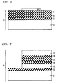
- the wafer 1 includes an exemplary silicon substrate 2 which has grown thereon an oxide layer 3, here a silicon dioxide layer with the silicon coming substantially the substrate 2.
- the layer 3 is preferably grown in a conventional dry oxidizing atmosphere at 0.25 to 10 torr and 650° to 900°C to form 1 to 2 nm thick oxide, the thicknesses not being critical but of sufficient thickness to avoid substantial pinhole formation and a good substrate/oxide interface. While the oxide is preferably grown in a dry atmosphere, it may be grown in a wet (steam) atmosphere.
- the layer 3 is believed to help reduce strain between the later deposited high-k dielectric layer 4 and the underlying silicon substrate 2 and provides a good interface with the silicon to reduce undesired surface states in the silicon. Without the layer 3, it is believed that a lattice mismatch between the substrate 2 and the later deposited layer 4 creates defects at the interface between the layers, decreasing the overall quality of the dielectric.
- a layer or layers 4 of a high-k dielectric material which by way of example may be a ferroelectric dielectric material, this material having a dielectric constant greater than that of silicon dioxide.
- This material may be of group of materials including Ta 2 O 5 , TiO 2 , SrO 3 , and perovskite materials of the form MTiO 3 , where M may be Sr, Ba, La, Ph , Ba x Sr 1-x , and Ph x La 1-x . It is understood that combinations of these layers may be used or interposed insulating layers, such as silicon dioxide, may be added.
- Exemplary thickness of the layer 4 is from 2 to 20 nm and done in a plasma enhanced, ion-beam assisted, or ozone low pressure chemical vapor deposition (LPCVD) or metalorganic chemical vapor deposition (MOCVD) processes. Examples of these processes are as disclosed in "Preparation of (Ba, Sr)TiO3 Thin Films by Chemical Vapor Deposition using Liquid Sources,"by T. Kawahara et al., Japanese Journal of Applied Physics, V33, no. 10, 1994, pp. 5897 - 5902, and "Preparation of PbTiO3 Thin Films by Plasma Enhanced Metalorganic Chemical Vapor Deposition," by E. Fuji et al., Applied Physics Letters, Vol. 65, no. 3, 1994, pp. 365 - 367, included herein by reference.
- LPCVD ozone low pressure chemical vapor deposition
- MOCVD metalorganic chemical vapor deposition
- a layer 5 of silicon dioxide is deposited.
- This layer is preferably 1 to 3 nm thick and preferably formed in a LPCVD reactor (not shown), preferably the same as that used to deposit layer 4.
- Typical source gasses for the silicon include tetraethylorthosilicate gases (TEOS) or silane.
- the layer 5 may be desirably densified by exposing the wafer 1 to a conventional densification anneal process in an oxidizing ambient atmosphere.
- An example of such a process step is in an LPCVD reactor operating at a pressure of 250 millitorr to 10 torr with temperatures between 650° and 900°C for approximately 5 - 20 minutes.
- the oxidizing atmosphere may include N 2 O to add nitrogen to the layer 5.
- the densification step helps improves the overall quality of the layer 5, remove traps (defects) in the layers 3 - 5, and reduces the overall leakage through the layers 3 - 5.
- This layer 6 may be a gate or one plate of a capacitor (the other plate being the substrate 2 or an upper layer not shown), the combination of layers 3 - 5 being referred to herein as a gate or capacitor insulating layer. It is understood that the densification step described above may be done after the formation of layer 6 with the attendant oxidation of the layer 6 if unprotected.
- FIG. 2 An alternative embodiment is shown in FIG. 2 for an exemplary polysilicon-to-polysilicon capacitor structure.
- a wafer 10 has thereon an insulating layer 12 to separate an exemplary oxidizable and conductive layer 13, such as amorphous or polysilicon (the amorphous silicon being rendered conductive at a later step).
- Layers 14 - 16 correspond to layers 3 - 5 in FIG. 1 as described above.
- Layer 17, also preferably a conductive layer, along with layer 13 forms the plates of a capacitor while layers 14-16 form the capacitor insulating layer.
- silicon is described as the material type for the substrate and other layers, it is understood that other materials may be used, such as GaAs, InP, etc.
Applications Claiming Priority (4)
| Application Number | Priority Date | Filing Date | Title |
|---|---|---|---|
| US3384096P | 1996-12-23 | 1996-12-23 | |
| US3383996P | 1996-12-23 | 1996-12-23 | |
| US33840P | 1996-12-23 | ||
| US33839 | 1996-12-23 |
Publications (2)
| Publication Number | Publication Date |
|---|---|
| EP0851473A2 true EP0851473A2 (fr) | 1998-07-01 |
| EP0851473A3 EP0851473A3 (fr) | 1998-07-22 |
Family
ID=26710197
Family Applications (1)
| Application Number | Title | Priority Date | Filing Date |
|---|---|---|---|
| EP97310536A Ceased EP0851473A3 (fr) | 1996-12-23 | 1997-12-23 | Méthode de fabrication d'une couche à constante diélectrique élevée et son application à une couche d'isolation d'une porte et d'un condensateur |
Country Status (1)
| Country | Link |
|---|---|
| EP (1) | EP0851473A3 (fr) |
Cited By (13)
| Publication number | Priority date | Publication date | Assignee | Title |
|---|---|---|---|---|
| EP1020896A1 (fr) * | 1999-01-13 | 2000-07-19 | Lucent Technologies Inc. | Dispositif a circuit intégré avec un diélectrique d'oxyde composite |
| US6235594B1 (en) | 1999-01-13 | 2001-05-22 | Agere Systems Guardian Corp. | Methods of fabricating an integrated circuit device with composite oxide dielectric |
| FR2815773A1 (fr) * | 2000-10-23 | 2002-04-26 | X Ion | Procede de realisation d'un oxyde de grille forme sur substrat semi-conducteur |
| US6392280B1 (en) * | 2000-10-19 | 2002-05-21 | Advanced Micro Devices, Inc. | Metal gate with PVD amorphous silicon layer for CMOS devices and method of making with a replacement gate process |
| US6844604B2 (en) | 2001-02-02 | 2005-01-18 | Samsung Electronics Co., Ltd. | Dielectric layer for semiconductor device and method of manufacturing the same |
| US6969677B2 (en) | 2003-10-20 | 2005-11-29 | Micron Technology, Inc. | Methods of forming conductive metal silicides by reaction of metal with silicon |
| US7026243B2 (en) | 2003-10-20 | 2006-04-11 | Micron Technology, Inc. | Methods of forming conductive material silicides by reaction of metal with silicon |
| US7115532B2 (en) | 2003-09-05 | 2006-10-03 | Micron Technolgoy, Inc. | Methods of forming patterned photoresist layers over semiconductor substrates |
| US7119031B2 (en) | 2004-06-28 | 2006-10-10 | Micron Technology, Inc. | Methods of forming patterned photoresist layers over semiconductor substrates |
| US7153769B2 (en) | 2004-04-08 | 2006-12-26 | Micron Technology, Inc. | Methods of forming a reaction product and methods of forming a conductive metal silicide by reaction of metal with silicon |
| US7241705B2 (en) | 2004-09-01 | 2007-07-10 | Micron Technology, Inc. | Methods of forming conductive contacts to source/drain regions and methods of forming local interconnects |
| US7371633B2 (en) | 2001-02-02 | 2008-05-13 | Samsung Electronics Co., Ltd. | Dielectric layer for semiconductor device and method of manufacturing the same |
| US7384727B2 (en) | 2003-06-26 | 2008-06-10 | Micron Technology, Inc. | Semiconductor processing patterning methods |
Citations (5)
| Publication number | Priority date | Publication date | Assignee | Title |
|---|---|---|---|---|
| JPS6235562A (ja) * | 1985-08-08 | 1987-02-16 | Nec Corp | 半導体装置 |
| JPH02260572A (ja) * | 1989-03-31 | 1990-10-23 | Seiko Epson Corp | 半導体装置 |
| EP0568064A2 (fr) * | 1992-05-01 | 1993-11-03 | Texas Instruments Incorporated | Oxydes à haute constante diélectrique contenant du Pb/Bi utilisant une perovskite ne contenant pas de Pb/Bi comme couche barrière |
| DE4320089A1 (de) * | 1992-06-24 | 1994-01-05 | Gold Star Electronics | Verfahren zum Herstellen eines Kondensators einer Halbleiterspeicherzelle |
| US5444006A (en) * | 1992-11-07 | 1995-08-22 | Goldstar Electron Co., Ltd. | Method of manufacturing a capacitor in a semiconductor memory device |
-
1997
- 1997-12-23 EP EP97310536A patent/EP0851473A3/fr not_active Ceased
Patent Citations (5)
| Publication number | Priority date | Publication date | Assignee | Title |
|---|---|---|---|---|
| JPS6235562A (ja) * | 1985-08-08 | 1987-02-16 | Nec Corp | 半導体装置 |
| JPH02260572A (ja) * | 1989-03-31 | 1990-10-23 | Seiko Epson Corp | 半導体装置 |
| EP0568064A2 (fr) * | 1992-05-01 | 1993-11-03 | Texas Instruments Incorporated | Oxydes à haute constante diélectrique contenant du Pb/Bi utilisant une perovskite ne contenant pas de Pb/Bi comme couche barrière |
| DE4320089A1 (de) * | 1992-06-24 | 1994-01-05 | Gold Star Electronics | Verfahren zum Herstellen eines Kondensators einer Halbleiterspeicherzelle |
| US5444006A (en) * | 1992-11-07 | 1995-08-22 | Goldstar Electron Co., Ltd. | Method of manufacturing a capacitor in a semiconductor memory device |
Non-Patent Citations (2)
| Title |
|---|
| PATENT ABSTRACTS OF JAPAN vol. 011, no. 212 (E-522), 9 July 1987 & JP 62 035562 A (NEC CORP), 16 February 1987, * |
| PATENT ABSTRACTS OF JAPAN vol. 015, no. 004 (E-1020), 8 January 1991 & JP 02 260572 A (SEIKO EPSON CORP), 23 October 1990, * |
Cited By (26)
| Publication number | Priority date | Publication date | Assignee | Title |
|---|---|---|---|---|
| US6235594B1 (en) | 1999-01-13 | 2001-05-22 | Agere Systems Guardian Corp. | Methods of fabricating an integrated circuit device with composite oxide dielectric |
| EP1020896A1 (fr) * | 1999-01-13 | 2000-07-19 | Lucent Technologies Inc. | Dispositif a circuit intégré avec un diélectrique d'oxyde composite |
| US6392280B1 (en) * | 2000-10-19 | 2002-05-21 | Advanced Micro Devices, Inc. | Metal gate with PVD amorphous silicon layer for CMOS devices and method of making with a replacement gate process |
| FR2815773A1 (fr) * | 2000-10-23 | 2002-04-26 | X Ion | Procede de realisation d'un oxyde de grille forme sur substrat semi-conducteur |
| WO2002035609A1 (fr) * | 2000-10-23 | 2002-05-02 | X-Ion | Procede de realisation d'un oxyde de grille forme sur substrat semi-conducteur |
| US7902019B2 (en) | 2001-02-02 | 2011-03-08 | Samsung Electronics Co., Ltd. | Dielectric layer for semiconductor device and method of manufacturing the same |
| US6844604B2 (en) | 2001-02-02 | 2005-01-18 | Samsung Electronics Co., Ltd. | Dielectric layer for semiconductor device and method of manufacturing the same |
| US7371633B2 (en) | 2001-02-02 | 2008-05-13 | Samsung Electronics Co., Ltd. | Dielectric layer for semiconductor device and method of manufacturing the same |
| US7112539B2 (en) | 2001-02-02 | 2006-09-26 | Samsung Electronic Co., Ltd. | Dielectric layer for semiconductor device and method of manufacturing the same |
| US7384727B2 (en) | 2003-06-26 | 2008-06-10 | Micron Technology, Inc. | Semiconductor processing patterning methods |
| US8334221B2 (en) | 2003-09-05 | 2012-12-18 | Micron Technology, Inc. | Methods of forming patterned photoresist layers over semiconductor substrates |
| US7115532B2 (en) | 2003-09-05 | 2006-10-03 | Micron Technolgoy, Inc. | Methods of forming patterned photoresist layers over semiconductor substrates |
| US7985698B2 (en) | 2003-09-05 | 2011-07-26 | Micron Technology, Inc. | Methods of forming patterned photoresist layers over semiconductor substrates |
| US7411254B2 (en) | 2003-10-20 | 2008-08-12 | Micron Technology, Inc. | Semiconductor substrate |
| US7358188B2 (en) | 2003-10-20 | 2008-04-15 | Micron Technology, Inc. | Method of forming conductive metal silicides by reaction of metal with silicon |
| US7026243B2 (en) | 2003-10-20 | 2006-04-11 | Micron Technology, Inc. | Methods of forming conductive material silicides by reaction of metal with silicon |
| US6969677B2 (en) | 2003-10-20 | 2005-11-29 | Micron Technology, Inc. | Methods of forming conductive metal silicides by reaction of metal with silicon |
| US7291555B2 (en) | 2004-04-08 | 2007-11-06 | Micron Technology, Inc. | Methods of forming a reaction product and methods of forming a conductive metal silicide by reaction of metal with silicon |
| US7153769B2 (en) | 2004-04-08 | 2006-12-26 | Micron Technology, Inc. | Methods of forming a reaction product and methods of forming a conductive metal silicide by reaction of metal with silicon |
| US7368399B2 (en) | 2004-06-28 | 2008-05-06 | Micron Technology, Inc. | Methods of forming patterned photoresist layers over semiconductor substrates |
| US7119031B2 (en) | 2004-06-28 | 2006-10-10 | Micron Technology, Inc. | Methods of forming patterned photoresist layers over semiconductor substrates |
| US7241705B2 (en) | 2004-09-01 | 2007-07-10 | Micron Technology, Inc. | Methods of forming conductive contacts to source/drain regions and methods of forming local interconnects |
| US7572710B2 (en) | 2004-09-01 | 2009-08-11 | Micron Technology, Inc. | Methods of forming conductive contacts to source/drain regions and methods of forming local interconnects |
| US7923308B2 (en) | 2004-09-01 | 2011-04-12 | Micron Technology, Inc. | Methods of forming conductive contacts to source/drain regions and methods of forming local interconnects |
| US8084142B2 (en) | 2004-09-01 | 2011-12-27 | Micron Technology, Inc. | Methods of forming conductive contacts to source/drain regions and methods of forming local interconnects |
| US8409933B2 (en) | 2004-09-01 | 2013-04-02 | Micron Technology, Inc. | Methods of forming conductive contacts to source/drain regions and methods of forming local interconnects |
Also Published As
| Publication number | Publication date |
|---|---|
| EP0851473A3 (fr) | 1998-07-22 |
Similar Documents
| Publication | Publication Date | Title |
|---|---|---|
| US20020197790A1 (en) | Method of making a compound, high-K, gate and capacitor insulator layer | |
| US6627503B2 (en) | Method of forming a multilayer dielectric stack | |
| US5780115A (en) | Methods for fabricating electrode structures including oxygen and nitrogen plasma treatments | |
| JP3098474B2 (ja) | 半導体装置の製造方法 | |
| US6998667B2 (en) | Scalable gate and storage dielectric | |
| US5818079A (en) | Semiconductor integrated circuit device having a ceramic thin film capacitor | |
| US20020153579A1 (en) | Semiconductor device with thin film having high permittivity and uniform thickness | |
| EP0926739A1 (fr) | Structure et procédé pour un transistor à effet de champ du type MIS | |
| US5349494A (en) | Semiconductor device with capacitor insulating film and method for fabricating the same | |
| US20050280069A1 (en) | Semiconductor device and method of manufacturing the same | |
| US20050056900A1 (en) | Method and structure for forming high-k gates | |
| EP0851473A2 (fr) | Méthode de fabrication d'une couche à constante diélectrique élevée et son application à une couche d'isolation d'une porte et d'un condensateur | |
| US6235594B1 (en) | Methods of fabricating an integrated circuit device with composite oxide dielectric | |
| US6548854B1 (en) | Compound, high-K, gate and capacitor insulator layer | |
| US6784473B2 (en) | Semiconductor nonvolatile storage element and method of fabricating the same | |
| US6326258B1 (en) | Method of manufacturing semiconductor device having thin film capacitor | |
| KR100947064B1 (ko) | 반도체 장치의 커패시터 및 이를 구비하는 메모리 장치 | |
| JP2005064523A (ja) | 半導体装置のキャパシタとその製造方法、およびそのキャパシタを備えるメモリ装置 | |
| US20050042836A1 (en) | Capacitor for semiconductor device, manufacturing method thereof, and electronic device employing the same | |
| US6670668B2 (en) | Microelectronic structure, method for fabricating it and its use in a memory cell | |
| US6750501B2 (en) | Transistor type ferroelectric body nonvolatile storage element | |
| US6323114B1 (en) | Stacked/composite gate dielectric which incorporates nitrogen at an interface | |
| JPH0513706A (ja) | 半導体装置 | |
| US20010013616A1 (en) | Integrated circuit device with composite oxide dielectric | |
| KR19980064489A (ko) | 혼합된, 높은 k의 게이트와 커패시터 절연층을 만드는 방법과그에 관한 장치 |
Legal Events
| Date | Code | Title | Description |
|---|---|---|---|
| PUAI | Public reference made under article 153(3) epc to a published international application that has entered the european phase |
Free format text: ORIGINAL CODE: 0009012 |
|
| PUAL | Search report despatched |
Free format text: ORIGINAL CODE: 0009013 |
|
| 17P | Request for examination filed |
Effective date: 19980108 |
|
| AK | Designated contracting states |
Kind code of ref document: A2 Designated state(s): DE FR GB IT |
|
| AX | Request for extension of the european patent |
Free format text: AL;LT;LV;MK;RO;SI |
|
| AK | Designated contracting states |
Kind code of ref document: A3 Designated state(s): AT BE CH DE DK ES FI FR GB GR IE IT LI LU MC NL PT SE |
|
| AX | Request for extension of the european patent |
Free format text: AL;LT;LV;MK;RO;SI |
|
| 17Q | First examination report despatched |
Effective date: 19980924 |
|
| AKX | Designation fees paid |
Free format text: DE FR GB IT |
|
| RBV | Designated contracting states (corrected) |
Designated state(s): DE FR GB IT |
|
| APAB | Appeal dossier modified |
Free format text: ORIGINAL CODE: EPIDOS NOAPE |
|
| APAB | Appeal dossier modified |
Free format text: ORIGINAL CODE: EPIDOS NOAPE |
|
| APAD | Appeal reference recorded |
Free format text: ORIGINAL CODE: EPIDOS REFNE |
|
| APBT | Appeal procedure closed |
Free format text: ORIGINAL CODE: EPIDOSNNOA9E |
|
| APBV | Interlocutory revision of appeal recorded |
Free format text: ORIGINAL CODE: EPIDOSNIRAPE |
|
| STAA | Information on the status of an ep patent application or granted ep patent |
Free format text: STATUS: THE APPLICATION HAS BEEN REFUSED |
|
| 18R | Application refused |
Effective date: 20040404 |
|
| APAF | Appeal reference modified |
Free format text: ORIGINAL CODE: EPIDOSCREFNE |