EP0849873A1 - Image-reject mixer arrangements - Google Patents
Image-reject mixer arrangements Download PDFInfo
- Publication number
- EP0849873A1 EP0849873A1 EP97309441A EP97309441A EP0849873A1 EP 0849873 A1 EP0849873 A1 EP 0849873A1 EP 97309441 A EP97309441 A EP 97309441A EP 97309441 A EP97309441 A EP 97309441A EP 0849873 A1 EP0849873 A1 EP 0849873A1
- Authority
- EP
- European Patent Office
- Prior art keywords
- transistors
- pair
- current
- mixer
- image
- Prior art date
- Legal status (The legal status is an assumption and is not a legal conclusion. Google has not performed a legal analysis and makes no representation as to the accuracy of the status listed.)
- Withdrawn
Links
Images


Classifications
-
- H—ELECTRICITY
- H03—ELECTRONIC CIRCUITRY
- H03D—DEMODULATION OR TRANSFERENCE OF MODULATION FROM ONE CARRIER TO ANOTHER
- H03D7/00—Transference of modulation from one carrier to another, e.g. frequency-changing
- H03D7/18—Modifications of frequency-changers for eliminating image frequencies
Definitions
- the present invention relates to image-reject mixer arrangements, and in particular although not exclusively to summing circuits for image-reject mixer arrangements.
- the quadrature output signals from I and Q mixers are shifted in phase relative to one another by a further 90° and summed, the "wanted" components of the I and Q output signals then being in phase and tending to reinforce one another and the image signals being out of phase and tending to cancel.
- the mixer, phase-shift and summing circuits are conventionally designed as discrete circuits each imposing its own bias current demands upon the energising supply.
- current signals corresponding to the I and Q output signals are arranged to be applied by way of respective current mode phase shift circuits to at least one cascode-connected current combining circuit.
- quadrature I and Q output signals from respective mixers are arranged to be applied by way of respective balanced transconductance amplifiers and respective current mode phase shift circuits to at least one cascode-connected current combining circuit.
- an image-reject mixer arrangement comprises, in respect of output signals from each of an I mixer and a Q mixer, an emitter-coupled pair of amplifier transistors to the base electrodes of which the output signals from the respective mixer are applied in antiphase, a current mode phase shifter and a pair of current combining transistors, the collector electrodes of the transistors of each pair of amplifier transistors being connected by way of the respective phase shifter to the emitter electrodes of the respective pair of current combining transistors and the collector electrodes of one pair of current combining transistors being connected to respective ones of the collector electrodes of the other pair of current combining transistors.
- an image-reject mixer arrangement comprises, in respect of output signals from each of an I mixer and a Q mixer, an emitter-coupled pair of amplifier transistors to the base electrodes of which the output signals from the respective mixer are applied in antiphase, and a current mode phase shifter having first and second outputs, the collector electrodes of the transistors of each pair of amplifier transistors being connected by way of the respective phase shifter to the emitter electrodes of a pair of current combining transistors, the emitter electrode of each transistor of said current combining pair of transistors being connected to an output of each of said phase shifters.
- a monolithically formed image-reject mixer arrangement in accordance with any of the above aspects may have a lowermost plate of at least one phase shifter capacitor connected to the emitter electrode of a or the respective current combining transistor.
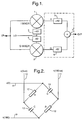
- the local oscillator signals applied to the two mixers are arranged to be in quadrature, for example by utilising respective phase shifters 3 and 4 to shift the phase of signals from a common local oscillator source by plus and minus 45°. If the I and Q output signals are then shifted in phase relative to one another by a further 90°, for example by means of respective plus and minus 45° phase shifters 5 and 6, and added in a summing circuit 7, the signal components of the "wanted" sideband from the two output signals tend to reinforce one another while the signal components of the "image" sideband tend to cancel.
- the phase-shift network shown in Figure 2 receives balanced, i.e. antiphase, signals at inputs 8 and 9 and provides signals at outputs 10 and 11 which are also in antiphase but which are shifted in phase relative to the signals at the inputs 8 and 9 in a sense and by an amount determined by the values of the resistors 12 and the capacitors 13.
- phase shift networks 14 and 15 may be utilised as shown in Figure 3, where antiphase I-channel signals applied by way of emitter-follower circuits 16 and 17 are shifted in phase by plus 45° and passed to an emitter-coupled pair of transistors 18, and antiphase Q-channel signals applied by way of emitter-follower circuits 19 and 20 are shifted in phase by minus 45° and passed to another emitter-coupled pair of transistors 21.
- Current output signals from the collector electrodes of the transistor pairs 18 and 21 are added at outputs 22 and 23.
- each of the emitter followers 16, 17, 19 and 20, and the emitter-coupled pairs 18 and 21 requires its own current source 24.
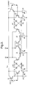
- antiphase I and Q-channel signals are applied to respective emitter-coupled transistor pairs 25 and 26 respectively.
- Current signals from the collector electrodes of these transistor pairs are shifted in phase by plus 45° and minus 45° by respective current mode phase shift networks 27 and 28 and then summed at outputs 33, 34 connected to the collector electrodes of transistors 29, 32 and transistors 30, 31 respectively.
- Transistors 29 and 30 are connected respectively in cascode with the transistors of pair 25, and transistors 31 and 32 are connected respectively in cascode with the transistors of pair 26, a bias potential being applied to the base electrodes of the transistors 29 to 32 over a common path 35. Only two current sources 36 are required, one for each emitter-coupled pair 25, 26, so the present circuit arrangement draws less current from the energising supply (not shown) than the circuit arrangement of Figure 3.
- Figure 5 illustrates a phase shift network for operation in current mode, the network being essentially similar to the voltage-mode network of Figure 2.
- nodes 37 and 38 would be connected respectively to the collector electrodes of the transistors of a pair 25 or 26, while nodes 39 and 40 would be connected respectively to the emitter electrodes of transistors 29 and 30 or 31 and 32.
- antiphase I and Q channel signals are applied to respective emitter-coupled transistor pairs 25 and 26 respectively.
- Current signals from the collector electrodes of these transistor pairs are subsequently shifted in phase by plus 45° and minus 45° by respective current mode phase shift networks 27 and 28.
- the arrangement thusfar described is the same as that shown in Figure 4, from which reference numerals have been retained for like elements.
- current summation is performed at the emitter electrodes of summing transistors 41 and 42.
- the transistors 41, 42 are able to perform the desired summation in this way because their input impedance, defined by their emitter impedance, is substantially lower than the output impedance of the phase shift networks 27, 28.
- the transistors 41, 42 do still however present a high impedance with output signals provided on outputs 43 and 44 because it is defined by the collector impedance of these transistors 41, 42.
- Transistors 41 and 42 are connected in cascode with transistors of both pairs 25 and 26, a bias potential being applied to the base electrodes of the transistors 41 and 42 over a common path 35.
- only two current sources 36 are required, one for each emitter-coupled pair 25, 26, so the present circuit arrangement draws less current from the energising supply (not shown) than the circuit arrangement of Figure 3.
Abstract
Description
Claims (5)
- An image-reject mixer arrangement in which quadrature I and Q output signals from I and Q mixers are arranged to be phase-shifted relative to one another by ninety degrees and summed, wherein current signals corresponding to the I and Q output signals are arranged to be applied by way of respective current mode phase shift circuits to at least one cascode-connected current combining circuit.
- An image-reject mixer arrangement wherein quadrature I and Q output signals from respective mixers are arranged to be applied by way of respective balanced transconductance amplifiers and respective current mode phase shift circuits to at least one cascode-connected current combining circuit.
- An image-reject mixer arrangement comprising, in respect of output signals from each of an I mixer and a Q mixer, an emitter-coupled pair of amplifier transistors to the base electrodes of which the output signals from the respective mixer are applied in antiphase, a current mode phase shifter and a pair of current combining transistors, the collector electrodes of the transistors of each pair of amplifier transistors being connected by way of the respective phase shifter to the emitter electrodes of the respective pair of current combining transistors and the collector electrodes of one pair of current combining transistors being connected to respective ones of the collector electrodes of the other pair of current combining transistors.
- An image-reject mixer arrangement comprising, in respect of output signals from each of an I mixer and a Q mixer, an emitter-coupled pair of amplifier transistors to the base electrodes of which the output signals from the respective mixer are applied in antiphase, and a current mode phase shifter having first and second outputs, the collector electrodes of the transistors of each pair of amplifier transistors being connected by way of the respective phase shifter to the emitter electrodes of a pair of current combining transistors, the emitter electrode of each transistor of said current combining pair of transistors being connected to an output of each of said phase shifters.
- A monolithically formed image-reject mixer arrangement in accordance with any preceding Claim in which a lowermost plate of at least one phase shifter capacitor is connected to the emitter electrode of a or the respective current combining transistor.
Applications Claiming Priority (2)
| Application Number | Priority Date | Filing Date | Title |
|---|---|---|---|
| GB9626229 | 1996-12-18 | ||
| GBGB9626229.0A GB9626229D0 (en) | 1996-12-18 | 1996-12-18 | Image-reject mixer arrangements |
Publications (1)
| Publication Number | Publication Date |
|---|---|
| EP0849873A1 true EP0849873A1 (en) | 1998-06-24 |
Family
ID=10804606
Family Applications (1)
| Application Number | Title | Priority Date | Filing Date |
|---|---|---|---|
| EP97309441A Withdrawn EP0849873A1 (en) | 1996-12-18 | 1997-11-24 | Image-reject mixer arrangements |
Country Status (3)
| Country | Link |
|---|---|
| EP (1) | EP0849873A1 (en) |
| JP (1) | JPH10190359A (en) |
| GB (1) | GB9626229D0 (en) |
Cited By (3)
| Publication number | Priority date | Publication date | Assignee | Title |
|---|---|---|---|---|
| EP1137168A2 (en) * | 2000-03-24 | 2001-09-26 | Nokia Mobile Phones Ltd. | Method and mixer for forming an intermediate frequency signal |
| WO2003050945A2 (en) * | 2001-12-11 | 2003-06-19 | Microtune (Texas), L.P. | Image reject mixer |
| US6999746B2 (en) * | 2000-03-30 | 2006-02-14 | Nec Compound Semiconductor Devices, Ltd. | Image rejection mixer |
Citations (5)
| Publication number | Priority date | Publication date | Assignee | Title |
|---|---|---|---|---|
| EP0488558A1 (en) * | 1990-11-28 | 1992-06-03 | Matsushita Electric Industrial Co., Ltd. | Quadrature detecting apparatus |
| US5140198A (en) * | 1989-08-30 | 1992-08-18 | Seiko Corporation | Image canceling mixer circuit on an integrated circuit chip |
| EP0707379A1 (en) * | 1994-10-11 | 1996-04-17 | BELL TELEPHONE MANUFACTURING COMPANY Naamloze Vennootschap | Tunable quadrature phase shifter |
| EP0715403A1 (en) * | 1994-11-29 | 1996-06-05 | STMicroelectronics Limited | A satellite tuner stage |
| JPH08256187A (en) * | 1995-03-17 | 1996-10-01 | Fujitsu Ltd | Quadrature modulator |
-
1996
- 1996-12-18 GB GBGB9626229.0A patent/GB9626229D0/en active Pending
-
1997
- 1997-11-24 EP EP97309441A patent/EP0849873A1/en not_active Withdrawn
- 1997-12-16 JP JP36358097A patent/JPH10190359A/en active Pending
Patent Citations (5)
| Publication number | Priority date | Publication date | Assignee | Title |
|---|---|---|---|---|
| US5140198A (en) * | 1989-08-30 | 1992-08-18 | Seiko Corporation | Image canceling mixer circuit on an integrated circuit chip |
| EP0488558A1 (en) * | 1990-11-28 | 1992-06-03 | Matsushita Electric Industrial Co., Ltd. | Quadrature detecting apparatus |
| EP0707379A1 (en) * | 1994-10-11 | 1996-04-17 | BELL TELEPHONE MANUFACTURING COMPANY Naamloze Vennootschap | Tunable quadrature phase shifter |
| EP0715403A1 (en) * | 1994-11-29 | 1996-06-05 | STMicroelectronics Limited | A satellite tuner stage |
| JPH08256187A (en) * | 1995-03-17 | 1996-10-01 | Fujitsu Ltd | Quadrature modulator |
Non-Patent Citations (1)
| Title |
|---|
| PATENT ABSTRACTS OF JAPAN vol. 097, no. 002 28 February 1997 (1997-02-28) * |
Cited By (7)
| Publication number | Priority date | Publication date | Assignee | Title |
|---|---|---|---|---|
| EP1137168A2 (en) * | 2000-03-24 | 2001-09-26 | Nokia Mobile Phones Ltd. | Method and mixer for forming an intermediate frequency signal |
| EP1137168A3 (en) * | 2000-03-24 | 2003-10-15 | Nokia Corporation | Method and mixer for forming an intermediate frequency signal |
| US7151919B2 (en) | 2000-03-24 | 2006-12-19 | Nokia Corporation | Method for forming an intermediate frequency signal in a mixer, and a mixer |
| US6999746B2 (en) * | 2000-03-30 | 2006-02-14 | Nec Compound Semiconductor Devices, Ltd. | Image rejection mixer |
| WO2003050945A2 (en) * | 2001-12-11 | 2003-06-19 | Microtune (Texas), L.P. | Image reject mixer |
| WO2003050945A3 (en) * | 2001-12-11 | 2004-02-12 | Microtune Texas Lp | Image reject mixer |
| US7333791B2 (en) | 2001-12-11 | 2008-02-19 | Microtune (Texas), L.P. | Use of an image reject mixer in a forward data channel tuner |
Also Published As
| Publication number | Publication date |
|---|---|
| JPH10190359A (en) | 1998-07-21 |
| GB9626229D0 (en) | 1997-02-05 |
Similar Documents
| Publication | Publication Date | Title |
|---|---|---|
| US6308058B1 (en) | Image reject mixer | |
| KR100387249B1 (en) | Image rejection mixer | |
| US6993310B2 (en) | Current driven polyphase filters and method of operation | |
| US5532637A (en) | Linear low-noise mixer | |
| US7417486B2 (en) | Voltage-current conversion circuit, amplifier, mixer circuit, and mobile appliance using the circuit | |
| US7271647B2 (en) | Active polyphase filter | |
| EP0501827B1 (en) | Multiplying circuit | |
| JP3429840B2 (en) | Four quadrant multiplying circuit and FM receiver having the same | |
| US6456144B2 (en) | Circuit configuration for mixing an input signal and an oscillator signal with one another | |
| EP0434203A2 (en) | Cross-coupled mixer stage for zero IF radio | |
| US6982584B2 (en) | Phase quadrature and slaved working frequency signal generator | |
| US6927629B2 (en) | Differential amplifier having improved balanced and linearity | |
| EP1160717A1 (en) | Analog multiplying circuit and variable gain amplifying circuit | |
| EP0849873A1 (en) | Image-reject mixer arrangements | |
| GB2321353A (en) | Image reject mixer arrangements | |
| US5115212A (en) | Integrable variable-frequency oscillator circuit | |
| US4616186A (en) | FM quadrature demodulator with distortion compensation | |
| US11405001B2 (en) | Image rejection mixer and communication circuit | |
| JPH06177654A (en) | Balanced modulation circuit | |
| JPH1041750A (en) | Gain controlled frequency converter circuit | |
| US6680639B1 (en) | Phase shifting arrangement for generating mutually orthogonal signals | |
| JPH07115329A (en) | Multiplication circuit | |
| JPH0832353A (en) | Frequency mixing circuit | |
| JPH1075158A (en) | Phase shift circuit |
Legal Events
| Date | Code | Title | Description |
|---|---|---|---|
| PUAI | Public reference made under article 153(3) epc to a published international application that has entered the european phase |
Free format text: ORIGINAL CODE: 0009012 |
|
| AK | Designated contracting states |
Kind code of ref document: A1 Designated state(s): DE FR SE |
|
| AX | Request for extension of the european patent |
Free format text: AL;LT;LV;MK;RO;SI |
|
| RAP1 | Party data changed (applicant data changed or rights of an application transferred) |
Owner name: MITEL SEMICONDUCTOR LIMITED |
|
| 17P | Request for examination filed |
Effective date: 19981117 |
|
| AKX | Designation fees paid |
Free format text: DE FR SE |
|
| RBV | Designated contracting states (corrected) |
Designated state(s): DE FR SE |
|
| 17Q | First examination report despatched |
Effective date: 19990906 |
|
| GRAG | Despatch of communication of intention to grant |
Free format text: ORIGINAL CODE: EPIDOS AGRA |
|
| STAA | Information on the status of an ep patent application or granted ep patent |
Free format text: STATUS: THE APPLICATION HAS BEEN WITHDRAWN |
|
| 18W | Application withdrawn |
Withdrawal date: 20010718 |