EP0848223B1 - Vertical heat treatment device - Google Patents
Vertical heat treatment device Download PDFInfo
- Publication number
- EP0848223B1 EP0848223B1 EP96928741A EP96928741A EP0848223B1 EP 0848223 B1 EP0848223 B1 EP 0848223B1 EP 96928741 A EP96928741 A EP 96928741A EP 96928741 A EP96928741 A EP 96928741A EP 0848223 B1 EP0848223 B1 EP 0848223B1
- Authority
- EP
- European Patent Office
- Prior art keywords
- heat
- wafer
- workpiece
- heat treatment
- vertical
- Prior art date
- Legal status (The legal status is an assumption and is not a legal conclusion. Google has not performed a legal analysis and makes no representation as to the accuracy of the status listed.)
- Expired - Lifetime
Links
Images



Classifications
-
- H—ELECTRICITY
- H10—SEMICONDUCTOR DEVICES; ELECTRIC SOLID-STATE DEVICES NOT OTHERWISE PROVIDED FOR
- H10P—GENERIC PROCESSES OR APPARATUS FOR THE MANUFACTURE OR TREATMENT OF DEVICES COVERED BY CLASS H10
- H10P72/00—Handling or holding of wafers, substrates or devices during manufacture or treatment thereof
- H10P72/04—Apparatus for manufacture or treatment
- H10P72/0431—Apparatus for thermal treatment
- H10P72/0432—Apparatus for thermal treatment mainly by conduction
-
- C—CHEMISTRY; METALLURGY
- C23—COATING METALLIC MATERIAL; COATING MATERIAL WITH METALLIC MATERIAL; CHEMICAL SURFACE TREATMENT; DIFFUSION TREATMENT OF METALLIC MATERIAL; COATING BY VACUUM EVAPORATION, BY SPUTTERING, BY ION IMPLANTATION OR BY CHEMICAL VAPOUR DEPOSITION, IN GENERAL; INHIBITING CORROSION OF METALLIC MATERIAL OR INCRUSTATION IN GENERAL
- C23C—COATING METALLIC MATERIAL; COATING MATERIAL WITH METALLIC MATERIAL; SURFACE TREATMENT OF METALLIC MATERIAL BY DIFFUSION INTO THE SURFACE, BY CHEMICAL CONVERSION OR SUBSTITUTION; COATING BY VACUUM EVAPORATION, BY SPUTTERING, BY ION IMPLANTATION OR BY CHEMICAL VAPOUR DEPOSITION, IN GENERAL
- C23C16/00—Chemical coating by decomposition of gaseous compounds, without leaving reaction products of surface material in the coating, i.e. chemical vapour deposition [CVD] processes
- C23C16/44—Chemical coating by decomposition of gaseous compounds, without leaving reaction products of surface material in the coating, i.e. chemical vapour deposition [CVD] processes characterised by the method of coating
- C23C16/46—Chemical coating by decomposition of gaseous compounds, without leaving reaction products of surface material in the coating, i.e. chemical vapour deposition [CVD] processes characterised by the method of coating characterised by the method used for heating the substrate
-
- C—CHEMISTRY; METALLURGY
- C30—CRYSTAL GROWTH
- C30B—SINGLE-CRYSTAL GROWTH; UNIDIRECTIONAL SOLIDIFICATION OF EUTECTIC MATERIAL OR UNIDIRECTIONAL DEMIXING OF EUTECTOID MATERIAL; REFINING BY ZONE-MELTING OF MATERIAL; PRODUCTION OF A HOMOGENEOUS POLYCRYSTALLINE MATERIAL WITH DEFINED STRUCTURE; SINGLE CRYSTALS OR HOMOGENEOUS POLYCRYSTALLINE MATERIAL WITH DEFINED STRUCTURE; AFTER-TREATMENT OF SINGLE CRYSTALS OR A HOMOGENEOUS POLYCRYSTALLINE MATERIAL WITH DEFINED STRUCTURE; APPARATUS THEREFOR
- C30B25/00—Single-crystal growth by chemical reaction of reactive gases, e.g. chemical vapour-deposition growth
- C30B25/02—Epitaxial-layer growth
- C30B25/10—Heating of the reaction chamber or the substrate
-
- C—CHEMISTRY; METALLURGY
- C30—CRYSTAL GROWTH
- C30B—SINGLE-CRYSTAL GROWTH; UNIDIRECTIONAL SOLIDIFICATION OF EUTECTIC MATERIAL OR UNIDIRECTIONAL DEMIXING OF EUTECTOID MATERIAL; REFINING BY ZONE-MELTING OF MATERIAL; PRODUCTION OF A HOMOGENEOUS POLYCRYSTALLINE MATERIAL WITH DEFINED STRUCTURE; SINGLE CRYSTALS OR HOMOGENEOUS POLYCRYSTALLINE MATERIAL WITH DEFINED STRUCTURE; AFTER-TREATMENT OF SINGLE CRYSTALS OR A HOMOGENEOUS POLYCRYSTALLINE MATERIAL WITH DEFINED STRUCTURE; APPARATUS THEREFOR
- C30B31/00—Diffusion or doping processes for single crystals or homogeneous polycrystalline material with defined structure; Apparatus therefor
- C30B31/06—Diffusion or doping processes for single crystals or homogeneous polycrystalline material with defined structure; Apparatus therefor by contacting with diffusion material in the gaseous state
- C30B31/12—Heating of the reaction chamber
-
- F—MECHANICAL ENGINEERING; LIGHTING; HEATING; WEAPONS; BLASTING
- F27—FURNACES; KILNS; OVENS; RETORTS
- F27B—FURNACES, KILNS, OVENS OR RETORTS IN GENERAL; OPEN SINTERING OR LIKE APPARATUS
- F27B17/00—Furnaces of a kind not covered by any of groups F27B1/00 - F27B15/00
- F27B17/0016—Chamber type furnaces
Definitions
- the present invention relates to a vertical heat treatment equipment utilized for oxide film formation, impurity diffusion, or deposit film formation, for example, in the producing process of the wafers of the semiconductor.
- the heat treatment equipment with a heating furnace has conventionally been utilized in the art for operations such as annealing, diffusion of impurities including phosphorus, arsenic and the like, oxide film formation, chemical vapor deposition and the like.
- As one type of the heat treatment equipment there has been provided an equipment of a vertical furnace system wherein one or more wafers of the semiconductor are heated as supported in a horizontal position (see, for example, Japanese Unexamined Patent Publication No.2(1990)-14514).
- this type of heat treatment equipment typically comprises a process chamber 91 adapted for heat treatment of a wafer W of the semiconductor and a carrier chamber 92 disposed under the process chamber 91 for feeding the wafer W thereto or for taking out the heat-treated wafer W therefrom.
- the wafer W of the semiconductor fed to the carrier chamber 92 is supported by a support 93 and transported by elevating means 94 up to a heat-treatment position 91a in the process chamber 91 so as to be subjected to the heat treatment by means of a heating furnace 96 equipped with a heater 95 of a resistance heating system.
- the aforesaid vertical heat treatment equipment known to the art is arranged such that the heater 95 of the heating furnace 96 is concentrated near the top of the process chamber 91 whereby the process chamber 91 has a distribution of temperature, which is the highest at a top 91b of the process chamber and gradually decreases toward the lower portion thereof. This provides an efficient heating of an upper side of the wafer W of the semiconductor.
- the conventional vertical heat treatment equipment particularly right after the start of the heat treatment, fails to assure a processing precision (so-called uniformity) such as of a uniform film thickness of a single wafer W of the semiconductor, as well as a processing precision (so-called repeatability) such as of a uniform film thickness of a plurality of wafers W.
- the heating furnace 96 has the heater 95 concentrated near the top portion of the process chamber 91, and therefore, when the wafer W of the semiconductor is set to the heat-treatment position 91a in the process chamber 91, the wafer W and the support 93 block radiant heat from the heater 95 thereby producing a lower-temperature region extended under the heat-treatment position 91a, as shown by a diagonally shaded area in Fig. 9.
- the lower-temperature region is responsible for change in the thermal history of the wafer W of the semiconductor while the wafer W moves up and down.
- the present invention has been accomplished based on such a finding and has an object to provide a vertical heat treatment equipment assuring the uniformity and repeatability of workpieces.
- US-A-5 407 485 discloses a heat treatment apparatus having heaters arranged laterally with respect to a heat treatment position of a workpiece.
- EP-A-0 538 874 also discloses a heat treatment apparatus having heaters arranged laterally with respect to heat treatment positions of a workpiece.
- the invention provides a vertical heat treatment apparatus as set out in claim 1.
- the heater of the heating furnace is located laterally of the heat-treatment position in the process chamber and therefore, the workpiece and the support are prevented from blocking the radiant heat from the heater, thus producing no lower-temperature region extended under the heat-treatment position.
- This provides a fixed thermal history while the workpiece moves up and down and hence, a good uniformity and repeatability of workpieces is ensured.
- the workpiece is subject to an efficient heat treatment because the process chamber has a distribution in which a heating temperature is at the maximum at the heat-treatment position.
- the lamp heater is utilized for heating the central portion of the workpiece thereby preventing the occurrence of a temperature difference between the central portion and a peripheral portion of the workpiece. Thus is provided a more uniform and more efficient heat treatment of the workpiece.
- the vertical heat treatment equipment further comprises an input-power control section adapted to control power supplied to the lamp heater in accordance with a vertical position of the workpiece so as to maintain a uniform quantity of heat applied to the central and peripheral portions of the workpiece at any different vertical positions.
- the central and peripheral portions of the workpiece can be uniformly heated at any different vertical positions.
- the vertical heat treatment equipment further comprises a gas supply opening disposed at an upper portion of the process chamber for supplying a treatment gas to the workpiece.
- the treatment gas is allowed to flow down directly onto the workpiece via the gas supply opening thereabove and hence, a turbulence of a treatment-gas flow around the workpiece can be prevented even if the workpiece is elevated quickly.
- a gas supply opening disposed at an upper portion of the process chamber for supplying a treatment gas to the workpiece.
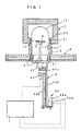
- Fig. 1 is a sectional view for illustrating a vertical heat treatment equipment.
- the vertical heat treatment equipment essentially comprises a process chamber 1 for introducing a wafer W of the semiconductor as a workpiece, a heating furnace 2 for heating the wafer W introduced in the process chamber 1, a wafer support 3 for carrying thereon the wafer W, an elevator 4 for moving up and down the wafer W carried on the wafer support 3, a carrier chamber 5 disposed under the process chamber 1 and adapted to feed the wafer W to the wafer support 3 or to take out the wafer W therefrom, a handling device 6 facing the carrier chamber 5, and a control section 7 for controlling the drive of the elevator 4 and the handling device 6.
- the process chamber 1 comprises a cylinder body 11 having a closed top end and an open bottom end. An upper portion of the cylinder body 11 is enclosed with the heating furnace 2. A side wall 11a of the cylinder body 11 is covered with a heat insulator 12 over a predetermined area of the lower portion thereof.
- the cylinder body 11 is formed of quartz, SiC or the like and has an arched top portion. An opening at the bottom of the cylinder body 11 communicates with the carrier chamber 5, a bottom of which is closed with a bottom plate 51.
- the heating furnace 2 includes a heater 21 of a resistance heating system extended along an inner side of a heating furnace wall 2a.
- the heater 21 is shaped like a coil and disposed laterally of a heat-treatment position 13 for the wafer W of the semiconductor in a manner to surround the heat-treatment position 13 defined at an upper place in the process chamber 1.
- the heater 21 corresponds only to the heat-treatment position 13 such that the process chamber 1 may have a distribution in which a heating temperature is at the maximum at the heat-treatment position 13 and gradually decreases as a vertical distance therefrom increases, as shown in Fig. 2.
- the wafer support 3 comprises a plate-like base 31 such as formed of quartz, SiC or the like and a plurality of support pins 32, such as formed of quartz, upstanding from the base (see Fig. 3).
- the respective support pins 32 have a uniform height so as to support the wafer W of the semiconductor in a horizontal position. Lower ends of the support pins 32 are secured to the base 31.
- the elevator 4 comprises an elevation rod 41 for supporting the wafer support 3, a hydrostatic bearing 42 for vertically movably supporting an intermediate portion of the elevation rod 41, a support member 43 for supporting a lower portion of the elevation rod 41, and a drive section 44 for causing a vertical movement of the support member 43.
- the elevation rod 41 is formed of a quartz tube and has a top end thereof connected with a bottom of the base 31 of the wafer support 3.
- the interior of the elevation rod defines a gas supply passage for supplying a treatment gas to the wafer W of the semiconductor.
- the drive section 44 for causing the vertical movement of the elevation rod 41 comprises a motor 44a, a spiral gear 44b driven by the motor 44a, an elevation member 44c having the support member 43 attached thereto and screwed into the spiral gear 44b, a guide rod 44d for guiding the vertical up-and-down movement of the elevation member 44c, and an encoder 44e for controlling a stroke of the elevation rod 41.
- the handling device 6 comprises a robotic arm 61 adapted to pivot about a vertical shaft, and a suction member 62 disposed at the distal end of the robotic arm 61 and adapted for vacuum suction of the wafer W of the semiconductor.
- the handling device 6 operates to feed a wafer W of the semiconductor onto the support pins 32 from a lateral side of the wafer support 3 or to remove the heat-treated wafer W of the semiconductor from the support pins 32, while the wafer support 3 is down at the carrier chamber 5.
- the above vertical heat treatment equipment is arranged such that the heater 21 of the heating furnace 2 is located laterally of the heat-treatment position 13 for the wafer W of the semiconductor and therefore, the wafer W and the wafer support 3 are prevented from blocking radiant heat from the heater 21, thus producing no low-temperature region extended under the heat-treatment position 13.
- This provides a fixed thermal history of the wafer W while the wafer W moves up and down.
- a processing precision such as of a uniform film thickness of a single wafer W as well as a processing precision such as of a uniform film thickness of a plurality of wafers W, particularly right after the heat treatment has been started.
- the process chamber 1 since the process chamber 1 has a distribution in which a heating temperature is at the maximum at the heat-treatment position 13, the wafers W may be subject to an efficient heat treatment.
- Fig. 4 is a graphical representation of the results of comparison tests of thicknesses of oxide films formed on the wafers of the semiconductor treated by means of the vertical heat treatment equipment according to the above embodiment and the prior-art heat treatment equipment.
- the heat treatment was carried out under the conditions of a dry treatment gas of O 2 , a treatment temperature of 1000°C, and a treatment time of 65 seconds.
- the wafers of the semiconductor having a size of 8 inches were used in the comparison tests.
- As the film thickness data there was found a mean value of measurements at 39 points on a circumference 5-mm inward of the outer circumference of each wafer of the semiconductor.
- the upper lines each denote measurements of the film thicknesses of 25 wafers of the semiconductor sequentially taken one by one over time
- the lower lines each denote variations of the film thickness of a single wafer of the semiconductor in terms of 3 ⁇ ( ⁇ : dispersion).
- the wafers of the semiconductor treated by the vertical heat treatment equipment described above do not suffer the decrease of film thickness which is observed particularly right after the start of the heat treatment. It is also apparent that the variations of the film thickness of a single wafer of the semiconductor treated by the equipment described above are reduced as compared with those of the wafer of the semiconductor treated by the prior-art equipment. Certainly, the equipment described above accomplishes a good uniformity and repeatability of the wafers of the semiconductor.
- the wafer support 3 may adopt a construction comprising two stages vertically arranged and spaced from each other by a predetermined distance, each stage carrying thereon one wafer W of the semiconductor.
- the radiant heat from the heater 21 is unblocked and applied to the wafers of the semiconductor from lateral sides thereof and hence, a positive heat treatment thereof can be accomplished.
- Fig. 5 is a sectional view for illustrating an essential portion of a vertical heat treatment equipment according to an embodiment of the invention.
- This vertical heat treatment equipment differs from that of Fig. 1 in that a quartz glass plate 14 is disposed at an upper side portion of the cylindrical process chamber 1 by way of a metal-formed water-cooling ring 17 containing therein a cooling channel 16 while a lamp heater 8 excellent in directivity, such as an infrared lamp, halogen lamp and the like, is disposed above the central portion of the quartz glass plate 14.
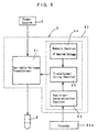
- a power control section 9 is provided for controlling power supplied to the lamp heater 8, and that a plurality of gas supply openings 15 are provided around the lamp heater 8 thereby allowing a treatment gas to flow down directly onto a surface to be treated of the wafer W of the semiconductor.
- the power control section 9 comprises a variable-voltage transformer 91 adapted to transform power supplied from a power source E and to output the power to the lamp heater 8, and a microcomputer 92 for regulating the output power from the variable-voltage transformer 91 based on a signal supplied from the encoder 44e.
- the microcomputer 92 includes a position-determination section 93 responsive to the signal from the encoder 44e to determine a vertical position of the wafer support 3, a memory section of applied voltage 94 containing a voltage to be applied to the lamp heater 8 for each vertical position of the wafer support 3, and a transformer drive section 95 adapted to compare a signal from the position determination section 93 with that from the memory section of applied voltage 94 for providing a real-time variation of the output voltage from the variable voltage transformer 91 in accordance with the vertical position of the wafer support 3.
- the memory section of applied voltage 94 stores an optimum voltage to be applied to the lamp heater 8 for each vertical position of the wafer support 3 so as to constantly maintain a uniform quantity of heat applied to the central and peripheral portions of the wafer W of the semiconductor regardless of any vertical position of the wafer W (see a graphical representation of distribution of synthesized quantity of heats in Fig. 7).
- the vertical heat treatment equipment of this embodiment is adapted to quickly vary the quantity of radiant heat applied to the central portion of the wafer W by way of control of the power to be supplied to the lamp heater 8 by the power control section 9, thus offering a uniform heating of the central and peripheral portions of the wafer W at any different vertical positions.
- the equipment also allows the treatment gas to flow down directly onto the wafer W via the gas supply openings 15 at the upper portion of the process chamber 1. This is effective to prevent the formation of defective crystal and film of ununiform thicknesses as well as to reduce cycle time of the heat treatment of the wafer W. More specifically, without the lamp heater 8, the peripheral portion of the wafer W receives a larger quantity of heat than the central portion thereof, as illustrated by the graphical representation in Fig. 7.
- the peripheral portion of the wafer W is heated faster than the central portion thereof, resulting in a temperature difference between the central portion and the peripheral portion thereof and leading to a greater incidence of defective crystals or a film of ununiform thicknesses.
- the heat-treated wafer W is quickly lowered from the heat-treatment position 13 to the carrier chamber 5, the central portion of the wafer W is cooled faster than the peripheral portion thereof, resulting in a temperature difference between the central portion and the peripheral portion thereof and leading to a greater incidence of defective crystal or a film of ununiform thicknesses.
- the equipment of the above embodiment utilizes the power control section 9 for real-time regulation of the power supplied to the lamp heater 8 in accordance with the vertical position of the wafer W hereby providing a uniform heating of the central and peripheral portions of the wafer W at any different vertical positions. Therefore, the formation of defective crystal or a film of ununiform thicknesses is less likely even if the wafer W is quickly elevated or lowered to the heat-treatment position.
- the equipment of this embodiment provides for the prevention of the formation of the defective crystal and the film of ununiform thicknesses, the assurance of the uniformity and repeatability of the wafers of the semiconductor and the reduction of the cycle time of the heat treatment of the wafers W.
- the vertical heat treatment equipment of the invention is not limited to the aforementioned embodiments.
- the embodiment of the invention shown in Figs. 5 and 6 may be carried out without the power control section 9.
- the lamp heater 8 may be used for heating the central portion of the wafer W set at the heat-treatment position 13 so as to prevent the production of temperature difference between the central portion and the peripheral portion thereof.
- the embodiment of Fig. 1 may also include the lamp heater 8 and the gas supply opening 15 in the upper portion of the process chamber 1.
- the vertical heat treatment equipment of the invention is applicable to heat treatments of other workpieces, such as liquid crystals and the like, besides the aforementioned wafers of the semiconductor.
Landscapes
- Chemical & Material Sciences (AREA)
- Engineering & Computer Science (AREA)
- Materials Engineering (AREA)
- Metallurgy (AREA)
- Organic Chemistry (AREA)
- General Chemical & Material Sciences (AREA)
- Chemical Kinetics & Catalysis (AREA)
- Mechanical Engineering (AREA)
- Crystallography & Structural Chemistry (AREA)
- General Engineering & Computer Science (AREA)
- Chemical Vapour Deposition (AREA)
- Control Of Resistance Heating (AREA)
Description
Claims (3)
- A vertical heat treatment apparatus comprising:a support (3) for carrying thereon a workpiece (W),elevating means (4) for transportation of the workpiece (W) on said support (3) between a carrier chamber (5) and a heat-treatment position in a process chamber (1), anda heating furnace (2) including a heater (21) of a resistance heating system for heating the workpiece (W) transported to said heat-treatment position, wherein said heater (21) is disposed laterally of said heat-treatment position in said process chamber (1) whereby said process chamber (1) has a distribution in which a heating temperature is the highest at said heat-treatment position and gradually decreases as a vertical distance therefrom increases, characterised in that the apparatus further comprises a lamp heater (8) being disposed at an upper place in said process chamber (1) for heating a central portion of the workpiece (W).
- A vertical heat treatment equipment as set forth in claim 1, further comprising a power control section (9) for controlling power supplied to said lamp heater (8) in accordance with a vertical position of the workpiece (W) thereby maintaining a uniform quantity of heat applied to the central and peripheral portions of the workpiece (W) at any different vertical positions.
- A vertical heat treatment equipment as set forth in claim 1 or claim 2, further comprising a gas supply opening (15) disposed at an upper place in said process chamber (1) for supplying a treatment gas to the workpiece (W).
Applications Claiming Priority (4)
| Application Number | Priority Date | Filing Date | Title |
|---|---|---|---|
| JP16537596 | 1996-06-04 | ||
| JP08165375A JP3084232B2 (en) | 1996-06-04 | 1996-06-04 | Vertical heat treatment equipment |
| JP165375/96 | 1996-06-04 | ||
| PCT/JP1996/002484 WO1997046842A1 (en) | 1996-06-04 | 1996-08-30 | Vertical heat treatment device |
Publications (3)
| Publication Number | Publication Date |
|---|---|
| EP0848223A1 EP0848223A1 (en) | 1998-06-17 |
| EP0848223A4 EP0848223A4 (en) | 2000-07-12 |
| EP0848223B1 true EP0848223B1 (en) | 2002-12-04 |
Family
ID=15811185
Family Applications (1)
| Application Number | Title | Priority Date | Filing Date |
|---|---|---|---|
| EP96928741A Expired - Lifetime EP0848223B1 (en) | 1996-06-04 | 1996-08-30 | Vertical heat treatment device |
Country Status (4)
| Country | Link |
|---|---|
| EP (1) | EP0848223B1 (en) |
| JP (1) | JP3084232B2 (en) |
| DE (1) | DE69625212T2 (en) |
| WO (1) | WO1997046842A1 (en) |
Families Citing this family (2)
| Publication number | Priority date | Publication date | Assignee | Title |
|---|---|---|---|---|
| JP4889896B2 (en) * | 2000-11-09 | 2012-03-07 | バッテル メモリアル インスティテュート | Vacuum / gas phase reactor for dehydroxylation and alkylation of porous silica |
| JP6254098B2 (en) * | 2012-02-13 | 2017-12-27 | アプライド マテリアルズ インコーポレイテッドApplied Materials,Incorporated | Method and apparatus for selective oxidation of substrates |
Family Cites Families (13)
| Publication number | Priority date | Publication date | Assignee | Title |
|---|---|---|---|---|
| US3916822A (en) * | 1974-04-26 | 1975-11-04 | Bell Telephone Labor Inc | Chemical vapor deposition reactor |
| JPS61248517A (en) * | 1985-04-26 | 1986-11-05 | Oki Electric Ind Co Ltd | Manufacturing equipment for compound semiconductor thin film |
| JPH0693439B2 (en) * | 1987-03-20 | 1994-11-16 | 株式会社日立製作所 | Semiconductor wafer heat treatment equipment |
| US5156820A (en) * | 1989-05-15 | 1992-10-20 | Rapro Technology, Inc. | Reaction chamber with controlled radiant energy heating and distributed reactant flow |
| US5136978A (en) * | 1989-10-30 | 1992-08-11 | The United States Of America As Represented By The Secretary Of The Air Force | Heat pipe susceptor for epitaxy |
| DE69118513T2 (en) * | 1990-01-19 | 1996-10-02 | Applied Materials Inc | DEVICE FOR HEATING SEMICONDUCTOR DISC OR SUBSTRATES |
| JP2927903B2 (en) * | 1990-07-20 | 1999-07-28 | アネルバ株式会社 | Temperature control method of radiation type substrate heating device |
| JPH0479421U (en) * | 1990-11-22 | 1992-07-10 | ||
| US5387557A (en) * | 1991-10-23 | 1995-02-07 | F. T. L. Co., Ltd. | Method for manufacturing semiconductor devices using heat-treatment vertical reactor with temperature zones |
| JPH05291154A (en) * | 1992-04-06 | 1993-11-05 | Kokusai Electric Co Ltd | Method and device for forming single wafer |
| JPH0613324A (en) * | 1992-06-26 | 1994-01-21 | Fujitsu Ltd | Vacuum heating device |
| JPH06295915A (en) * | 1993-04-09 | 1994-10-21 | F T L:Kk | Semiconductor device manufacturing apparatus and semiconductor device manufacturing method |
| JPH07193020A (en) * | 1993-12-27 | 1995-07-28 | Toshiba Ceramics Co Ltd | Heat treating furnace for semiconductor |
-
1996
- 1996-06-04 JP JP08165375A patent/JP3084232B2/en not_active Expired - Fee Related
- 1996-08-30 WO PCT/JP1996/002484 patent/WO1997046842A1/en not_active Ceased
- 1996-08-30 DE DE69625212T patent/DE69625212T2/en not_active Expired - Fee Related
- 1996-08-30 EP EP96928741A patent/EP0848223B1/en not_active Expired - Lifetime
Also Published As
| Publication number | Publication date |
|---|---|
| JPH09326365A (en) | 1997-12-16 |
| WO1997046842A1 (en) | 1997-12-11 |
| JP3084232B2 (en) | 2000-09-04 |
| EP0848223A1 (en) | 1998-06-17 |
| DE69625212D1 (en) | 2003-01-16 |
| EP0848223A4 (en) | 2000-07-12 |
| DE69625212T2 (en) | 2003-11-13 |
Similar Documents
| Publication | Publication Date | Title |
|---|---|---|
| JP2714577B2 (en) | Heat treatment apparatus and heat treatment method | |
| KR100400488B1 (en) | Method and apparatus for cold wall chemical vapor deposition | |
| US5001327A (en) | Apparatus and method for performing heat treatment on semiconductor wafers | |
| US5775889A (en) | Heat treatment process for preventing slips in semiconductor wafers | |
| KR100241293B1 (en) | Temperature control method and apparatus for high speed heat treatment | |
| US6403927B1 (en) | Heat-processing apparatus and method of semiconductor process | |
| JP3241401B2 (en) | Rapid heat treatment equipment | |
| US5418885A (en) | Three-zone rapid thermal processing system utilizing wafer edge heating means | |
| US5903711A (en) | Heat treatment apparatus and heat treatment method | |
| KR100910292B1 (en) | Heat treatment device | |
| US7432475B2 (en) | Vertical heat treatment device and method controlling the same | |
| US5407485A (en) | Apparatus for producing semiconductor device and method for producing semiconductor device | |
| JPH06302523A (en) | Vertical heat treatment equipment | |
| JP2000323487A (en) | Single wafer heat treatment equipment | |
| JP2668001B2 (en) | Heat treatment method and apparatus | |
| JPH09232297A (en) | Heat treatment equipment | |
| US5626680A (en) | Thermal processing apparatus and process | |
| JPH10233370A (en) | Heat treatment equipment for semiconductor substrates | |
| EP0848223A1 (en) | Vertical heat treatment device | |
| EP0462563B1 (en) | Treating apparatus for semiconductor | |
| JP4157718B2 (en) | Silicon nitride film manufacturing method and silicon nitride film manufacturing apparatus | |
| KR100239405B1 (en) | Semiconductor fabricating system | |
| CN1177830A (en) | Semiconductor wafer heat treatment equipment | |
| JP3507548B2 (en) | Heat treatment method | |
| JP2986739B2 (en) | Heat treatment method in vertical heat treatment device |
Legal Events
| Date | Code | Title | Description |
|---|---|---|---|
| PUAI | Public reference made under article 153(3) epc to a published international application that has entered the european phase |
Free format text: ORIGINAL CODE: 0009012 |
|
| AK | Designated contracting states |
Kind code of ref document: A1 Designated state(s): DE FR GB |
|
| 17P | Request for examination filed |
Effective date: 19980519 |
|
| A4 | Supplementary search report drawn up and despatched |
Effective date: 20000531 |
|
| AK | Designated contracting states |
Kind code of ref document: A4 Designated state(s): DE FR GB |
|
| RIC1 | Information provided on ipc code assigned before grant |
Free format text: 7F 27B 1/09 A, 7H 01L 21/22 B, 7C 30B 31/12 B, 7C 23C 16/46 B, 7C 30B 25/10 B |
|
| RAP1 | Party data changed (applicant data changed or rights of an application transferred) |
Owner name: EATON CORPORATION |
|
| 17Q | First examination report despatched |
Effective date: 20010618 |
|
| GRAG | Despatch of communication of intention to grant |
Free format text: ORIGINAL CODE: EPIDOS AGRA |
|
| GRAG | Despatch of communication of intention to grant |
Free format text: ORIGINAL CODE: EPIDOS AGRA |
|
| GRAH | Despatch of communication of intention to grant a patent |
Free format text: ORIGINAL CODE: EPIDOS IGRA |
|
| RAP1 | Party data changed (applicant data changed or rights of an application transferred) |
Owner name: AXCELIS TECHNOLOGIES, INC. |
|
| GRAH | Despatch of communication of intention to grant a patent |
Free format text: ORIGINAL CODE: EPIDOS IGRA |
|
| GRAA | (expected) grant |
Free format text: ORIGINAL CODE: 0009210 |
|
| AK | Designated contracting states |
Kind code of ref document: B1 Designated state(s): DE FR GB |
|
| REG | Reference to a national code |
Ref country code: GB Ref legal event code: FG4D |
|
| REF | Corresponds to: |
Ref document number: 69625212 Country of ref document: DE Date of ref document: 20030116 |
|
| ET | Fr: translation filed | ||
| PLBE | No opposition filed within time limit |
Free format text: ORIGINAL CODE: 0009261 |
|
| STAA | Information on the status of an ep patent application or granted ep patent |
Free format text: STATUS: NO OPPOSITION FILED WITHIN TIME LIMIT |
|
| 26N | No opposition filed |
Effective date: 20030905 |
|
| PGFP | Annual fee paid to national office [announced via postgrant information from national office to epo] |
Ref country code: DE Payment date: 20070831 Year of fee payment: 12 |
|
| PGFP | Annual fee paid to national office [announced via postgrant information from national office to epo] |
Ref country code: GB Payment date: 20070705 Year of fee payment: 12 |
|
| PGFP | Annual fee paid to national office [announced via postgrant information from national office to epo] |
Ref country code: FR Payment date: 20070803 Year of fee payment: 12 |
|
| GBPC | Gb: european patent ceased through non-payment of renewal fee |
Effective date: 20080830 |
|
| REG | Reference to a national code |
Ref country code: FR Ref legal event code: ST Effective date: 20090430 |
|
| PG25 | Lapsed in a contracting state [announced via postgrant information from national office to epo] |
Ref country code: FR Free format text: LAPSE BECAUSE OF NON-PAYMENT OF DUE FEES Effective date: 20080901 Ref country code: DE Free format text: LAPSE BECAUSE OF NON-PAYMENT OF DUE FEES Effective date: 20090303 |
|
| PG25 | Lapsed in a contracting state [announced via postgrant information from national office to epo] |
Ref country code: GB Free format text: LAPSE BECAUSE OF NON-PAYMENT OF DUE FEES Effective date: 20080830 |