EP0843955B1 - Method of forming raised metallic contacts on electrical circuits - Google Patents
Method of forming raised metallic contacts on electrical circuits Download PDFInfo
- Publication number
- EP0843955B1 EP0843955B1 EP97923639A EP97923639A EP0843955B1 EP 0843955 B1 EP0843955 B1 EP 0843955B1 EP 97923639 A EP97923639 A EP 97923639A EP 97923639 A EP97923639 A EP 97923639A EP 0843955 B1 EP0843955 B1 EP 0843955B1
- Authority
- EP
- European Patent Office
- Prior art keywords
- conductive layer
- dielectric material
- layer
- base substrate
- copper
- Prior art date
- Legal status (The legal status is an assumption and is not a legal conclusion. Google has not performed a legal analysis and makes no representation as to the accuracy of the status listed.)
- Expired - Lifetime
Links
Images


Classifications
-
- H—ELECTRICITY
- H05—ELECTRIC TECHNIQUES NOT OTHERWISE PROVIDED FOR
- H05K—PRINTED CIRCUITS; CASINGS OR CONSTRUCTIONAL DETAILS OF ELECTRIC APPARATUS; MANUFACTURE OF ASSEMBLAGES OF ELECTRICAL COMPONENTS
- H05K3/00—Apparatus or processes for manufacturing printed circuits
- H05K3/40—Forming printed elements for providing electric connections to or between printed circuits
- H05K3/4007—Surface contacts, e.g. bumps
-
- H—ELECTRICITY
- H01—ELECTRIC ELEMENTS
- H01L—SEMICONDUCTOR DEVICES NOT COVERED BY CLASS H10
- H01L2924/00—Indexing scheme for arrangements or methods for connecting or disconnecting semiconductor or solid-state bodies as covered by H01L24/00
- H01L2924/0001—Technical content checked by a classifier
- H01L2924/0002—Not covered by any one of groups H01L24/00, H01L24/00 and H01L2224/00
-
- H—ELECTRICITY
- H05—ELECTRIC TECHNIQUES NOT OTHERWISE PROVIDED FOR
- H05K—PRINTED CIRCUITS; CASINGS OR CONSTRUCTIONAL DETAILS OF ELECTRIC APPARATUS; MANUFACTURE OF ASSEMBLAGES OF ELECTRICAL COMPONENTS
- H05K2201/00—Indexing scheme relating to printed circuits covered by H05K1/00
- H05K2201/03—Conductive materials
- H05K2201/0332—Structure of the conductor
- H05K2201/0364—Conductor shape
- H05K2201/0367—Metallic bump or raised conductor not used as solder bump
-
- H—ELECTRICITY
- H05—ELECTRIC TECHNIQUES NOT OTHERWISE PROVIDED FOR
- H05K—PRINTED CIRCUITS; CASINGS OR CONSTRUCTIONAL DETAILS OF ELECTRIC APPARATUS; MANUFACTURE OF ASSEMBLAGES OF ELECTRICAL COMPONENTS
- H05K2203/00—Indexing scheme relating to apparatus or processes for manufacturing printed circuits covered by H05K3/00
- H05K2203/03—Metal processing
- H05K2203/0338—Transferring metal or conductive material other than a circuit pattern, e.g. bump, solder, printed component
-
- H—ELECTRICITY
- H05—ELECTRIC TECHNIQUES NOT OTHERWISE PROVIDED FOR
- H05K—PRINTED CIRCUITS; CASINGS OR CONSTRUCTIONAL DETAILS OF ELECTRIC APPARATUS; MANUFACTURE OF ASSEMBLAGES OF ELECTRICAL COMPONENTS
- H05K3/00—Apparatus or processes for manufacturing printed circuits
- H05K3/10—Apparatus or processes for manufacturing printed circuits in which conductive material is applied to the insulating support in such a manner as to form the desired conductive pattern
- H05K3/20—Apparatus or processes for manufacturing printed circuits in which conductive material is applied to the insulating support in such a manner as to form the desired conductive pattern by affixing prefabricated conductor pattern
- H05K3/205—Apparatus or processes for manufacturing printed circuits in which conductive material is applied to the insulating support in such a manner as to form the desired conductive pattern by affixing prefabricated conductor pattern using a pattern electroplated or electroformed on a metallic carrier
-
- H—ELECTRICITY
- H05—ELECTRIC TECHNIQUES NOT OTHERWISE PROVIDED FOR
- H05K—PRINTED CIRCUITS; CASINGS OR CONSTRUCTIONAL DETAILS OF ELECTRIC APPARATUS; MANUFACTURE OF ASSEMBLAGES OF ELECTRICAL COMPONENTS
- H05K3/00—Apparatus or processes for manufacturing printed circuits
- H05K3/30—Assembling printed circuits with electric components, e.g. with resistor
- H05K3/32—Assembling printed circuits with electric components, e.g. with resistor electrically connecting electric components or wires to printed circuits
- H05K3/34—Assembling printed circuits with electric components, e.g. with resistor electrically connecting electric components or wires to printed circuits by soldering
- H05K3/3457—Solder materials or compositions; Methods of application thereof
- H05K3/3473—Plating of solder
-
- H—ELECTRICITY
- H05—ELECTRIC TECHNIQUES NOT OTHERWISE PROVIDED FOR
- H05K—PRINTED CIRCUITS; CASINGS OR CONSTRUCTIONAL DETAILS OF ELECTRIC APPARATUS; MANUFACTURE OF ASSEMBLAGES OF ELECTRICAL COMPONENTS
- H05K3/00—Apparatus or processes for manufacturing printed circuits
- H05K3/46—Manufacturing multilayer circuits
- H05K3/4644—Manufacturing multilayer circuits by building the multilayer layer by layer, i.e. build-up multilayer circuits
-
- Y—GENERAL TAGGING OF NEW TECHNOLOGICAL DEVELOPMENTS; GENERAL TAGGING OF CROSS-SECTIONAL TECHNOLOGIES SPANNING OVER SEVERAL SECTIONS OF THE IPC; TECHNICAL SUBJECTS COVERED BY FORMER USPC CROSS-REFERENCE ART COLLECTIONS [XRACs] AND DIGESTS
- Y10—TECHNICAL SUBJECTS COVERED BY FORMER USPC
- Y10S—TECHNICAL SUBJECTS COVERED BY FORMER USPC CROSS-REFERENCE ART COLLECTIONS [XRACs] AND DIGESTS
- Y10S438/00—Semiconductor device manufacturing: process
- Y10S438/977—Thinning or removal of substrate
-
- Y—GENERAL TAGGING OF NEW TECHNOLOGICAL DEVELOPMENTS; GENERAL TAGGING OF CROSS-SECTIONAL TECHNOLOGIES SPANNING OVER SEVERAL SECTIONS OF THE IPC; TECHNICAL SUBJECTS COVERED BY FORMER USPC CROSS-REFERENCE ART COLLECTIONS [XRACs] AND DIGESTS
- Y10—TECHNICAL SUBJECTS COVERED BY FORMER USPC
- Y10T—TECHNICAL SUBJECTS COVERED BY FORMER US CLASSIFICATION
- Y10T29/00—Metal working
- Y10T29/49—Method of mechanical manufacture
- Y10T29/49002—Electrical device making
- Y10T29/49117—Conductor or circuit manufacturing
- Y10T29/49124—On flat or curved insulated base, e.g., printed circuit, etc.
- Y10T29/49126—Assembling bases
Definitions
- the present invention generally relates to the manufacture of electrical circuitry with features having a three-dimensional configuration that extends in one or more directions from a plane of the circuit.
- the connectors of these patents embody a substrate having traces chemically milled thereon with a plurality of metallic raised features later formed to project from the plane of the circuit conductors.
- the connectors when two such connectors are placed face to face, with the raised features of one in registration and contact with the other, the planes of the etched electrical circuits are suitably spaced from one another because of the projection of the features.
- the two circuits may be physically clamped together to press the features against one another, thereby making firm and intimate electrical contact between the two circuits.
- the substantially planar circuitry is chemically milled or etched on the copper surfaces (the panel may often be covered with a coating of copper on both sides for a double sided panel).
- the etching process involves application of photoresist, masking the resist, exposing the resist, developing the resist, then etching through the portions of the copper not protected by the resist so that upon stripping of the remaining resist, the circuit pattern of the copper conductors remains.
- the projecting interconnection features or bumps may be formed first, before the remainder of the etched circuit is formed. But, in any event, the feature must be formed separately, at a different time than the time of forming the etched circuitry, and thus the registration problems are created or exacerbated.
- United States Patent 5,197,184 teaches a method of additively forming three-dimensional electrical circuitry having raised contact buttons without employing circuit etching processes.
- the three-dimensional electrical circuitry is made by fully additive processes employing a circuit mandrel.
- the mandrel comprises a substrate having a working surface formed of a material on which can be electroformed an electrically conductive element, with the mandrel having a first feature projecting in directions perpendicular to the working surface to enable a three-dimensional electrical circuit to be formed by a single electroforming operation.
- the mandrel bears a pattern formed of electrically non-conductive material.
- the entire three-dimensional circuitry of traces and raised interconnection features may be electrodeposited in a single step, all without any photolithographic or etching processes.
- a final step in such a method includes separating the substrate and the circuitry from the mandrel to provide a dielectric substrate having a pattern of circuit traces thereon, including rigid projecting conductive contact buttons configured and arranged to be pressed against contact of another electrical circuit.
- the final process step in the method described in United States Patent 5,197,184 requires the mechanical separation of the substrate and the circuitry from the mandrel. This separation process may be difficult to accomplish without imparting physical damage to the substrate and the circuitry. The stresses imparted to the substrate and the circuitry during this separation may be large enough to cause a change in the dimensions of the substrate. This dimensional change may result in the inability to align all of the bumps on the substrate to their opposing pads on the mating circuit.
- a further shortcoming of the method described in United States Patent 5,197,184 is that the final shape, and particularly the height of the bumps, is completely dependent upon the chemical etching process. Control of the height of the bumps must be determined by the size of the base of the bumps. If bumps of significant height are required, the base must be made large, thus limiting the density of the bump pattern.
- the present invention advances the art of forming three-dimensional metallic contacts, or bumps, on an electrical circuit, beyond which is known to date.
- the method comprises the following steps:
- At least a second dielectric material may be laminated to a first planar surface of said composite base substrate.
- At least a third conductive layer may be laminated to the second dielectric material.
- the third conductive layer may be electrically connected to the first conductive layer.
- the base substrate may be laminated to a printed circuit board.
- Figures 1-16 illustrate a process for forming raised metallic contacts, or bumps, on electrical circuits.
- Figures 1-16 depict a process for forming raised metallic contacts on a two layer electrical circuit, any number of circuit layers may be formed utilizing the teachings of the present invention.
- a base substrate 10 is provided which is defined by a laminate comprised of a conductive layer 12 (such as copper, for example), a dielectric layer 14, and a conductive layer 16 (such as copper, for example).
- the dielectric layer 14 must not comprise a material which is resistant to etching by a laser or plasma process, such as a glass reinforced dielectric layer or a dielectric layer reinforced with ceramic particles.
- Suitable dielectric materials include, but are not limited to polyimides and polyimide laminates, epoxy resins, organic materials, or dielectric materials comprised at least in part of polytetrafluoroethylene.
- a preferred dielectric material may be obtained from W.L. Gore & Associates, Inc. under the tradename SPEEDBOARDTM dielectric materials.
- the thickness of the dielectric layer 14 is important. This thickness will define the height of the resulting raised metallic contacts which are formed by the teachings herein. Additional detail on the significance of dielectric layer 14 will be described below.
- Photoresist 18 is applied to copper layers 12 and 16, respectively, and is processed in a conventional manner to form openings on copper layer 12 where the raised metallic contacts are to be formed.
- the copper in an exposed area 20 is etched away by any suitable conventional copper etchant, such as a cupric chloride based etchant solution.
- Figure 2 illustrates the base substrate 10 after the copper within the exposed area 20 has been etched away. An exposed portion 22 of dielectric layer 14 is shown. The photoresist 18 may then be removed from the substrate.
- the exposed dielectric portion 22 is ablated away with a laser to define a "well" 24 into which a metallic contact will be formed, as shown in Figure 3.
- the copper layer 12 functions as a mask to permit ablation of the exposed dielectric portion 22.
- the copper layer 16 acts as a stop and will define the bottom of the well 24.
- the ablation of the exposed dielectric portion 22 may be accomplished by any laser suitable for selective ablation of organic dielectrics, without removing a copper layer.
- Lasers which operate in ultra violet wavelengths are particularly well suited, such as excimer lasers, and frequency tripled or quadrupled YAG lasers. However, other types of lasers are also suitable.
- the laser may be operated either in a scanning mode, in which the surface of the substrate is swept with a large laser spot, or in a focused beam.
- other processes may be employed to selectively remove the exposed dielectric portion 22, such as but not limited to plasma etching, reactive ion etching, or chemical etching.
- a laser ablation process is particularly well suited, as it permits more control over the shape of the well 24. Simple diffraction will provide a tapered conical shape in the case of scanning mode laser ablation process.
- the base substrate 10 is processed in any suitable manner which deposits a surface conductive layer 26, such as copper, on the side walls of the well 24.
- a surface conductive layer 26 such as copper
- Suitable processes include, but are not limited to a conventional electroless copper plating operation, sputtering, evaporation, or deposition of a conductive coating which allows direct electrodeposition, or any other suitable process. Additional electrolytically deposited copper may be added to thicken this deposit, thereby providing a more robust surface for additional process steps.
- Figure 4 illustrates the base substrate 10 after this conductive deposition step.
- the base substrate 10 is then coated with photoresist 28 on both sides of the base substrate, and the photoresist is processed to define patterns on conductive layer 12, into which additional metal is deposited to simultaneously form at least one metal "bump" contacts and traces for an electric circuit.
- a sacrificial layer of nickel 30 is first deposited to act as a diffusion barrier during subsequent lamination operations.
- a layer of gold 31, which will ultimately form the top layer of the bump contact is then deposited.
- a second layer of nickel 34 is deposited to form a diffusion barrier.
- a layer of copper 36, which will comprise the bulk of the metal, is then deposited.
- Figure 5 illustrates a substrate with the metals deposited as described.
- the photoresist 28 is removed from the base substrate 10.
- the base substrate 10 may then be treated in a conventional oxide process, such as is common in the production of printed circuits.
- the rough oxide formed on the surface of the exposed copper of the base substrate will serve to provide adequate adhesion of the metal to a dielectric material in subsequent lamination processes.
- a layer of a dielectric prepreg material 33, and a "cap" layer of copper 32 may be laminated onto the base substrate 10.
- the temperature, pressure, and time required for the lamination process should be as specified by the manufacturer of the particular dielectric prepreg used.
- This copper layer 32 will form the base for a second metal layer of the electric circuit.
- the dielectric prepreg material may be similar to that used to form the dielectric layer 14. During this lamination process, resin from the dielectric prepreg material 33 will flow into and fill the void space remaining in the well 24.
- FIG. 7 illustrates a via 40 which is formed to interconnect the top conductive layer 32 to the conductive layer 12.
- Via 40 is formed using the same process as described for the formation of the well 24, except that the deposition of the contact and diffusion barrier metals are not necessary.
- the top metal layer of the base substrate is then coated with photoresist 42.
- Conductive layer 16 is then etched away using a suitable etchant.
- Figure 8 illustrates base substrate 10 after the bottom conductive layer 16 has been etched. The photoresist 42 is then removed from conductive layer 16.
- the now exposed dielectric material 14 is removed by any suitable process which will selectively remove dielectric from a conductor such as copper. Suitable processes include but are not limited to plasma etching, laser ablation, reactive ion etching, or chemical etching. Care must be taken that all of the dielectric material 14 is removed from the conductive layer 12, as any remaining dielectric material 14 will prevent the conductive layer 12 from being etched away in subsequent process steps.
- Figure 9 depicts the base substrate 10 after the dielectric material 14 has been removed.
- the top layer of the base substrate 10 is then coated with photoresist to protect it from the etchant which is used to remove the exposed conductive layer 12 and surface conductive layer 26.
- Any suitable etchant may be employed. It may be desirable to employ an etchant that will not only remove the conductive layers 12 and 26, but also the sacrificial nickel layer 30, such as cupric chloride, for example. However, the cupric chloride etchant will not etch the gold beneath the nickel, thus, and in this embodiment of the present invention, a copper/nickel/gold metallurgy remains to form the metallurgy for a bump 50, as well as the metallurgy of the interconnecting traces.
- the photoresist may then be removed from the circuit.
- Figure 10 illustrates a finished circuit made in accordance with the teachings of one embodiment of the present invention.
- the height of the bump 50 is determined by the thickness of the dielectric layer 14, minus the sum of the thickness of the copper layer 12, the surface conductive copper layer 24, and the diffusion barrier of nickel 30.
- the bump height is largely determined by the thickness of the dielectric layer 14.
- dielectrics available today offer thickness control of +/-10% or better, thus the planarity of the bumps created will approach +/-10%.
- the ability to control the bump height by controlling the thickness of the dielectric layer 14, and the degree of planarity achievable by this method is a significant improvement over the method of etching depressions in a mandrel, as described in U.S. Patent 5,197,184.
- process steps are described which permit a base substrate 10, with raised metallic contacts 50, to be laminated and electrically connected to a multilayer circuit board.
- the base substrate 10 is shown as made by the process steps which are described referencing Figures 1-5.
- the base substrate 10 is laminated to a multilayer circuit board 80 with a dielectric prepreg material, as best seen by reference to Figure 12.
- the temperature, pressure, and time required for the lamination process should be as specified by the manufacturer of the particular dielectric prepreg used.
- the multilayer circuit board may have any number of configurations. However, the side which is to be laminated to the base substrate 10 must have a series of pads 60 arranged such that vias 40 may later connect these pads to the base substrate 10, as best seen by sequentially viewing Figures 12-16.
- the opposite side of the multilayer circuit board may be finished prior to lamination, or may have only an unfinished copper layer, in which case this layer will be finished at the same time as the side with the raised contacts.
- the top metal layer of the multi-layer circuit board 80 is then coated with photoresist to protect it from an etchant which is used to etch the conductive layer 16 from the base substrate 10. Any suitable etchant may be used.
- the photoresist is then removed from the multi-layer circuit board 80.
- the now exposed dielectric material 14 is removed by any suitable process for removing a dielectric material from a conductor, such as copper, to thereby expose the raised metallic contacts 50, as best seen in Figure 13.
- a suitable process may include, but is not limited to a plasma etching process, laser ablation, reactive ion etching, or chemical etching, for example. Care must be taken to remove all of the dielectric material from the conductive surface, as any remaining dielectric material will prevent the conductive material from being etched in subsequent process steps.
- the top layer of the multi-layer circuit board 80 is then coated with photoresist to protect it from the etchant which is used to remove the exposed conductive layer 12.
- Any suitable etchant may be employed. It may be desirable to employ an etchant that will not only remove the conductive layer 12, but also the sacrificial nickel layer 30, such as cupric chloride, for example. However, the cupric chloride etchant will not etch the gold beneath the nickel, thus, and in this embodiment of the present invention, a copper/nickel/gold metallurgy remains to form the metallurgy for a bump 50, as well as the metallurgy of the interconnecting traces.
- the photoresist may then be removed from the circuit.
- Figure 13 illustrates a finished circuit made in accordance with the teachings of the present invention.
- Vias 40 are then drilled in the base substrate 10 for circuit interconnection. These vias may be either blind or through vias.
- the base substrate 10 is then processed in a conventional electroless copper plating operation such as is common in printed and flexible circuit manufacturing operations.
- the electroless copper deposits a layer of copper on the base substrate 10 and on the surface of the side walls of the vias. Additional electrolytically deposited copper may be added to thicken the deposit, and provide a more robust surface for additional process steps.
- Figure 14 illustrates the base substrate 10 after such copper deposition.
- any suitable process which deposits a conductor may be used in place of the electroless copper process, such as but not limited to sputtering, evaporation, or deposition of a conductive coating which allows direct electrodeposition.
- the base substrate is then coated with photoresist 28 on both sides, and the photoresist is processed to define patterns into which additional metal is deposited to form via and pad connections. Additional copper would likely be deposited. Also, a final etch resistant metal such as nickel, gold or solder may then be deposited.
- Figure 15 illustrates a base substrate with the metals deposited as described hereinabove. After deposition is complete, the photoresist 28 is removed from the base substrate.
- the base substrate 10 is then etched in a suitable copper etchant to remove the copper from the areas which were previously covered with photoresist.
- the circuit may then be routed from a panel.
- a completed substrate is shown in Figure 16.
Abstract
Description
- The present invention generally relates to the manufacture of electrical circuitry with features having a three-dimensional configuration that extends in one or more directions from a plane of the circuit.
- Both flexible and rigid printed circuits are connected to similar circuits and other components by means of various types of connecting devices. Flat, flexible printed circuit connecting cables warrant use of similarly configured connecting devices and have been developed to a point where connection between one such printed circuit cable and another circuit is made by providing a plurality of projecting metallic interconnection features that may be pressed against either similar features or mating metallic connecting pads on the other circuit component or components. Flexible circuit terminations or connecting wafers of this type are described in U.S. Pat. No. 4,125,310; U. S. Pat. No. 4,116,517; and U.S. Pat. No. 4,453,795.
- The connectors of these patents embody a substrate having traces chemically milled thereon with a plurality of metallic raised features later formed to project from the plane of the circuit conductors. Thus, when two such connectors are placed face to face, with the raised features of one in registration and contact with the other, the planes of the etched electrical circuits are suitably spaced from one another because of the projection of the features. The two circuits may be physically clamped together to press the features against one another, thereby making firm and intimate electrical contact between the two circuits.
- Although such termination arrangements are effective and reliable in operation, they are difficult, costly and time consuming to manufacture. Manufacturing difficulties associated with such connectors derive from the fact that the projecting contact buttons must be fabricated separately from (either before or after) the fabrication of the circuitry itself. More particularly, after drilling appropriate interconnection and tooling holes through a copper clad dielectric core or substrate and plating through some of the holes to interconnect circuitry on the two sides of the core, the core is placed between the circuit artwork (optical masks) positioned on either side of the core and the holes in the artwork or datum points are then manually aligned with the predrilled holes in the core. Where dozens of parts may be made on a single panel that is 305 mm x 457 mm (12" x 18"), and alignment tolerances are measured within a few microns, registration of all or even most holes in all of the parts is exceedingly difficult, time consuming and often times not possible because of changes in dimensions of the panels that occur during some of the processing. After registration of the artwork, the substantially planar circuitry is chemically milled or etched on the copper surfaces (the panel may often be covered with a coating of copper on both sides for a double sided panel).
- The etching process involves application of photoresist, masking the resist, exposing the resist, developing the resist, then etching through the portions of the copper not protected by the resist so that upon stripping of the remaining resist, the circuit pattern of the copper conductors remains.
- Where raised interconnection features are employed as in flexible circuit termination wafers, it is then necessary to plate the projecting contact features on pads formed in the circuitry which has been previously etched. These features must be precisely registered with the selected pads and with the datum of the panel. However, the panels have been previously processed to form the circuit traces so that further stresses occurring in such processing effect changes in dimension (usually, but not always, shrinkage). The changing dimensions cause severe registration problems. To manufacture the projecting contact features (sometimes called "bumps"), the etched circuit is coated with a resist. Again, the appropriate artwork for defining the desired hole in the resist at the bump location must be carefully registered, which is now an even more difficult task.
- In some cases, the projecting interconnection features or bumps may be formed first, before the remainder of the etched circuit is formed. But, in any event, the feature must be formed separately, at a different time than the time of forming the etched circuitry, and thus the registration problems are created or exacerbated.
- In such circuits, where a connection must be made from circuitry on one side of the core to circuitry on the other side of the core, holes are drilled and through-hole plated, requiring still further steps and creating other registration problems that increase the cost and time of manufacture.
- United States Patent 5,197,184 teaches a method of additively forming three-dimensional electrical circuitry having raised contact buttons without employing circuit etching processes. The three-dimensional electrical circuitry is made by fully additive processes employing a circuit mandrel. The mandrel comprises a substrate having a working surface formed of a material on which can be electroformed an electrically conductive element, with the mandrel having a first feature projecting in directions perpendicular to the working surface to enable a three-dimensional electrical circuit to be formed by a single electroforming operation. The mandrel bears a pattern formed of electrically non-conductive material. Thus, the entire three-dimensional circuitry of traces and raised interconnection features may be electrodeposited in a single step, all without any photolithographic or etching processes. A final step in such a method includes separating the substrate and the circuitry from the mandrel to provide a dielectric substrate having a pattern of circuit traces thereon, including rigid projecting conductive contact buttons configured and arranged to be pressed against contact of another electrical circuit. Although such a method may be employed successfully, in certain situations, this method is replete with shortcomings which detract from its usefulness.
- More particularly, the final process step in the method described in United States Patent 5,197,184 requires the mechanical separation of the substrate and the circuitry from the mandrel. This separation process may be difficult to accomplish without imparting physical damage to the substrate and the circuitry. The stresses imparted to the substrate and the circuitry during this separation may be large enough to cause a change in the dimensions of the substrate. This dimensional change may result in the inability to align all of the bumps on the substrate to their opposing pads on the mating circuit.
- Another shortcoming of the method described in Untied States Patent 5,197,184 is that the adhesion of the circuit traces and features to the dielectric must be much greater than the adhesion of the circuit traces to the mandrel in order to insure that the traces remain in the dielectric during the process of separation from the mandrel. If the adhesion of the traces to the dielectric is less than, or only marginally equal to, the adhesion of the traces to the mandrel, some or all of the traces will remain adhered to the mandrel, resulting in a scrapped circuit.
- Yet another shortcoming of the method described in United States Patent 5,197,184 is that the process whereby the depressions are chemically etched into the mandrel may be inconsistent across the surface of a large panel, such as a 305 mm x 457 mm (12" x 18") panel. The inconsistent etching may result in variation in the depth of the depressions formed, and thus variation in the height of the bumps on the finished circuit. The non-planarity of the bumps may cause open circuits upon clamping of the finished circuit to its opposing circuit.
- A further shortcoming of the method described in United States Patent 5,197,184 is that the final shape, and particularly the height of the bumps, is completely dependent upon the chemical etching process. Control of the height of the bumps must be determined by the size of the base of the bumps. If bumps of significant height are required, the base must be made large, thus limiting the density of the bump pattern.
- The foregoing illustrates limitations known to exist in present methods for forming three dimensional circuitry. Thus, it is apparent that it would be advantageous to provide an improved method of forming three-dimensional circuitry directed to overcoming one or more of the limitations set forth above. Accordingly, a suitable alternative is provided including features more fully disclosed hereinafter.
- The present invention advances the art of forming three-dimensional metallic contacts, or bumps, on an electrical circuit, beyond which is known to date. In one aspect of the present invention the method comprises the following steps:
- providing a composite base substrate having opposed planar surfaces, said composite base substrate being defined by at least a first conductive layer, a first dielectric material and a second conductive layer;
- removing a predetermined portion of the first conductive layer to expose the first dielectric material;
- removing said exposed portion of the first dielectric material to the second conductive layer, thereby forming a depression;
- depositing at least one layer of conductive material on at least side wall portions of said depression;
- removing said second conductive layer; and
- removing said dielectric material thereby forming a raised metallic contact which extends perpendicularly away from said first conductive layer.
-
- At least a second dielectric material may be laminated to a first planar surface of said composite base substrate. At least a third conductive layer may be laminated to the second dielectric material. The third conductive layer may be electrically connected to the first conductive layer. The base substrate may be laminated to a printed circuit board.
- It is, therefore, a purpose of the present invention to describe a method as defined in independent claims 1, 2 and 5, whereby raised metallic contacts may be formed on an electrical circuit without requiring the mechanical separation of the circuit from a mandrel, and thus, avoiding the shortcomings inherent in such a mechanical separation process. It is a further purpose of the present invention to provide an improved method of achieving bumps or contacts of a controllable and consistent height.
- The foregoing summary, as well as the following detailed description of a preferred embodiment of the invention, will be better understood when read in conjunction with the appended drawings. For purposes of illustrating the invention, there is shown in the drawings an embodiment which is presently preferred. It should be understood, however, that the invention is not limited to the precise arrangement and instrumentality shown. In the drawings:
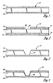
- Figure 1 is an illustration of a conventional conductor/dielectric/conductor organic substrate used in printed circuit and flexible circuit manufacture;
- Figure 2 illustrates a top conductor layer which has been removed by a photoresist process;
- Figure 3 illustrates a laser defined "well";
- Figure 4 illustrates an electroless and electrolytic conductor deposit over ' the substrate and into the side walls and base of the "well";
- Figure 5 illustrates the base substrate with additional conductor layers deposited in the well;
- Figure 6 illustrates how a dielectric layer and a conductor "cap" layer may be laminated onto the substrate to form a second layer of circuitry;
- Figure 7 illustrates a via which is formed to interconnect circuit layers of the base substrate;
- Figure 8 illustrates the base substrate after the bottom conductive layer has been etched;
- Figure 9 depicts the base substrate after the dielectric material has been removed;
- Figure 10 illustrates a finished two layer substrate with raised metallic contacts having a composite conductor metallurgy; and
- Figures 11-16 illustrate alternative process steps of the present invention, wherein the base substrate with raised metallic contacts is laminated to and electrically connected to a multilayer circuit board.
-
- Referring now to the drawings, wherein similar reference characters designate corresponding parts throughout the several views, Figures 1-16 illustrate a process for forming raised metallic contacts, or bumps, on electrical circuits. As may be appreciated by one skilled in the art, although Figures 1-16 depict a process for forming raised metallic contacts on a two layer electrical circuit, any number of circuit layers may be formed utilizing the teachings of the present invention.
- As best illustrated by Figure 1, a
base substrate 10 is provided which is defined by a laminate comprised of a conductive layer 12 (such as copper, for example), adielectric layer 14, and a conductive layer 16 (such as copper, for example). Thedielectric layer 14 must not comprise a material which is resistant to etching by a laser or plasma process, such as a glass reinforced dielectric layer or a dielectric layer reinforced with ceramic particles. Suitable dielectric materials include, but are not limited to polyimides and polyimide laminates, epoxy resins, organic materials, or dielectric materials comprised at least in part of polytetrafluoroethylene. A preferred dielectric material may be obtained from W.L. Gore & Associates, Inc. under the tradename SPEEDBOARD™ dielectric materials. - The thickness of the
dielectric layer 14 is important. This thickness will define the height of the resulting raised metallic contacts which are formed by the teachings herein. Additional detail on the significance ofdielectric layer 14 will be described below. -
Photoresist 18 is applied tocopper layers copper layer 12 where the raised metallic contacts are to be formed. The copper in an exposedarea 20 is etched away by any suitable conventional copper etchant, such as a cupric chloride based etchant solution. Figure 2 illustrates thebase substrate 10 after the copper within the exposedarea 20 has been etched away. An exposedportion 22 ofdielectric layer 14 is shown. Thephotoresist 18 may then be removed from the substrate. - The exposed
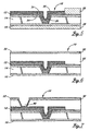
dielectric portion 22 is ablated away with a laser to define a "well" 24 into which a metallic contact will be formed, as shown in Figure 3. As should be understood, thecopper layer 12 functions as a mask to permit ablation of the exposeddielectric portion 22. Thecopper layer 16 acts as a stop and will define the bottom of the well 24. - The ablation of the exposed
dielectric portion 22 may be accomplished by any laser suitable for selective ablation of organic dielectrics, without removing a copper layer. Lasers which operate in ultra violet wavelengths are particularly well suited, such as excimer lasers, and frequency tripled or quadrupled YAG lasers. However, other types of lasers are also suitable. The laser may be operated either in a scanning mode, in which the surface of the substrate is swept with a large laser spot, or in a focused beam. In addition to laser ablation of the exposeddielectric portion 22, other processes may be employed to selectively remove the exposeddielectric portion 22, such as but not limited to plasma etching, reactive ion etching, or chemical etching. However, a laser ablation process is particularly well suited, as it permits more control over the shape of the well 24. Simple diffraction will provide a tapered conical shape in the case of scanning mode laser ablation process. - After the well 24 has been defined, the
base substrate 10 is processed in any suitable manner which deposits a surfaceconductive layer 26, such as copper, on the side walls of the well 24. Suitable processes include, but are not limited to a conventional electroless copper plating operation, sputtering, evaporation, or deposition of a conductive coating which allows direct electrodeposition, or any other suitable process. Additional electrolytically deposited copper may be added to thicken this deposit, thereby providing a more robust surface for additional process steps. Figure 4 illustrates thebase substrate 10 after this conductive deposition step. - The
base substrate 10 is then coated withphotoresist 28 on both sides of the base substrate, and the photoresist is processed to define patterns onconductive layer 12, into which additional metal is deposited to simultaneously form at least one metal "bump" contacts and traces for an electric circuit. - In one embodiment of the present invention, a sacrificial layer of
nickel 30 is first deposited to act as a diffusion barrier during subsequent lamination operations. A layer ofgold 31, which will ultimately form the top layer of the bump contact is then deposited. Thereafter, and a second layer ofnickel 34 is deposited to form a diffusion barrier. A layer ofcopper 36, which will comprise the bulk of the metal, is then deposited. Figure 5 illustrates a substrate with the metals deposited as described. - After deposition is complete, the
photoresist 28 is removed from thebase substrate 10. Thebase substrate 10 may then be treated in a conventional oxide process, such as is common in the production of printed circuits. The rough oxide formed on the surface of the exposed copper of the base substrate will serve to provide adequate adhesion of the metal to a dielectric material in subsequent lamination processes. - As best seen by reference to Figure 6, in one embodiment of the present invention a layer of a
dielectric prepreg material 33, and a "cap" layer ofcopper 32 may be laminated onto thebase substrate 10. The temperature, pressure, and time required for the lamination process should be as specified by the manufacturer of the particular dielectric prepreg used. Thiscopper layer 32 will form the base for a second metal layer of the electric circuit. The dielectric prepreg material may be similar to that used to form thedielectric layer 14. During this lamination process, resin from thedielectric prepreg material 33 will flow into and fill the void space remaining in thewell 24. - Figure 7 illustrates a via 40 which is formed to interconnect the top
conductive layer 32 to theconductive layer 12. Via 40 is formed using the same process as described for the formation of the well 24, except that the deposition of the contact and diffusion barrier metals are not necessary. - As best illustrated in Figure 8, the top metal layer of the base substrate is then coated with
photoresist 42.Conductive layer 16 is then etched away using a suitable etchant. Figure 8 illustratesbase substrate 10 after the bottomconductive layer 16 has been etched. Thephotoresist 42 is then removed fromconductive layer 16. - After the
conductive layer 16 has been etched away, the now exposeddielectric material 14 is removed by any suitable process which will selectively remove dielectric from a conductor such as copper. Suitable processes include but are not limited to plasma etching, laser ablation, reactive ion etching, or chemical etching. Care must be taken that all of thedielectric material 14 is removed from theconductive layer 12, as any remainingdielectric material 14 will prevent theconductive layer 12 from being etched away in subsequent process steps. Figure 9 depicts thebase substrate 10 after thedielectric material 14 has been removed. - The top layer of the
base substrate 10 is then coated with photoresist to protect it from the etchant which is used to remove the exposedconductive layer 12 and surfaceconductive layer 26. Any suitable etchant may be employed. It may be desirable to employ an etchant that will not only remove theconductive layers sacrificial nickel layer 30, such as cupric chloride, for example. However, the cupric chloride etchant will not etch the gold beneath the nickel, thus, and in this embodiment of the present invention, a copper/nickel/gold metallurgy remains to form the metallurgy for abump 50, as well as the metallurgy of the interconnecting traces. The photoresist may then be removed from the circuit. Figure 10 illustrates a finished circuit made in accordance with the teachings of one embodiment of the present invention. - As best seen with reference to Figures 1-10, the height of the
bump 50 is determined by the thickness of thedielectric layer 14, minus the sum of the thickness of thecopper layer 12, the surfaceconductive copper layer 24, and the diffusion barrier ofnickel 30. As the variousconductive layers dielectric layer 14. To maintain consistent height of the bumps across a large panel, one need only control the thickness of thedielectric layer 14. It is common that dielectrics available today offer thickness control of +/-10% or better, thus the planarity of the bumps created will approach +/-10%. The ability to control the bump height by controlling the thickness of thedielectric layer 14, and the degree of planarity achievable by this method is a significant improvement over the method of etching depressions in a mandrel, as described in U.S. Patent 5,197,184. - As best seen with reference to Figures 11-16, in an alternative embodiment of the present invention, process steps are described which permit a
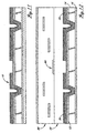
base substrate 10, with raisedmetallic contacts 50, to be laminated and electrically connected to a multilayer circuit board. - Turning to Figure 11, the
base substrate 10 is shown as made by the process steps which are described referencing Figures 1-5. Thebase substrate 10 is laminated to amultilayer circuit board 80 with a dielectric prepreg material, as best seen by reference to Figure 12. The temperature, pressure, and time required for the lamination process should be as specified by the manufacturer of the particular dielectric prepreg used. - The multilayer circuit board may have any number of configurations. However, the side which is to be laminated to the
base substrate 10 must have a series ofpads 60 arranged such thatvias 40 may later connect these pads to thebase substrate 10, as best seen by sequentially viewing Figures 12-16. The opposite side of the multilayer circuit board may be finished prior to lamination, or may have only an unfinished copper layer, in which case this layer will be finished at the same time as the side with the raised contacts. - The top metal layer of the
multi-layer circuit board 80 is then coated with photoresist to protect it from an etchant which is used to etch theconductive layer 16 from thebase substrate 10. Any suitable etchant may be used. The photoresist is then removed from themulti-layer circuit board 80. - After the
conductive layer 16 has been etched away, the now exposeddielectric material 14 is removed by any suitable process for removing a dielectric material from a conductor, such as copper, to thereby expose the raisedmetallic contacts 50, as best seen in Figure 13. Such a suitable process may include, but is not limited to a plasma etching process, laser ablation, reactive ion etching, or chemical etching, for example. Care must be taken to remove all of the dielectric material from the conductive surface, as any remaining dielectric material will prevent the conductive material from being etched in subsequent process steps. - The top layer of the
multi-layer circuit board 80 is then coated with photoresist to protect it from the etchant which is used to remove the exposedconductive layer 12. Any suitable etchant may be employed. It may be desirable to employ an etchant that will not only remove theconductive layer 12, but also thesacrificial nickel layer 30, such as cupric chloride, for example. However, the cupric chloride etchant will not etch the gold beneath the nickel, thus, and in this embodiment of the present invention, a copper/nickel/gold metallurgy remains to form the metallurgy for abump 50, as well as the metallurgy of the interconnecting traces. The photoresist may then be removed from the circuit. Figure 13 illustrates a finished circuit made in accordance with the teachings of the present invention. -
Vias 40 are then drilled in thebase substrate 10 for circuit interconnection. These vias may be either blind or through vias. Thebase substrate 10 is then processed in a conventional electroless copper plating operation such as is common in printed and flexible circuit manufacturing operations. The electroless copper deposits a layer of copper on thebase substrate 10 and on the surface of the side walls of the vias. Additional electrolytically deposited copper may be added to thicken the deposit, and provide a more robust surface for additional process steps. Figure 14 illustrates thebase substrate 10 after such copper deposition. As may be appreciated by one skilled in the art, any suitable process which deposits a conductor may be used in place of the electroless copper process, such as but not limited to sputtering, evaporation, or deposition of a conductive coating which allows direct electrodeposition. - The base substrate is then coated with
photoresist 28 on both sides, and the photoresist is processed to define patterns into which additional metal is deposited to form via and pad connections. Additional copper would likely be deposited. Also, a final etch resistant metal such as nickel, gold or solder may then be deposited. Figure 15 illustrates a base substrate with the metals deposited as described hereinabove. After deposition is complete, thephotoresist 28 is removed from the base substrate. - The
base substrate 10 is then etched in a suitable copper etchant to remove the copper from the areas which were previously covered with photoresist. The circuit may then be routed from a panel. A completed substrate is shown in Figure 16. - Although a few exemplary embodiments of the present invention have been described in detail above, those skilled in the art readily appreciate that many modifications are possible without materially departing from the novel teachings and advantages which are described herein. Accordingly, all such modifications are intended to be included within the scope of the present invention, as defined by the following claims.
Claims (6)
- A method of forming at least one raised metallic contact on an electrical circuit, said method comprising the following steps:providing a composite base substrate which is defined by at least a first conductive layer, a dielectric material and a second conductive layer;removing a predetermined portion of the first conductive layer to expose the dielectric material;removing said exposed portion of the dielectric material up to the second conductive layer, thereby forming a depression;depositing at least one layer of conductive material on at least side wall portions of said depression;removing said second conductive layer; andremoving said dielectric material thereby forming a raised metallic contact which extends perpendicularly away from said first conductive layer.
- A method of forming at least one raised metallic contact on an electrical circuit, said method comprising the following steps:providing a composite base substrate having opposed planar surfaces, the composite base substrate being defined by at least a first conductive layer, a first dielectric material and a second conductive layer;removing a predetermined portion of the first conductive layer to expose the dielectric material;removing said exposed portion of the dielectric material up to the second conductive layer thereby forming a depression;depositing at least one layer of conductive material on at least side wall portions of said depression;laminating at least a second dielectric material to the first planar surface of said composite base substrate;removing said second conductive layer; andremoving said first dielectric material thereby forming a raised metallic contact which extends perpendicularly away from said first conductive layer.
- The method of claim 2 further including the step of depositing a third conductive layer on said second dielectric material.
- The method of claim 3 further including the steps of:removing a predetermined portion of the third conductive layer to expose a portion of said second dielectric material;removing said exposed portion of said second dielectric material up to said first conductive layer, thereby forming a depression; andelectrically connecting said third conductive layer to said first conductive layer.
- A method of forming at least one raised metallic contact on an electrical circuit, said method comprising the following steps:providing a composite base substrate which is defined by at least a first copper layer, a dielectric material and a second copper layer;removing a predetermined portion of the first copper layer to expose the dielectric material;removing said exposed dielectric material up to said second copper layer, thereby forming a depression;depositing at least a third copper layer on at least side wall portions of said depression;depositing at least one conductive layer on said third copper layer, wherein said conductive layer is not copper;removing said second copper layer, andremoving said dielectric material thereby forming a raised metallic contact which extends perpendicularly away from said first conductive layer.
- The method of claims 1, 2, or 5 further including the step of laminating the base substrate to a printed circuit board.
Applications Claiming Priority (3)
| Application Number | Priority Date | Filing Date | Title |
|---|---|---|---|
| US08/655,017 US5747358A (en) | 1996-05-29 | 1996-05-29 | Method of forming raised metallic contacts on electrical circuits |
| US655017 | 1996-05-29 | ||
| PCT/US1997/008011 WO1997046061A1 (en) | 1996-05-29 | 1997-05-08 | Method of forming raised metallic contacts on electrical circuits |
Publications (2)
| Publication Number | Publication Date |
|---|---|
| EP0843955A1 EP0843955A1 (en) | 1998-05-27 |
| EP0843955B1 true EP0843955B1 (en) | 2004-03-24 |
Family
ID=24627163
Family Applications (1)
| Application Number | Title | Priority Date | Filing Date |
|---|---|---|---|
| EP97923639A Expired - Lifetime EP0843955B1 (en) | 1996-05-29 | 1997-05-08 | Method of forming raised metallic contacts on electrical circuits |
Country Status (7)
| Country | Link |
|---|---|
| US (2) | US5747358A (en) |
| EP (1) | EP0843955B1 (en) |
| JP (1) | JP3759754B2 (en) |
| KR (2) | KR100304317B1 (en) |
| AU (1) | AU2940097A (en) |
| DE (1) | DE69728234T2 (en) |
| WO (1) | WO1997046061A1 (en) |
Families Citing this family (61)
| Publication number | Priority date | Publication date | Assignee | Title |
|---|---|---|---|---|
| US7579269B2 (en) * | 1993-11-16 | 2009-08-25 | Formfactor, Inc. | Microelectronic spring contact elements |
| US6727580B1 (en) | 1993-11-16 | 2004-04-27 | Formfactor, Inc. | Microelectronic spring contact elements |
| US6482013B2 (en) | 1993-11-16 | 2002-11-19 | Formfactor, Inc. | Microelectronic spring contact element and electronic component having a plurality of spring contact elements |
| US7073254B2 (en) | 1993-11-16 | 2006-07-11 | Formfactor, Inc. | Method for mounting a plurality of spring contact elements |
| US8033838B2 (en) | 1996-02-21 | 2011-10-11 | Formfactor, Inc. | Microelectronic contact structure |
| US5918153A (en) * | 1996-09-18 | 1999-06-29 | Sandia Corporation | High density electronic circuit and process for making |
| US6809421B1 (en) | 1996-12-02 | 2004-10-26 | Kabushiki Kaisha Toshiba | Multichip semiconductor device, chip therefor and method of formation thereof |
| US6520778B1 (en) | 1997-02-18 | 2003-02-18 | Formfactor, Inc. | Microelectronic contact structures, and methods of making same |
| US6246548B1 (en) | 1997-03-24 | 2001-06-12 | Maxtor Corporation | Mechanically formed standoffs in a circuit interconnect |
| US6040239A (en) * | 1997-08-22 | 2000-03-21 | Micron Technology, Inc. | Non-oxidizing touch contact interconnect for semiconductor test systems and method of fabrication |
| JP3080047B2 (en) * | 1997-11-07 | 2000-08-21 | 日本電気株式会社 | Bump structure and bump structure forming method |
| US6807734B2 (en) * | 1998-02-13 | 2004-10-26 | Formfactor, Inc. | Microelectronic contact structures, and methods of making same |
| JP3553791B2 (en) * | 1998-04-03 | 2004-08-11 | 株式会社ルネサステクノロジ | CONNECTION DEVICE AND ITS MANUFACTURING METHOD, INSPECTION DEVICE, AND SEMICONDUCTOR ELEMENT MANUFACTURING METHOD |
| US6299456B1 (en) * | 1998-04-10 | 2001-10-09 | Micron Technology, Inc. | Interposer with contact structures for electrical testing |
| US6278185B1 (en) * | 1998-05-27 | 2001-08-21 | Intel Corporation | Semi-additive process (SAP) architecture for organic leadless grid array packages |
| US6998711B1 (en) * | 1998-08-14 | 2006-02-14 | Micron Technology, Inc. | Method of forming a micro solder ball for use in C4 bonding process |
| US6136689A (en) * | 1998-08-14 | 2000-10-24 | Micron Technology, Inc. | Method of forming a micro solder ball for use in C4 bonding process |
| US6491968B1 (en) | 1998-12-02 | 2002-12-10 | Formfactor, Inc. | Methods for making spring interconnect structures |
| US6672875B1 (en) | 1998-12-02 | 2004-01-06 | Formfactor, Inc. | Spring interconnect structures |
| KR20080047629A (en) * | 1998-12-02 | 2008-05-29 | 폼팩터, 인크. | Method of making an electrical contact structure |
| US6255126B1 (en) * | 1998-12-02 | 2001-07-03 | Formfactor, Inc. | Lithographic contact elements |
| US6268015B1 (en) | 1998-12-02 | 2001-07-31 | Formfactor | Method of making and using lithographic contact springs |
| US6181569B1 (en) * | 1999-06-07 | 2001-01-30 | Kishore K. Chakravorty | Low cost chip size package and method of fabricating the same |
| US6569604B1 (en) * | 1999-06-30 | 2003-05-27 | International Business Machines Corporation | Blind via formation in a photoimageable dielectric material |
| JP2001053438A (en) * | 1999-08-16 | 2001-02-23 | Sony Corp | Method for manufacturing multi-layer printed wiring board |
| DE10007414B4 (en) * | 2000-02-18 | 2006-07-06 | eupec Europäische Gesellschaft für Leistungshalbleiter mbH & Co. KG | Process for the through-plating of a substrate for power semiconductor modules by solder and substrate produced by the method |
| US6548224B1 (en) * | 2000-03-07 | 2003-04-15 | Kulicke & Soffa Holdings, Inc. | Wiring substrate features having controlled sidewall profiles |
| US6878396B2 (en) * | 2000-04-10 | 2005-04-12 | Micron Technology, Inc. | Micro C-4 semiconductor die and method for depositing connection sites thereon |
| JP2002026515A (en) * | 2000-07-07 | 2002-01-25 | Toshiba Corp | Printed wiring board and its manufacturing method |
| US6498381B2 (en) * | 2001-02-22 | 2002-12-24 | Tru-Si Technologies, Inc. | Semiconductor structures having multiple conductive layers in an opening, and methods for fabricating same |
| US6574863B2 (en) * | 2001-04-20 | 2003-06-10 | Phoenix Precision Technology Corporation | Thin core substrate for fabricating a build-up circuit board |
| KR20020087328A (en) * | 2001-05-15 | 2002-11-22 | 조수제 | The fabrication of mandrel for electroforming |
| JP2003023067A (en) * | 2001-07-09 | 2003-01-24 | Tokyo Electron Ltd | Formation method for via metal layer and via metal layer formed substrate |
| US6759311B2 (en) | 2001-10-31 | 2004-07-06 | Formfactor, Inc. | Fan out of interconnect elements attached to semiconductor wafer |
| US6599778B2 (en) * | 2001-12-19 | 2003-07-29 | International Business Machines Corporation | Chip and wafer integration process using vertical connections |
| TW583395B (en) * | 2002-03-13 | 2004-04-11 | Scs Hightech Inc | Method for producing micro probe tips |
| US20050142739A1 (en) * | 2002-05-07 | 2005-06-30 | Microfabrica Inc. | Probe arrays and method for making |
| US20060234042A1 (en) * | 2002-09-05 | 2006-10-19 | Rui Yang | Etched dielectric film in microfluidic devices |
| US20040258885A1 (en) * | 2002-09-05 | 2004-12-23 | Kreutter Nathan P. | Etched dielectric film in microfluidic devices |
| US10416192B2 (en) | 2003-02-04 | 2019-09-17 | Microfabrica Inc. | Cantilever microprobes for contacting electronic components |
| US8328564B2 (en) * | 2003-06-13 | 2012-12-11 | Molex Incoporated | Electrical connector solder terminal |
| JP3990347B2 (en) * | 2003-12-04 | 2007-10-10 | ローム株式会社 | Semiconductor chip, manufacturing method thereof, and semiconductor device |
| WO2005067355A2 (en) * | 2003-12-30 | 2005-07-21 | 3M Innovative Properties Company | Patterned circuits and method for making same |
| US7012017B2 (en) * | 2004-01-29 | 2006-03-14 | 3M Innovative Properties Company | Partially etched dielectric film with conductive features |
| JP2006119024A (en) * | 2004-10-22 | 2006-05-11 | Tokyo Electron Ltd | Probe and its manufacturing method |
| JP4619223B2 (en) * | 2004-12-16 | 2011-01-26 | 新光電気工業株式会社 | Semiconductor package and manufacturing method thereof |
| WO2006080073A1 (en) * | 2005-01-27 | 2006-08-03 | Matsushita Electric Industrial Co., Ltd. | Multi-layer circuit substrate manufacturing method and multi-layer circuit substrate |
| US20070023387A1 (en) * | 2005-07-28 | 2007-02-01 | Litton Systems, Inc. | Printed circuit board interconnection and method |
| US7795137B2 (en) * | 2005-08-26 | 2010-09-14 | Hitachi, Ltd. | Manufacturing method of semiconductor device |
| KR100796206B1 (en) * | 2007-02-12 | 2008-01-24 | 주식회사 유니테스트 | Method for manufacturing bump of probe card |
| TWI420607B (en) * | 2007-05-09 | 2013-12-21 | Method of manufacturing electrical contact device | |
| WO2009023284A2 (en) | 2007-08-15 | 2009-02-19 | Tessera, Inc. | Interconnection element with plated posts formed on mandrel |
| US8276269B2 (en) | 2008-06-20 | 2012-10-02 | Intel Corporation | Dual epoxy dielectric and photosensitive solder mask coatings, and processes of making same |
| TWI411368B (en) * | 2009-12-22 | 2013-10-01 | Unimicron Technology Corp | Method for fabricating wiring structure of wiring board |
| DE102013203799A1 (en) * | 2013-03-06 | 2014-09-11 | Robert Bosch Gmbh | Battery cell housing with integrated electronics |
| US9105288B1 (en) * | 2014-03-11 | 2015-08-11 | Magnecomp Corporation | Formed electrical contact pad for use in a dual stage actuated suspension |
| US10448517B2 (en) * | 2016-11-04 | 2019-10-15 | Jabil Inc. | Method and apparatus for flexible circuit cable attachment |
| US11018024B2 (en) * | 2018-08-02 | 2021-05-25 | Nxp Usa, Inc. | Method of fabricating embedded traces |
| US11262383B1 (en) | 2018-09-26 | 2022-03-01 | Microfabrica Inc. | Probes having improved mechanical and/or electrical properties for making contact between electronic circuit elements and methods for making |
| KR20230074582A (en) * | 2020-10-02 | 2023-05-30 | 셀링크 코포레이션 | Forming Connections to Flexible Interconnect Circuits |
| US11876312B2 (en) | 2020-10-02 | 2024-01-16 | Cellink Corporation | Methods and systems for terminal-free circuit connectors and flexible multilayered interconnect circuits |
Family Cites Families (12)
| Publication number | Priority date | Publication date | Assignee | Title |
|---|---|---|---|---|
| US3319317A (en) * | 1963-12-23 | 1967-05-16 | Ibm | Method of making a multilayered laminated circuit board |
| US4125310A (en) * | 1975-12-01 | 1978-11-14 | Hughes Aircraft Co | Electrical connector assembly utilizing wafers for connecting electrical cables |
| US4453795A (en) * | 1975-12-01 | 1984-06-12 | Hughes Aircraft Company | Cable-to-cable/component electrical pressure wafer connector assembly |
| US4116517A (en) * | 1976-04-15 | 1978-09-26 | International Telephone And Telegraph Corporation | Flexible printed circuit and electrical connection therefor |
| US4717066A (en) * | 1986-02-24 | 1988-01-05 | American Telephone And Telegraph Company, At&T Bell Laboratories | Method of bonding conductors to semiconductor devices |
| US4764485A (en) * | 1987-01-05 | 1988-08-16 | General Electric Company | Method for producing via holes in polymer dielectrics |
| US4963225A (en) * | 1989-10-20 | 1990-10-16 | Tektronix, Inc. | Method of fabricating a contact device |
| US5197184A (en) * | 1990-09-11 | 1993-03-30 | Hughes Aircraft Company | Method of forming three-dimensional circuitry |
| US5072520A (en) * | 1990-10-23 | 1991-12-17 | Rogers Corporation | Method of manufacturing an interconnect device having coplanar contact bumps |
| US5211577A (en) * | 1992-10-06 | 1993-05-18 | Hughes Aircraft Company | Pressure-actuated gold dot connector |
| US5326412A (en) * | 1992-12-22 | 1994-07-05 | Hughes Aircraft Company | Method for electrodepositing corrosion barrier on isolated circuitry |
| US5492863A (en) * | 1994-10-19 | 1996-02-20 | Motorola, Inc. | Method for forming conductive bumps on a semiconductor device |
-
1996
- 1996-05-29 US US08/655,017 patent/US5747358A/en not_active Expired - Lifetime
- 1996-11-08 US US08/744,842 patent/US5786270A/en not_active Expired - Lifetime
-
1997
- 1997-05-08 KR KR1019980700518A patent/KR100304317B1/en not_active IP Right Cessation
- 1997-05-08 AU AU29400/97A patent/AU2940097A/en not_active Abandoned
- 1997-05-08 WO PCT/US1997/008011 patent/WO1997046061A1/en active IP Right Grant
- 1997-05-08 EP EP97923639A patent/EP0843955B1/en not_active Expired - Lifetime
- 1997-05-08 KR KR1019980700519A patent/KR100279036B1/en not_active IP Right Cessation
- 1997-05-08 JP JP54247797A patent/JP3759754B2/en not_active Expired - Lifetime
- 1997-05-08 DE DE69728234T patent/DE69728234T2/en not_active Expired - Lifetime
Also Published As
| Publication number | Publication date |
|---|---|
| KR100304317B1 (en) | 2001-11-02 |
| DE69728234T2 (en) | 2005-03-10 |
| DE69728234D1 (en) | 2004-04-29 |
| WO1997046061A1 (en) | 1997-12-04 |
| KR19990035857A (en) | 1999-05-25 |
| KR100279036B1 (en) | 2001-02-01 |
| AU2940097A (en) | 1998-01-05 |
| US5786270A (en) | 1998-07-28 |
| KR19990035858A (en) | 1999-05-25 |
| EP0843955A1 (en) | 1998-05-27 |
| JP3759754B2 (en) | 2006-03-29 |
| US5747358A (en) | 1998-05-05 |
| JPH11509990A (en) | 1999-08-31 |
Similar Documents
| Publication | Publication Date | Title |
|---|---|---|
| EP0843955B1 (en) | Method of forming raised metallic contacts on electrical circuits | |
| US5369881A (en) | Method of forming circuit wiring pattern | |
| US4606787A (en) | Method and apparatus for manufacturing multi layer printed circuit boards | |
| US5774340A (en) | Planar redistribution structure and printed wiring device | |
| EP0469308B1 (en) | Multilayered circuit board assembly and method of making same | |
| EP0476868B1 (en) | Three-dimensional electroformed circuitry | |
| US4591411A (en) | Method for forming a high density printed wiring board | |
| US4663497A (en) | High density printed wiring board | |
| EP0213805A1 (en) | Multilayer circuit board | |
| US6820330B1 (en) | Method for forming a multi-layer circuit assembly | |
| EP0545328A2 (en) | Printed circuit board manufacturing process | |
| US20010050183A1 (en) | Fine pitch circuitization with filled plated through holes | |
| US5364277A (en) | Three-dimensional electroformed circuitry | |
| EP0450381A2 (en) | Multilayer interconnection structure | |
| US4769309A (en) | Printed circuit boards and method for manufacturing printed circuit boards | |
| JPH04282843A (en) | Interconnection device and manufacture thereof | |
| US4912020A (en) | Printed circuit boards and method for manufacturing printed circuit boards | |
| CA1222574A (en) | Method and apparatus for manufacturing multi layer printed circuit boards | |
| US4789423A (en) | Method for manufacturing multi-layer printed circuit boards | |
| US7080448B2 (en) | PCB with inlaid outer-layer circuits and production methods thereof | |
| EP0949855B1 (en) | Process for producing a multilayer circuit board having an electroplated blind hole | |
| EP0426665B1 (en) | Method for manufacturing printed circuit boards | |
| US4847446A (en) | Printed circuit boards and method for manufacturing printed circuit boards | |
| EP0857403B1 (en) | Method of forming raised metallic contacts on electrical circuits for permanent bonding | |
| EP0108116B1 (en) | High density printed wiring board |
Legal Events
| Date | Code | Title | Description |
|---|---|---|---|
| PUAI | Public reference made under article 153(3) epc to a published international application that has entered the european phase |
Free format text: ORIGINAL CODE: 0009012 |
|
| 17P | Request for examination filed |
Effective date: 19971204 |
|
| AK | Designated contracting states |
Kind code of ref document: A1 Designated state(s): DE FR GB NL |
|
| GRAP | Despatch of communication of intention to grant a patent |
Free format text: ORIGINAL CODE: EPIDOSNIGR1 |
|
| GRAS | Grant fee paid |
Free format text: ORIGINAL CODE: EPIDOSNIGR3 |
|
| GRAA | (expected) grant |
Free format text: ORIGINAL CODE: 0009210 |
|
| AK | Designated contracting states |
Kind code of ref document: B1 Designated state(s): DE FR GB NL |
|
| REG | Reference to a national code |
Ref country code: GB Ref legal event code: FG4D |
|
| REF | Corresponds to: |
Ref document number: 69728234 Country of ref document: DE Date of ref document: 20040429 Kind code of ref document: P |
|
| ET | Fr: translation filed | ||
| PLBE | No opposition filed within time limit |
Free format text: ORIGINAL CODE: 0009261 |
|
| STAA | Information on the status of an ep patent application or granted ep patent |
Free format text: STATUS: NO OPPOSITION FILED WITHIN TIME LIMIT |
|
| 26N | No opposition filed |
Effective date: 20041228 |
|
| REG | Reference to a national code |
Ref country code: FR Ref legal event code: PLFP Year of fee payment: 20 |
|
| PGFP | Annual fee paid to national office [announced via postgrant information from national office to epo] |
Ref country code: NL Payment date: 20160422 Year of fee payment: 20 |
|
| PGFP | Annual fee paid to national office [announced via postgrant information from national office to epo] |
Ref country code: DE Payment date: 20160421 Year of fee payment: 20 Ref country code: GB Payment date: 20160426 Year of fee payment: 20 |
|
| PGFP | Annual fee paid to national office [announced via postgrant information from national office to epo] |
Ref country code: FR Payment date: 20160422 Year of fee payment: 20 |
|
| REG | Reference to a national code |
Ref country code: DE Ref legal event code: R071 Ref document number: 69728234 Country of ref document: DE |
|
| REG | Reference to a national code |
Ref country code: NL Ref legal event code: MK Effective date: 20170507 |
|
| REG | Reference to a national code |
Ref country code: GB Ref legal event code: PE20 Expiry date: 20170507 |
|
| PG25 | Lapsed in a contracting state [announced via postgrant information from national office to epo] |
Ref country code: GB Free format text: LAPSE BECAUSE OF EXPIRATION OF PROTECTION Effective date: 20170507 |