EP0843323B1 - Current leads adapted for use with superconducting coil and formed of functionally gradient material - Google Patents
Current leads adapted for use with superconducting coil and formed of functionally gradient material Download PDFInfo
- Publication number
- EP0843323B1 EP0843323B1 EP97119503A EP97119503A EP0843323B1 EP 0843323 B1 EP0843323 B1 EP 0843323B1 EP 97119503 A EP97119503 A EP 97119503A EP 97119503 A EP97119503 A EP 97119503A EP 0843323 B1 EP0843323 B1 EP 0843323B1
- Authority
- EP
- European Patent Office
- Prior art keywords
- temperature
- current
- current lead
- room
- thermoelectric semiconductor
- Prior art date
- Legal status (The legal status is an assumption and is not a legal conclusion. Google has not performed a legal analysis and makes no representation as to the accuracy of the status listed.)
- Expired - Lifetime
Links
- 239000000463 material Substances 0.000 title claims description 37
- 239000004065 semiconductor Substances 0.000 claims description 51
- 239000002887 superconductor Substances 0.000 claims description 30
- IJGRMHOSHXDMSA-UHFFFAOYSA-N Atomic nitrogen Chemical compound N#N IJGRMHOSHXDMSA-UHFFFAOYSA-N 0.000 claims description 13
- 229910016312 BiSb Inorganic materials 0.000 claims description 10
- 239000007788 liquid Substances 0.000 claims description 8
- 229910052757 nitrogen Inorganic materials 0.000 claims description 6
- 229910015901 Bi-Sr-Ca-Cu-O Inorganic materials 0.000 claims description 4
- 229910002899 Bi2Te3 Inorganic materials 0.000 claims description 3
- 239000004020 conductor Substances 0.000 description 11
- 239000001307 helium Substances 0.000 description 5
- 229910052734 helium Inorganic materials 0.000 description 5
- SWQJXJOGLNCZEY-UHFFFAOYSA-N helium atom Chemical compound [He] SWQJXJOGLNCZEY-UHFFFAOYSA-N 0.000 description 5
- 230000005679 Peltier effect Effects 0.000 description 4
- 238000001816 cooling Methods 0.000 description 4
- 239000010949 copper Substances 0.000 description 4
- 230000000694 effects Effects 0.000 description 4
- 229910052802 copper Inorganic materials 0.000 description 3
- 239000007789 gas Substances 0.000 description 3
- RYGMFSIKBFXOCR-UHFFFAOYSA-N Copper Chemical compound [Cu] RYGMFSIKBFXOCR-UHFFFAOYSA-N 0.000 description 2
- 239000012535 impurity Substances 0.000 description 2
- KWQLUUQBTAXYCB-UHFFFAOYSA-K antimony(3+);triiodide Chemical compound I[Sb](I)I KWQLUUQBTAXYCB-UHFFFAOYSA-K 0.000 description 1
- 230000004927 fusion Effects 0.000 description 1
- -1 i.e. Substances 0.000 description 1
- 238000012423 maintenance Methods 0.000 description 1
- 229910052751 metal Inorganic materials 0.000 description 1
- 239000002184 metal Substances 0.000 description 1
- 150000002739 metals Chemical class 0.000 description 1
- 238000011160 research Methods 0.000 description 1
- 239000000126 substance Substances 0.000 description 1
Images

Classifications
-
- H—ELECTRICITY
- H01—ELECTRIC ELEMENTS
- H01F—MAGNETS; INDUCTANCES; TRANSFORMERS; SELECTION OF MATERIALS FOR THEIR MAGNETIC PROPERTIES
- H01F6/00—Superconducting magnets; Superconducting coils
- H01F6/06—Coils, e.g. winding, insulating, terminating or casing arrangements therefor
- H01F6/065—Feed-through bushings, terminals and joints
-
- Y—GENERAL TAGGING OF NEW TECHNOLOGICAL DEVELOPMENTS; GENERAL TAGGING OF CROSS-SECTIONAL TECHNOLOGIES SPANNING OVER SEVERAL SECTIONS OF THE IPC; TECHNICAL SUBJECTS COVERED BY FORMER USPC CROSS-REFERENCE ART COLLECTIONS [XRACs] AND DIGESTS
- Y10—TECHNICAL SUBJECTS COVERED BY FORMER USPC
- Y10S—TECHNICAL SUBJECTS COVERED BY FORMER USPC CROSS-REFERENCE ART COLLECTIONS [XRACs] AND DIGESTS
- Y10S257/00—Active solid-state devices, e.g. transistors, solid-state diodes
- Y10S257/93—Thermoelectric, e.g. peltier effect cooling
-
- Y—GENERAL TAGGING OF NEW TECHNOLOGICAL DEVELOPMENTS; GENERAL TAGGING OF CROSS-SECTIONAL TECHNOLOGIES SPANNING OVER SEVERAL SECTIONS OF THE IPC; TECHNICAL SUBJECTS COVERED BY FORMER USPC CROSS-REFERENCE ART COLLECTIONS [XRACs] AND DIGESTS
- Y10—TECHNICAL SUBJECTS COVERED BY FORMER USPC
- Y10S—TECHNICAL SUBJECTS COVERED BY FORMER USPC CROSS-REFERENCE ART COLLECTIONS [XRACs] AND DIGESTS
- Y10S505/00—Superconductor technology: apparatus, material, process
- Y10S505/70—High TC, above 30 k, superconducting device, article, or structured stock
-
- Y—GENERAL TAGGING OF NEW TECHNOLOGICAL DEVELOPMENTS; GENERAL TAGGING OF CROSS-SECTIONAL TECHNOLOGIES SPANNING OVER SEVERAL SECTIONS OF THE IPC; TECHNICAL SUBJECTS COVERED BY FORMER USPC CROSS-REFERENCE ART COLLECTIONS [XRACs] AND DIGESTS
- Y10—TECHNICAL SUBJECTS COVERED BY FORMER USPC
- Y10S—TECHNICAL SUBJECTS COVERED BY FORMER USPC CROSS-REFERENCE ART COLLECTIONS [XRACs] AND DIGESTS
- Y10S505/00—Superconductor technology: apparatus, material, process
- Y10S505/70—High TC, above 30 k, superconducting device, article, or structured stock
- Y10S505/704—Wire, fiber, or cable
-
- Y—GENERAL TAGGING OF NEW TECHNOLOGICAL DEVELOPMENTS; GENERAL TAGGING OF CROSS-SECTIONAL TECHNOLOGIES SPANNING OVER SEVERAL SECTIONS OF THE IPC; TECHNICAL SUBJECTS COVERED BY FORMER USPC CROSS-REFERENCE ART COLLECTIONS [XRACs] AND DIGESTS
- Y10—TECHNICAL SUBJECTS COVERED BY FORMER USPC
- Y10S—TECHNICAL SUBJECTS COVERED BY FORMER USPC CROSS-REFERENCE ART COLLECTIONS [XRACs] AND DIGESTS
- Y10S505/00—Superconductor technology: apparatus, material, process
- Y10S505/70—High TC, above 30 k, superconducting device, article, or structured stock
- Y10S505/706—Contact pads or leads bonded to superconductor
-
- Y—GENERAL TAGGING OF NEW TECHNOLOGICAL DEVELOPMENTS; GENERAL TAGGING OF CROSS-SECTIONAL TECHNOLOGIES SPANNING OVER SEVERAL SECTIONS OF THE IPC; TECHNICAL SUBJECTS COVERED BY FORMER USPC CROSS-REFERENCE ART COLLECTIONS [XRACs] AND DIGESTS
- Y10—TECHNICAL SUBJECTS COVERED BY FORMER USPC
- Y10S—TECHNICAL SUBJECTS COVERED BY FORMER USPC CROSS-REFERENCE ART COLLECTIONS [XRACs] AND DIGESTS
- Y10S505/00—Superconductor technology: apparatus, material, process
- Y10S505/825—Apparatus per se, device per se, or process of making or operating same
- Y10S505/888—Refrigeration
- Y10S505/891—Magnetic or electrical effect cooling
Definitions
- the present invention relates to superconducting-coil current leads which are used to connect a power supply placed in a room-temperature environment to a superconducting coil placed in an ultralow-temperature environment.
- a superconducting coil used for such a purpose is kept at an ultralow temperature of 4K or so, but a power supply for exciting the superconducting coil is kept at room temperature. Therefore, a current lead, which is part of an electric circuit including the power supply and the superconducting coil, includes portions kept at room temperature and portions kept at ultralow temperature. In the current lead, the heat conduction arises from the temperature difference and Joule heat is generated by current flow, and heat travels from the room-temperature portions to the ultralow-temperature portions.
- the amount of heat traveling from the room-temperature portions to the ultralow-temperature portions is larger than a half of the total amount of heat entering the large-sized superconducting coil system.
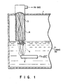
- a gas-cooled current lead such as that shown in FIG. 1, is employed to reduce the amount of heat that enters the system through the current lead.
- the mathematical product between the heat conductivity and the electrical resistance should be as small as possible.
- current leads are formed of normal conductors, i.e., metals such as Cu and Al.
- a superconducting coil covered with a conduit 3 is immersed in the liquid helium 2 contained in a cryostat 1.
- a large number of superconducting strands 4 are led out of the conduit 3 and connected to the respective current lead strands 5.
- the current lead strands 5 are housed inside a current lead tube 6 and led out of the cryostat 1. The use of a large number of current lead strands is useful in increasing the ratio of the surface area to the cross sectional area.
- the liquid helium 2 gasifies due to the heat that enters the system through the current lead strands 5.
- the resultant cold helium gas passes through the current lead tube 6 and exchanges heat with reference to the current lead strands. Then, the helium gas flows out from the upper portion of the current lead tube 6. Since, in this manner, the current lead strands 5 are cooled by the cold helium gas, the heat conduction to a lower temperature region is suppressed.
- FIG. 2 An example of such a current lead as it is known from US-A-5,802,855 is shown in FIG. 2.
- a power supply 100 placed in a room-temperature environment and a superconducting coil 200 placed in an ultralow-temperature environment are connected together by means of a current lead 11, which is obtained by joining a normal conductor 12 and a high-temperature superconductor 13 together.
- a high-temperature superconductor recently developed does not have an electric resistance even at the temperature of a liquid nitrogen (77K) or thereabouts, as long as it is placed in a low magnetic field. This being so, the high-temperature superconductor allows conduction of a large amount of current, and yet it does not generate heat owing to superconduction.
- the heat conductivity which it has at a temperature of 100K to 10K is about 1/1,000 of that of copper. Due to these characteristics, the use of the high-temperature superconductor is effective in suppressing the heat which may enter the system by way of the current lead 11.
- This Peltier current lead is made up of a first current lead 21a and a second current lead 21b, the former being obtained by joining an N-type thermoelectric semiconductor 22a, a normal conductor 23 and a high-temperature superconductor 24 together, and the latter being obtained by joining a P-type thermoelectric semiconductor 22b, a normal conductor 23 and a high-temperature superconductor 24 together.
- the Peltier current lead connects a power supply 100 located in a roomtemperature environment and a superconducting coil 200 located in an ultralow-temperature environment.
- the N- and P-type thermoelectric semiconductors 22a and 22b are formed of a BiTe-based material or a BiTeSb-based material.
- a current from the power supply 100 flows first through the first current lead 21a, then through the superconducting coil 200, then through the second current lead 21b, and then returns to the power supply 100.
- thermoelectric semiconductors 22a and 22b When a current is supplied to the N- and P-type thermoelectric semiconductors 22a and 22b of the current leads 21a and 21b, as indicated by the arrows shown in FIG. 3, the thermoelectric semiconductors 22a and 22b exhibit the Peltier effect and thus function as a heat pump. Thus, heat is conveyed from the low-temperature region to the room-temperature region.
- the thermoelectric semiconductors 22a and 22b are formed of a BiTe-based material or a BiTeSb-based material, they can cool an object to as low as 200K or thereabouts in the state where there is no heat load. As a result, those portions of the current leads 21a and 21b which are located in the room-temperature environment are cooled, and heat is not transmitted to the ultralow-temperature portions of the system.
- the high-temperature superconductor 24 is used at a temperature lower than that of liquid nitrogen. In practice, however, it cannot be cooled to this low temperature if the thermoelectric semiconductors are formed of a BiTe-based or BiTeSb-based material. This is why the normal conductors 23 are inserted between the thermoelectric semiconductors 22a, 22b and the high-temperature superconductors 24. At room temperature or thereabouts, the thermoelectric semiconductors formed of the BiTe-based or BiTeSb-based material has a heat conductivity which is about 1/200 of that of copper. Hence, heat is not transmitted to the ultralow-temperature region even when no current is supplied.
- An object of the present invention is to provide superconducting-coil current leads formed of a functionally gradient material (FGM) that is capable of remarkably reducing the amount of heat transmitted from the room-temperature region to the ultralow-temperature region.
- FGM functionally gradient material
- the superconducting-coil current leads provided by the present invention are formed of a functionally gradient material and used to connect a power source placed in the room-temperature environment and the superconducting coil placed in the ultralow-temperature environment.
- the current leads include a first current lead and a second current lead according to claim 1.
- the first current lead is made up of a room-temperature N-type thermoelectric semiconductor, a low-temperature N-type thermoelectric semiconductor, and a high-temperature superconductor.
- the second current lead is made up of a room-temperature P-type thermoelectric semiconductor, a low-temperature P-type thermoelectric semiconductor, and a high-temperature superconductor.
- At least one of the first and second current leads is formed of a functionally gradient material.
- the first and second leads are connected in such a manner that a current from the power source flows through the first current lead, the superconducting coil and the second current lead in the order mentioned and then returns to the power source.
- low temperature in the term "low-temperature thermoelectric semiconductor” is used herein to represent a temperature which is lower than the room temperature and is higher than the ultralow-temperature, i.e., the operating temperature of the high-temperature superconductor.
- Room-temperature N- and P-type thermoelectric semiconductors (which are adapted for use at room temperature) are formed of either a BiTe-based material or a BiTeSb-based material. Examples of such materials are Bi 2 Te 3 and (BiSb) 2 Te 3 . In the case where thermoelectric semiconductors formed of such materials are used as Peltier elements, a satisfactory cooling effect is attained in the temperature range approximately between the room temperature and 200K.
- thermoelectric semiconductors which are adapted for use at low temperature
- BiSb-based materials are formed of BiSb-based materials.
- thermoelectric semiconductors formed of such materials are used as Peltier elements, a satisfactory cooling effect is attained in the temperature range approximately between 200K and 77K (77K: the temperature of liquid nitrogen).
- thermoelectric semiconductors become “N” in conductivity if impurities such as SbI 3 are doped, and become “P” in conductivity if impurities such as PbI 3 are doped.
- they can be controlled in conductivity type ("N" or "P") by slightly varying the amount of each element with reference to the stoichiometric ratio.
- the room-temperature thermoelectric semiconductor and low-temperature thermoelectric semiconductor may be different in cross section and/or length in accordance with the property have and the characteristics required for them.
- the high-temperature superconductor is formed of a Bi-based material such as Bi-Sr-Ca-Cu-O (Bi-2223, Bi-2212).
- the room-temperature thermoelectric semiconductor is formed of either a BiTe-based material or a BiTeSb-based material
- the low-temperature thermoelectric semiconductor is formed of a BiSb-based material
- the high-temperature superconductor is formed of a Bi-based material.
- FIG. 4 An example of a current lead which the present invention provides as being suitable for use with a superconducting coil is shown in FIG. 4.
- a power supply 100 placed in a room temperature environment and a superconducting coil 200 placed in an ultralow-temperature environment are connected together by means of a first current lead 31a and a second current lead 31b.
- the first current lead 31a is made up of a room-temperature N-type thermoelectric semiconductor 32a formed of a BiTe- or BiTeSb-based material, a low-temperature N-type thermoelectric semiconductor 33a formed of a BiSb-based material, and a high-temperature superconductor 34 formed of a Bi-based material. These elements of the first current lead 31a are jointed together.
- the second current lead 31b is made up of a room-temperature P-type thermoelectric semiconductor 32b formed of a BiTe- or BiTeSb-based material, a low-temperature P-type thermoelectric semiconductor 33b formed of a BiSb-based material, and a high-temperature superconductor 34 formed of a Bi-based material. These elements of the second current lead 31b are jointed together.
- a current from the power supply 100 flows first through the first current lead 31a, then through the superconducting coil 200, then through the second current lead 31b, and then returns to the power supply 100.
- thermoelectric semiconductors 32a and 32b function as a heat pump, and heat is transmitted from the low-temperature region to the room-temperature region. Since the thermoelectric semiconductors are formed of a BiTe-based material or BiTeSb-based material, they can cool an object to as low as 200K or thereabouts in the state where there is no heat load.
- thermoelectric semiconductors 33a and 33b also function as a heat pump, and heat is transmitted from the low-temperature region to the room-temperature region. Since the thermoelectric semiconductors 33a and 33b are formed of a BiSb-based material, they can cool an object from 200K to 77K (i.e., the temperature of liquid nitrogen) in the state where there is no heat load.
- the current leads 31a and 31b which are located in the room-temperature region decrease in temperature, thus suppressing the heat which may be transmitted to the low-temperature region.
- the current leads of the present invention do not comprise a normal conductor having a high heat conductivity. Therefore, the present invention provides a solution to the problem of the prior art, wherein the heat transmitted through a normal conductor enters the system.
- the heat conductivity of each thermoelectric semiconductor is about 1/200 of that of Cu, the heat flow to the ultralow-temperature region is suppressed even when no current is supplied.
- the current leads shown in FIG. 4 can be regarded as being formed of a functionally gradient material wherein Bi serves as a base member. Therefore, the characteristics of the current leads can be continuously controlled by selecting the substance introduced into the Bi base member. To be more specific, the current leads include semiconductor and superconductor portions, and characteristics continuously vary between these portions.
- the heat flow to the ultralow-temperature region can be suppressed in the following two cases as well.
- the low-temperature N-type thermoelectric semiconductor 33a is located between the room-temperature N-type thermoelectric semiconductor 32a and the high-temperature superconductor 34
- a normal conductor is located between the room-temperature P-type thermoelectric semiconductor 32b and the high-temperature superconductor 34.
- a normal conductor is located between the room-temperature N-type thermoelectric semiconductor 32a and the high-temperature superconductor 34
- the low-temperature P-type thermoelectric semiconductor 33b is located between the room-temperature P-type thermoelectric semiconductor 32b and the high-temperature superconductor 34.
- the low-temperature thermoelectric semiconductor In the case where the low-temperature thermoelectric semiconductor and the high-temperature superconductor are joined directly to each other, the low-temperature thermoelectric semiconductor is required to exhibit a satisfactory cooling effect. If the cooling effect is not satisfactory, the heat may result in undesirable operations. In order to reliably prevent these, that end portion of the high-temperature superconductor which is closer to the room-temperature region may be cooled to a temperature which is lower than the temperature of liquid nitrogen.
- the use of the current leads of the present invention is effective in remarkably reducing the amount of heat transmitted from the room-temperature region to the ultralow-temperature region.
Landscapes
- Engineering & Computer Science (AREA)
- Power Engineering (AREA)
- Containers, Films, And Cooling For Superconductive Devices (AREA)
- Superconductors And Manufacturing Methods Therefor (AREA)
Description
- The present invention relates to superconducting-coil current leads which are used to connect a power supply placed in a room-temperature environment to a superconducting coil placed in an ultralow-temperature environment.
- A strong magnetic field utilized for the confinement of plasma in a reactor, such as a nuclear fusion reactor, is generated by means of a superconducting coil. A superconducting coil used for such a purpose is kept at an ultralow temperature of 4K or so, but a power supply for exciting the superconducting coil is kept at room temperature. Therefore, a current lead, which is part of an electric circuit including the power supply and the superconducting coil, includes portions kept at room temperature and portions kept at ultralow temperature. In the current lead, the heat conduction arises from the temperature difference and Joule heat is generated by current flow, and heat travels from the room-temperature portions to the ultralow-temperature portions. The amount of heat traveling from the room-temperature portions to the ultralow-temperature portions is larger than a half of the total amount of heat entering the large-sized superconducting coil system. To ensure a stable and economic operation of the superconducting coil, it is preferable that the heat conduction from the room-temperature portions to the ultralow-temperature portions be suppressed to a possible degree.
- A gas-cooled current lead, such as that shown in FIG. 1, is employed to reduce the amount of heat that enters the system through the current lead. With respect to the current lead, the mathematical product between the heat conductivity and the electrical resistance should be as small as possible. Usually, therefore, current leads are formed of normal conductors, i.e., metals such as Cu and Al. As shown in FIG. 1, a superconducting coil covered with a conduit 3 is immersed in the
liquid helium 2 contained in a cryostat 1. A large number of superconducting strands 4 are led out of the conduit 3 and connected to the respective current lead strands 5. The current lead strands 5 are housed inside a current lead tube 6 and led out of the cryostat 1. The use of a large number of current lead strands is useful in increasing the ratio of the surface area to the cross sectional area. - Referring to FIG. 1, the
liquid helium 2 gasifies due to the heat that enters the system through the current lead strands 5. The resultant cold helium gas passes through the current lead tube 6 and exchanges heat with reference to the current lead strands. Then, the helium gas flows out from the upper portion of the current lead tube 6. Since, in this manner, the current lead strands 5 are cooled by the cold helium gas, the heat conduction to a lower temperature region is suppressed. - However, even if the gas-cooled current lead mentioned above is employed in a large-sized heavy-current superconducting coil system, the amount of heat that enters the system from the current lead is inevitably large. Therefore, in light of the manner in which electric power is utilized in practice, the use of the gas-cooled current lead necessitates a high expense for operation or maintenance and is not desirable in the economical aspects. Hence, the amount of heat entering the system has to be reduced more efficiently.
- Under these circumstances, more and more researches are recently made to provide a current lead wherein a normal conductor is employed in a room-temperature region and a high-temperature superconductor (HTS) is employed in an ultralow-temperature region. An example of such a current lead as it is known from US-A-5,802,855 is shown in FIG. 2. Referring to this FIGURE, a
power supply 100 placed in a room-temperature environment and asuperconducting coil 200 placed in an ultralow-temperature environment are connected together by means of acurrent lead 11, which is obtained by joining anormal conductor 12 and a high-temperature superconductor 13 together. A high-temperature superconductor recently developed does not have an electric resistance even at the temperature of a liquid nitrogen (77K) or thereabouts, as long as it is placed in a low magnetic field. This being so, the high-temperature superconductor allows conduction of a large amount of current, and yet it does not generate heat owing to superconduction. In addition, where it is formed of a Bi-based material (Bi-2223, Bi-2212) or a Y-based material, the heat conductivity which it has at a temperature of 100K to 10K is about 1/1,000 of that of copper. Due to these characteristics, the use of the high-temperature superconductor is effective in suppressing the heat which may enter the system by way of thecurrent lead 11. - The inventor of the present invention previously proposed a current lead that utilized a Peltier effect (an example of such a current lead is shown in FIG. 3), and named it a Peltier current lead. This Peltier current lead is made up of a first current lead 21a and a second
current lead 21b, the former being obtained by joining an N-type thermoelectric semiconductor 22a, anormal conductor 23 and a high-temperature superconductor 24 together, and the latter being obtained by joining a P-type thermoelectric semiconductor 22b, anormal conductor 23 and a high-temperature superconductor 24 together. By means of the first and second current leads 21a and 21b, the Peltier current lead connects apower supply 100 located in a roomtemperature environment and asuperconducting coil 200 located in an ultralow-temperature environment. The N- and P-type thermoelectric semiconductors 22a and 22b are formed of a BiTe-based material or a BiTeSb-based material. In the current circuit formed by the Peltier current lead, a current from thepower supply 100 flows first through the first current lead 21a, then through thesuperconducting coil 200, then through the secondcurrent lead 21b, and then returns to thepower supply 100. - When a current is supplied to the N- and P-type thermoelectric semiconductors 22a and 22b of the current leads 21a and 21b, as indicated by the arrows shown in FIG. 3, the thermoelectric semiconductors 22a and 22b exhibit the Peltier effect and thus function as a heat pump. Thus, heat is conveyed from the low-temperature region to the room-temperature region. In the case where the thermoelectric semiconductors 22a and 22b are formed of a BiTe-based material or a BiTeSb-based material, they can cool an object to as low as 200K or thereabouts in the state where there is no heat load. As a result, those portions of the current leads 21a and 21b which are located in the room-temperature environment are cooled, and heat is not transmitted to the ultralow-temperature portions of the system.
- The high-
temperature superconductor 24 is used at a temperature lower than that of liquid nitrogen. In practice, however, it cannot be cooled to this low temperature if the thermoelectric semiconductors are formed of a BiTe-based or BiTeSb-based material. This is why thenormal conductors 23 are inserted between the thermoelectric semiconductors 22a, 22b and the high-temperature superconductors 24. At room temperature or thereabouts, the thermoelectric semiconductors formed of the BiTe-based or BiTeSb-based material has a heat conductivity which is about 1/200 of that of copper. Hence, heat is not transmitted to the ultralow-temperature region even when no current is supplied. - Even when the current leads shown in FIGS. 2 and 3 are employed, the amount of heat transmitted to the ultralow-temperature region through the normal conductors cannot be neglected. It is therefore desired that the heat transmitted to the ultralow-temperature region by way of the current leads of the superconducting coil be reduced further.
- An object of the present invention is to provide superconducting-coil current leads formed of a functionally gradient material (FGM) that is capable of remarkably reducing the amount of heat transmitted from the room-temperature region to the ultralow-temperature region.
- The superconducting-coil current leads provided by the present invention are formed of a functionally gradient material and used to connect a power source placed in the room-temperature environment and the superconducting coil placed in the ultralow-temperature environment. To attain the object mentioned above, the current leads include a first current lead and a second current lead according to claim 1. The first current lead is made up of a room-temperature N-type thermoelectric semiconductor, a low-temperature N-type thermoelectric semiconductor, and a high-temperature superconductor. The second current lead is made up of a room-temperature P-type thermoelectric semiconductor, a low-temperature P-type thermoelectric semiconductor, and a high-temperature superconductor. At least one of the first and second current leads is formed of a functionally gradient material. The first and second leads are connected in such a manner that a current from the power source flows through the first current lead, the superconducting coil and the second current lead in the order mentioned and then returns to the power source.
- The "low" temperature in the term "low-temperature thermoelectric semiconductor" is used herein to represent a temperature which is lower than the room temperature and is higher than the ultralow-temperature, i.e., the operating temperature of the high-temperature superconductor.
- This invention can be more fully understood from the following detailed description when taken in conjunction with the accompanying drawings, in which:
- FIG. 1 shows a conventional gas-cooled current lead;
- FIG. 2 shows a conventional current lead for use with a superconducting coil;
- FIG. 3 shows another conventional current lead for use with a superconductor coil; and
- FIG. 4 shows a current lead which the present invention provides as being suitable for use with a superconducting coil.
-
- A description will be given of materials used for forming the current leads of the present invention.
- Room-temperature N- and P-type thermoelectric semiconductors (which are adapted for use at room temperature) are formed of either a BiTe-based material or a BiTeSb-based material. Examples of such materials are Bi2Te3 and (BiSb)2Te3. In the case where thermoelectric semiconductors formed of such materials are used as Peltier elements, a satisfactory cooling effect is attained in the temperature range approximately between the room temperature and 200K.
- Low-temperature N- and P-type thermoelectric semiconductors (which are adapted for use at low temperature) are formed of BiSb-based materials. In the case where thermoelectric semiconductors formed of such materials are used as Peltier elements, a satisfactory cooling effect is attained in the temperature range approximately between 200K and 77K (77K: the temperature of liquid nitrogen).
- The thermoelectric semiconductors become "N" in conductivity if impurities such as SbI3 are doped, and become "P" in conductivity if impurities such as PbI3 are doped. In addition, they can be controlled in conductivity type ("N" or "P") by slightly varying the amount of each element with reference to the stoichiometric ratio.
- It should be noted that in at least one of the first and second current leads, the room-temperature thermoelectric semiconductor and low-temperature thermoelectric semiconductor may be different in cross section and/or length in accordance with the property have and the characteristics required for them.
- The high-temperature superconductor is formed of a Bi-based material such as Bi-Sr-Ca-Cu-O (Bi-2223, Bi-2212).
- According to the present invention, at least one of the first and second current leads is formed of a functionally gradient material. For example, the room-temperature thermoelectric semiconductor is formed of either a BiTe-based material or a BiTeSb-based material, the low-temperature thermoelectric semiconductor is formed of a BiSb-based material, and the high-temperature superconductor is formed of a Bi-based material.
- A preferred embodiment of the present invention will be explained.
- An example of a current lead which the present invention provides as being suitable for use with a superconducting coil is shown in FIG. 4. Referring to this FIGURE, a
power supply 100 placed in a room temperature environment and asuperconducting coil 200 placed in an ultralow-temperature environment are connected together by means of a first current lead 31a and a secondcurrent lead 31b. The first current lead 31a is made up of a room-temperature N-type thermoelectric semiconductor 32a formed of a BiTe- or BiTeSb-based material, a low-temperature N-typethermoelectric semiconductor 33a formed of a BiSb-based material, and a high-temperature superconductor 34 formed of a Bi-based material. These elements of the first current lead 31a are jointed together. The secondcurrent lead 31b is made up of a room-temperature P-typethermoelectric semiconductor 32b formed of a BiTe- or BiTeSb-based material, a low-temperature P-typethermoelectric semiconductor 33b formed of a BiSb-based material, and a high-temperature superconductor 34 formed of a Bi-based material. These elements of the secondcurrent lead 31b are jointed together. In the current circuit formed by the first and second current leads, a current from thepower supply 100 flows first through the first current lead 31a, then through thesuperconducting coil 200, then through the secondcurrent lead 31b, and then returns to thepower supply 100. - How the current leads 31a and 31b of the present invention operate will be described. Let us assume that a current is made to flow through the room-temperature N-type and P-type
thermoelectric semiconductors 32a and 32b, as indicated by the arrows in FIG. 4. Due to the Peltier effect, thethermoelectric semiconductors 32a and 32b function as a heat pump, and heat is transmitted from the low-temperature region to the room-temperature region. Since the thermoelectric semiconductors are formed of a BiTe-based material or BiTeSb-based material, they can cool an object to as low as 200K or thereabouts in the state where there is no heat load. Let us also assume that that a current is made to flow through the low-temperature N-type and P-typethermoelectric semiconductors thermoelectric semiconductors thermoelectric semiconductors - The current leads shown in FIG. 4 can be regarded as being formed of a functionally gradient material wherein Bi serves as a base member. Therefore, the characteristics of the current leads can be continuously controlled by selecting the substance introduced into the Bi base member. To be more specific, the current leads include semiconductor and superconductor portions, and characteristics continuously vary between these portions.
- Owing to the same principles as mentioned above, the heat flow to the ultralow-temperature region can be suppressed in the following two cases as well. In one of the cases, in the first current lead 31a, the low-temperature N-type
thermoelectric semiconductor 33a is located between the room-temperature N-type thermoelectric semiconductor 32a and the high-temperature superconductor 34, while in the secondcurrent lead 31b, a normal conductor is located between the room-temperature P-typethermoelectric semiconductor 32b and the high-temperature superconductor 34. In the other case, in the first current lead 31a, a normal conductor is located between the room-temperature N-type thermoelectric semiconductor 32a and the high-temperature superconductor 34, while in the secondcurrent lead 31b, the low-temperature P-typethermoelectric semiconductor 33b is located between the room-temperature P-typethermoelectric semiconductor 32b and the high-temperature superconductor 34. - In the case where the low-temperature thermoelectric semiconductor and the high-temperature superconductor are joined directly to each other, the low-temperature thermoelectric semiconductor is required to exhibit a satisfactory cooling effect. If the cooling effect is not satisfactory, the heat may result in undesirable operations. In order to reliably prevent these, that end portion of the high-temperature superconductor which is closer to the room-temperature region may be cooled to a temperature which is lower than the temperature of liquid nitrogen.
- As described above, the use of the current leads of the present invention is effective in remarkably reducing the amount of heat transmitted from the room-temperature region to the ultralow-temperature region.
Claims (4)
- Current leads comprising a first current lead (31a) and a second current lead (31b) used for connecting a power supply (100) placed in a room-temperature environment and a superconducting coil (200) placed in an ultralow-temperature environment in such a manner as to form a current circuit in that a current from the power supply (100) flows through the first current lead (31a), the superconducting coil (200) and the second current lead (31b) and then returns to the power supply (100), and wherein said first current lead (31a) comprises an N-type thermoelectric semiconductor (32a) and a high-temperature superconductor (34) and said second current lead (31b) comprises a P-type thermoelectric semiconductor (32b) and a high-temperature superconductor (34),
characterized in thatsaid first current lead (31a) comprises an N-type Bi2Te3-based or (BiSb)2Te3-based room-temperature thermoelectric semiconductor (32a), N-type BiSb-based low-temperature thermoelectric semiconductor, and a Bi-Sr-Ca-Cu-O-based high-temperature superconductor (34); andsaid second current lead (31b) comprises a P-type Bi2Te3-based or (BiSb)2Te3-based room-temperature thermoelectric semiconductor (32b), a P-type BiSb-based low-temperature thermoelectric semiconductor, and a Bi-Sr-Ca-Cu-O-based high-temperature superconductor (34). - The current leads according to claim 1, characterized in that said high-temperature superconductor (34) is formed of a material selected from the group of Bi-2223 and Bi-2212, both of which are Bi-Sr-Ca-Cu-O-based materials.
- The current leads according to claim 1 or 2, characterized in that said high-temperature superconductor (34) has an end portion which is close to a room-temperature region and which is kept at a temperature lower than that of liquid nitrogen.
- The current leads according to any of the preceding claims, characterized in that the room-temperature thermoelectric semiconductor (32a, 32b) and low-temperature thermoelectric semiconductor (33a, 33b) of said at least one of the first and second current leads (31a, 31b) are different in cross section and/or length.
Applications Claiming Priority (3)
| Application Number | Priority Date | Filing Date | Title |
|---|---|---|---|
| JP30270596 | 1996-11-14 | ||
| JP8302705A JP3007956B2 (en) | 1996-11-14 | 1996-11-14 | Current lead for superconducting coil using functionally graded material |
| JP302705/96 | 1996-11-14 |
Publications (2)
| Publication Number | Publication Date |
|---|---|
| EP0843323A1 EP0843323A1 (en) | 1998-05-20 |
| EP0843323B1 true EP0843323B1 (en) | 2001-10-10 |
Family
ID=17912202
Family Applications (1)
| Application Number | Title | Priority Date | Filing Date |
|---|---|---|---|
| EP97119503A Expired - Lifetime EP0843323B1 (en) | 1996-11-14 | 1997-11-07 | Current leads adapted for use with superconducting coil and formed of functionally gradient material |
Country Status (4)
| Country | Link |
|---|---|
| US (1) | US6069395A (en) |
| EP (1) | EP0843323B1 (en) |
| JP (1) | JP3007956B2 (en) |
| DE (1) | DE69707239T2 (en) |
Families Citing this family (8)
| Publication number | Priority date | Publication date | Assignee | Title |
|---|---|---|---|---|
| DE10035859A1 (en) * | 2000-07-24 | 2002-02-07 | Abb Research Ltd | AC- bushing, e.g. for equipment containing a superconductor in a cryostat, has two branches with cooled bushing conductors and Peltier element formed by section of bushing conductor |
| US7804172B2 (en) | 2006-01-10 | 2010-09-28 | Halliburton Energy Services, Inc. | Electrical connections made with dissimilar metals |
| US20080091221A1 (en) * | 2006-10-16 | 2008-04-17 | Linda Brubaker | Suture management system |
| CN102735891B (en) * | 2012-06-08 | 2016-03-02 | 中国科学院电工研究所 | A kind of temperature difference micro battery being applied to the electric device measuring of superconduction |
| JP5544410B2 (en) * | 2012-11-21 | 2014-07-09 | 昭和電線ケーブルシステム株式会社 | Current lead |
| KR101579727B1 (en) | 2013-08-30 | 2015-12-23 | 연세대학교 산학협력단 | Current lead using superconducting tapes |
| US10511168B2 (en) * | 2015-04-15 | 2019-12-17 | Christopher Mark Rey | Intelligent current lead device and operational methods therof |
| US9552906B1 (en) | 2015-09-01 | 2017-01-24 | General Electric Company | Current lead for cryogenic apparatus |
Family Cites Families (8)
| Publication number | Priority date | Publication date | Assignee | Title |
|---|---|---|---|---|
| NL289145A (en) * | 1962-03-22 | |||
| DE3818192A1 (en) * | 1988-05-28 | 1989-12-07 | Dahlberg Reinhard | Thermoelectric arrangement having tunnel contacts |
| US5006505A (en) * | 1988-08-08 | 1991-04-09 | Hughes Aircraft Company | Peltier cooling stage utilizing a superconductor-semiconductor junction |
| US5415699A (en) * | 1993-01-12 | 1995-05-16 | Massachusetts Institute Of Technology | Superlattice structures particularly suitable for use as thermoelectric cooling materials |
| US5834828A (en) * | 1993-09-20 | 1998-11-10 | The United States Of America, As Represented By The Secretary Of The Army | Nanoporous semiconductor material and fabrication technique for use as thermoelectric elements |
| US5802855A (en) * | 1994-11-21 | 1998-09-08 | Yamaguchi; Sataro | Power lead for electrically connecting a superconducting coil to a power supply |
| JP3377350B2 (en) * | 1994-11-21 | 2003-02-17 | 株式会社ワイ・ワイ・エル | Thermoelectric cooling type power lead |
| JPH09139526A (en) * | 1995-11-13 | 1997-05-27 | Ngk Insulators Ltd | Thermoelectric conversion module and method of manufacturing the same |
-
1996
- 1996-11-14 JP JP8302705A patent/JP3007956B2/en not_active Expired - Lifetime
-
1997
- 1997-11-05 US US08/964,831 patent/US6069395A/en not_active Expired - Fee Related
- 1997-11-07 DE DE69707239T patent/DE69707239T2/en not_active Expired - Fee Related
- 1997-11-07 EP EP97119503A patent/EP0843323B1/en not_active Expired - Lifetime
Also Published As
| Publication number | Publication date |
|---|---|
| JP3007956B2 (en) | 2000-02-14 |
| JPH10144519A (en) | 1998-05-29 |
| DE69707239D1 (en) | 2001-11-15 |
| DE69707239T2 (en) | 2002-06-27 |
| EP0843323A1 (en) | 1998-05-20 |
| US6069395A (en) | 2000-05-30 |
Similar Documents
| Publication | Publication Date | Title |
|---|---|---|
| KR930008003B1 (en) | Low temperature thermoelectric refrigerating device using current carrying super conducting mode/nonsuperconducting mode | |
| US5884485A (en) | Power lead for electrically connecting a superconducting coil to a power supply | |
| EP0596249B1 (en) | Compact superconducting magnet system free from liquid helium | |
| US5298679A (en) | Current lead for cryostat using composite high temperature superconductors | |
| US9552906B1 (en) | Current lead for cryogenic apparatus | |
| US6069395A (en) | Current leads adapted for use with superconducting coil and formed of functionally gradient material | |
| Yamaguchi et al. | Peltier current lead experiment and their applications for superconducting magnets | |
| US20090086386A1 (en) | Fault current limiter | |
| US5308831A (en) | Method of making a connection between a high critical temperature superconductive ceramic and a superconductor based on niobium-titanium | |
| JP3377350B2 (en) | Thermoelectric cooling type power lead | |
| JP3450318B2 (en) | Thermoelectric cooling type power lead | |
| Yang et al. | Optimization of the intercept temperature for high temperature superconducting current lead | |
| US5340943A (en) | Method of using oxide superconducting conductor | |
| JP2019160817A (en) | Permanent current switch and superconducting magnet device | |
| JP3131629B2 (en) | Current lead for superconducting coil | |
| US6389685B1 (en) | Method for current sharing in a superconducting current lead | |
| JP2005032861A (en) | Superconducting magnet device | |
| JP4019014B2 (en) | Thermoelectric cooling power lead | |
| Yamaguchi et al. | Peltier current lead experiments with a thermoelectric semiconductor near 77 K [and HTSC] | |
| JP3860070B2 (en) | Thermoelectric cooling power lead | |
| JPH06163095A (en) | Superconducting connection lead provided with thermal plug | |
| JP2021019106A (en) | Conduction cooling type super conductive magnet | |
| Sidorenko | Prospects of high T c superconductors in thermoelectric cooling | |
| Seol et al. | Optimization of high-temperature superconductor current leads | |
| JP3127705B2 (en) | Current lead using oxide superconductor |
Legal Events
| Date | Code | Title | Description |
|---|---|---|---|
| PUAI | Public reference made under article 153(3) epc to a published international application that has entered the european phase |
Free format text: ORIGINAL CODE: 0009012 |
|
| AK | Designated contracting states |
Kind code of ref document: A1 Designated state(s): CH DE FR GB IT LI |
|
| AX | Request for extension of the european patent |
Free format text: AL;LT;LV;MK;RO;SI |
|
| 17P | Request for examination filed |
Effective date: 19980624 |
|
| AKX | Designation fees paid |
Free format text: CH DE FR GB IT LI |
|
| RBV | Designated contracting states (corrected) |
Designated state(s): CH DE FR GB IT LI |
|
| 17Q | First examination report despatched |
Effective date: 20000322 |
|
| GRAG | Despatch of communication of intention to grant |
Free format text: ORIGINAL CODE: EPIDOS AGRA |
|
| GRAG | Despatch of communication of intention to grant |
Free format text: ORIGINAL CODE: EPIDOS AGRA |
|
| GRAH | Despatch of communication of intention to grant a patent |
Free format text: ORIGINAL CODE: EPIDOS IGRA |
|
| GRAH | Despatch of communication of intention to grant a patent |
Free format text: ORIGINAL CODE: EPIDOS IGRA |
|
| GRAA | (expected) grant |
Free format text: ORIGINAL CODE: 0009210 |
|
| AK | Designated contracting states |
Kind code of ref document: B1 Designated state(s): CH DE FR GB IT LI |
|
| REG | Reference to a national code |
Ref country code: CH Ref legal event code: EP |
|
| REF | Corresponds to: |
Ref document number: 69707239 Country of ref document: DE Date of ref document: 20011115 |
|
| REG | Reference to a national code |
Ref country code: CH Ref legal event code: NV Representative=s name: E. BLUM & CO. PATENTANWAELTE |
|
| ET | Fr: translation filed | ||
| REG | Reference to a national code |
Ref country code: GB Ref legal event code: IF02 |
|
| PLBE | No opposition filed within time limit |
Free format text: ORIGINAL CODE: 0009261 |
|
| STAA | Information on the status of an ep patent application or granted ep patent |
Free format text: STATUS: NO OPPOSITION FILED WITHIN TIME LIMIT |
|
| 26N | No opposition filed | ||
| PGFP | Annual fee paid to national office [announced via postgrant information from national office to epo] |
Ref country code: CH Payment date: 20031016 Year of fee payment: 7 |
|
| PG25 | Lapsed in a contracting state [announced via postgrant information from national office to epo] |
Ref country code: LI Free format text: LAPSE BECAUSE OF NON-PAYMENT OF DUE FEES Effective date: 20041130 Ref country code: CH Free format text: LAPSE BECAUSE OF NON-PAYMENT OF DUE FEES Effective date: 20041130 |
|
| REG | Reference to a national code |
Ref country code: CH Ref legal event code: PL |
|
| PG25 | Lapsed in a contracting state [announced via postgrant information from national office to epo] |
Ref country code: IT Free format text: LAPSE BECAUSE OF NON-PAYMENT OF DUE FEES Effective date: 20051107 |
|
| PGFP | Annual fee paid to national office [announced via postgrant information from national office to epo] |
Ref country code: DE Payment date: 20081126 Year of fee payment: 12 |
|
| PGFP | Annual fee paid to national office [announced via postgrant information from national office to epo] |
Ref country code: FR Payment date: 20081031 Year of fee payment: 12 |
|
| PGFP | Annual fee paid to national office [announced via postgrant information from national office to epo] |
Ref country code: GB Payment date: 20081105 Year of fee payment: 12 |
|
| GBPC | Gb: european patent ceased through non-payment of renewal fee |
Effective date: 20091107 |
|
| REG | Reference to a national code |
Ref country code: FR Ref legal event code: ST Effective date: 20100730 |
|
| PG25 | Lapsed in a contracting state [announced via postgrant information from national office to epo] |
Ref country code: FR Free format text: LAPSE BECAUSE OF NON-PAYMENT OF DUE FEES Effective date: 20091130 |
|
| PG25 | Lapsed in a contracting state [announced via postgrant information from national office to epo] |
Ref country code: DE Free format text: LAPSE BECAUSE OF NON-PAYMENT OF DUE FEES Effective date: 20100601 |
|
| PG25 | Lapsed in a contracting state [announced via postgrant information from national office to epo] |
Ref country code: GB Free format text: LAPSE BECAUSE OF NON-PAYMENT OF DUE FEES Effective date: 20091107 |