EP0841764B1 - Crosstalk suppression in a multipath optical amplifier - Google Patents
Crosstalk suppression in a multipath optical amplifier Download PDFInfo
- Publication number
- EP0841764B1 EP0841764B1 EP97118514A EP97118514A EP0841764B1 EP 0841764 B1 EP0841764 B1 EP 0841764B1 EP 97118514 A EP97118514 A EP 97118514A EP 97118514 A EP97118514 A EP 97118514A EP 0841764 B1 EP0841764 B1 EP 0841764B1
- Authority
- EP
- European Patent Office
- Prior art keywords
- band
- amplification
- gain
- path
- signals
- Prior art date
- Legal status (The legal status is an assumption and is not a legal conclusion. Google has not performed a legal analysis and makes no representation as to the accuracy of the status listed.)
- Expired - Lifetime
Links
- 230000003287 optical effect Effects 0.000 title claims description 67
- 230000001629 suppression Effects 0.000 title description 2
- 230000003321 amplification Effects 0.000 claims description 90
- 238000003199 nucleic acid amplification method Methods 0.000 claims description 90
- 238000004891 communication Methods 0.000 claims description 53
- 239000000835 fiber Substances 0.000 claims description 48
- 238000003780 insertion Methods 0.000 claims description 38
- 230000037431 insertion Effects 0.000 claims description 36
- 230000005540 biological transmission Effects 0.000 claims description 24
- 238000001914 filtration Methods 0.000 claims description 21
- 230000000903 blocking effect Effects 0.000 claims description 13
- 230000001902 propagating effect Effects 0.000 claims description 12
- 229910052691 Erbium Inorganic materials 0.000 claims description 9
- UYAHIZSMUZPPFV-UHFFFAOYSA-N erbium Chemical compound [Er] UYAHIZSMUZPPFV-UHFFFAOYSA-N 0.000 claims description 9
- 238000000034 method Methods 0.000 claims description 8
- 230000001419 dependent effect Effects 0.000 claims description 6
- 238000005192 partition Methods 0.000 claims description 6
- 229910052761 rare earth metal Inorganic materials 0.000 claims description 4
- 150000002910 rare earth metals Chemical class 0.000 claims description 4
- 239000000203 mixture Substances 0.000 claims description 3
- 239000013307 optical fiber Substances 0.000 claims description 3
- 239000006112 glass ceramic composition Substances 0.000 claims description 2
- 239000011521 glass Substances 0.000 claims 1
- 230000003595 spectral effect Effects 0.000 description 13
- 230000010355 oscillation Effects 0.000 description 9
- 230000000694 effects Effects 0.000 description 5
- 238000013461 design Methods 0.000 description 3
- 238000005516 engineering process Methods 0.000 description 3
- 230000008054 signal transmission Effects 0.000 description 3
- 230000002269 spontaneous effect Effects 0.000 description 3
- VYPSYNLAJGMNEJ-UHFFFAOYSA-N Silicium dioxide Chemical compound O=[Si]=O VYPSYNLAJGMNEJ-UHFFFAOYSA-N 0.000 description 2
- 238000013459 approach Methods 0.000 description 2
- 230000002457 bidirectional effect Effects 0.000 description 2
- 238000002955 isolation Methods 0.000 description 2
- 238000012986 modification Methods 0.000 description 2
- 230000004048 modification Effects 0.000 description 2
- 238000000638 solvent extraction Methods 0.000 description 2
- 230000009471 action Effects 0.000 description 1
- 230000002411 adverse Effects 0.000 description 1
- 230000015556 catabolic process Effects 0.000 description 1
- 230000008878 coupling Effects 0.000 description 1
- 238000010168 coupling process Methods 0.000 description 1
- 238000005859 coupling reaction Methods 0.000 description 1
- 230000003247 decreasing effect Effects 0.000 description 1
- 238000006731 degradation reaction Methods 0.000 description 1
- 230000001627 detrimental effect Effects 0.000 description 1
- 239000002019 doping agent Substances 0.000 description 1
- 230000009977 dual effect Effects 0.000 description 1
- 239000002241 glass-ceramic Substances 0.000 description 1
- 239000000146 host glass Substances 0.000 description 1
- 230000003116 impacting effect Effects 0.000 description 1
- 230000007246 mechanism Effects 0.000 description 1
- 238000005086 pumping Methods 0.000 description 1
- 238000002310 reflectometry Methods 0.000 description 1
- 239000004065 semiconductor Substances 0.000 description 1
- 239000000377 silicon dioxide Substances 0.000 description 1
- 238000001228 spectrum Methods 0.000 description 1
- 238000002834 transmittance Methods 0.000 description 1
Images

Classifications
-
- H—ELECTRICITY
- H04—ELECTRIC COMMUNICATION TECHNIQUE
- H04B—TRANSMISSION
- H04B10/00—Transmission systems employing electromagnetic waves other than radio-waves, e.g. infrared, visible or ultraviolet light, or employing corpuscular radiation, e.g. quantum communication
- H04B10/29—Repeaters
- H04B10/291—Repeaters in which processing or amplification is carried out without conversion of the main signal from optical form
- H04B10/297—Bidirectional amplification
- H04B10/2972—Each direction being amplified separately
Definitions
- This invention relates to multi-wavelength optical signal amplification devices and optical telecommunications systems utilizing such devices, and in particular to a dual amplification path (multichannel) optical amplifier having selectively located spectral filtering for suppressing crosstalk induced multipath interference (MPI), return loss (RL), and self oscillation, and which also provides for a desired level of noise figure performance and output power performance (i.e., pump utilization efficiency) notwithstanding increased filter insertion loss.
- MPI crosstalk induced multipath interference
- RL return loss
- self oscillation a desired level of noise figure performance and output power performance (i.e., pump utilization efficiency) notwithstanding increased filter insertion loss.
- crosstalk will refer to an amplifier gain and reflection dependent phenomenon that is the genesis of multipath interference (MPI), return loss (RL), and self-oscillation, each of which are detrimental to good performance of a fiber optical communications system including an optical amplifier.
- MPI multipath interference
- RL return loss
- self-oscillation each of which are detrimental to good performance of a fiber optical communications system including an optical amplifier.
- the source of crosstalk induced MPI is illustrated in Figure 1, which very generically shows a bi-directional optical amplifier including a west-to-east optical signal transmission/amplification path 1-2-3 (where 1 and 3 are a west and east reflection, respectively, and 2 is a gain from west-to-east) for wavelengths ⁇ 1 , for example, and an east-to-west optical signal transmission/amplification path 3-4-1 (where 4 is a gain from east-to-west) for wavelengths ⁇ 2 .
- a ⁇ 1 MPI loop is represented by nodes 1-2-3-4-1 (i.e., ⁇ 1 input-G 1 -R E -G 2 -R W ). Interference between originally transmitted ⁇ 1 signals and ⁇ 1 signals traversing the MPI loop gives rise to MPI. Likewise, node path 3-4-1-2-3 represents a ⁇ 2 MPI loop.
- Return loss refers to ⁇ 1 signals traversing nodal path 2-3-4 (i.e., G 1 -R E -G 2 ), and/or ⁇ 2 signals traversing path 4-1-2, and represents the effective return reflectivity of the amplifier as seen by the communication system.
- a bi-directional optical signal amplifying device may typically provide a signal amplification path in substantially one direction (e.g., east to west) for one or more in-band communication channels within a particular frequency band (e.g., the "red” band or hereinafter, ⁇ 1 ), and a second signal amplifying path in a counter propagating direction (i.e., west to east) for one or more in-band communication channels in a different frequency band (e.g., "blue" band or hereinafter, ⁇ 2 ).
- Optical amplifiers used in optical communication transmission systems typically incorporate an optical isolator in the amplification path for filtering unwanted reflections or to suppress the build up of spontaneous emission, the effects of which impair amplifier and system performance.
- EDFA's erbium doped fiber amplifiers
- semiconductor amplifiers for example, will amplify an input signal regardless of the direction that the signal enters the device, the use of an isolator in the amplification path essentially restricts such a device to substantially uni-directional operation.
- the means for routing the primary counter propagating signals may include, for example, optical circulators or wavelength selective directional filters at each input/output port of the bi-directional amplifier.
- Optical circulators are not preferred primary signal routing components for use at the input/output of a bi-directional optical amplifier because they are not wavelength selective devices and they are expensive.
- wavelength selective directional filters particularly single stage components, lack the capability to provide the desired degree of spectral band discrimination within a desired narrow spectral range. For instance, in an EDFA, the gain spectrum window is on the order of 30 nm (1530 - 1560 nm).
- a typical interference filter can provide approximately 10 dB spectral band discrimination through attenuation from reflection.
- the dead zone thus reduces the communication signal channel availability in an already limited spectral window.
- the 10 dB attenuation typically is not sufficient to eliminate MPI, RL and self oscillation effects due to, for example, reflected and double reflected ⁇ 2 light (from connectors or Rayleigh scattering) propagating in and being amplified by the primary amplification path for ⁇ 1 light, and vice-versa.
- MPI can occur due to light (e.g., in-band ⁇ 1 ) that propagates through the amplifier, gets reflected by some mechanism in an optical path of the system, and counter propagates through the amplifier along the primary amplification path for ⁇ 2 light (i.e., as out-of-band ⁇ 1 , by going through the 10 dB wavelength selective routing filter via the nominally suppressed path for ⁇ 1 ), hitting another system reflection on the other side of the amplifier, and finally propagating again in the original intended direction of ⁇ 1 (as in-band ⁇ 1 ), to be reamplified.
- One proposed solution to this problem is to increase the spectral isolation at the amplifier input/output routing locations to the primary, substantially unidirectional amplification paths for the respective in-band signals by, for example, using multi-stage filters at the input/output ports of the amplifier.
- This also introduces increased insertion loss into the device which is not preferable as it is well known to those skilled in the art that increasing the insertion loss at the input end of an optical amplifier results in an overall increase in noise figure (due to signal spontaneous beat noise) of the device, while increasing the insertion loss at the output end of the amplifier results in decreased output power for a given pump power.
- the inventors have therefore recognized a need for providing means for efficiently routing the respective communication signal bands into and out of the amplifier and, moreover, for suppressing unwanted (out-of-band) wavelength propagation through the amplifier that, if unsuppressed, results in crosstalk induced MPI, RL, and self oscillation, while not adversely impacting the noise figure and output power performance of the amplifier due to the increased insertion loss resulting from the spectral filtering.
- an optical signal amplification device as described in appended claim 1.
- an embodiment of the invention describes an optical signal amplification device having a substantially uni-directional first primary amplification path for amplifying an in-band wavelength band, ⁇ 1 , and a second substantially unidirectional primary amplification path for amplifying a different in-band wavelength band, ⁇ 2 , wherein at least one of the first and second amplification paths includes a wavelength selective insertion loss for substantially blocking the propagation of out-of-band signals in the amplification path, further wherein the location of the wavelength selective insertion loss in the amplification path is selected to provide either a target noise figure performance or output power performance from the device.
- the wavelength selective insertion loss is a dielectric optical interference filter.
- the wavelength selective insertion loss may be obtained from, for example, a fiber distributed Bragg reflector, a long period grating coupler filter, and a wavelength dependent fiber coupler device such as a twisted evanescent or multiclad type WDM device.
- the amplification path includes a rare earth doped optical fiber waveguide, such as an erbium doped fiber (EDF), for example.
- EDF erbium doped fiber
- the invention is not limited to fiber gain media, but may include a planar gain medium; and said gain media may include any of a variety of host glass compositions including silica, ZBLA(X), and oxyhalide (e.g., oxyfluoride) or glass-ceramic compositions having appropriate lasing dopants incorporated therein.
- the invention describes a bi-directional optical signal amplification device that includes an input/output port for an optical signal band ⁇ 1 and for an optical signal band ⁇ 2 , respectively, and another input/output port for an optical signal band ⁇ 2 and for an optical signal band ⁇ 1 , respectively; a substantially unidirectional first primary amplification path for in-band ⁇ 1 including a waveguiding gain medium and a first wavelength selective insertion loss located along said gain medium for substantially blocking propagation of out-of-band ⁇ 2 along said first amplification path while substantially allowing propagation of in-band ⁇ 1 along said amplification path; a substantially unidirectional second primary amplification path for in-band ⁇ 2 including a waveguiding gain medium and a wavelength selective insertion loss located along said gain medium for substantially blocking the propagation of out-of-band ⁇ 1 along said second amplifying path while substantially allowing the propagation of in-band ⁇ 2 along said amplification path; first communication signals routing means coupled to the ⁇ 1 - input/ ⁇ 2
- both the directional routing means and the wavelength selective insertion loss components can include, for example, a fiber distributed Bragg reflector, a long period grating coupler filter, and a wavelength dependent fiber coupler device such as a twisted evanescent or multiclad type WDM device.
- the invention describes an optical signal transmission system including a transmitter and a receiver and an optical amplifier having at least a first and a second substantially uni-directional primary amplification path for different inband wavelength bands, ⁇ 1 and ⁇ 2 , respectively, wherein each said amplification path includes a waveguiding gain medium and a wavelength selective insertion loss located along said respective gain media for substantially preventing the propagation of an out-of-band optical communications signal along said respective amplification path, further wherein said wavelength selective insertion losses are located in their respective amplification paths to provide either a target noise figure performance or output power performance from the device.
- Another embodiment of the invention describes a method for suppressing crosstalk induced MPI, RL, and self oscillation in an optical amplifying device while maintaining a desired or target level of noise figure performance and output power performance of the device, including the steps of routing a communication signal substantially including an in-band wavelength band ⁇ 1 to a first substantially uni-directional gain path; providing a wavelength selective insertion loss in said gain path for substantially blocking the propagation of an out-of-band communication signals substantially including a wavelength band ⁇ 2 while substantially allowing the propagation of in-band ⁇ 1 ; routing a communication signal substantially including the in-band wavelength band ⁇ 2 to a second substantially uni-directional gain path; and providing a wavelength selective insertion loss in said second gain path for substantially blocking the propagation of out-of-band ⁇ 1 while substantially allowing the propagation of ⁇ 2 , wherein said insertion losses are located in said respective gain paths to provide a pre-insertion loss gain and a post-insertion loss gain that provide either a desired or target noise figure performance and output power performance from the
- the invention is directed to an apparatus and a method providing such features.
- Figure 1 shows a form of a generic bi-directional optical signal amplification device 10 for guiding and amplifying optical signals in a first in-band wavelength band ⁇ 1 , in a west to east direction and for simultaneously propagating and amplifying optical signals in a second in-band wavelength band ⁇ 2 , in an east to west direction.
- the device 10 comprises a first substantially unidirectional primary amplification path 21 for in-band wavelength band ⁇ 1 , and a counter-directional, substantially unidirectional second primary amplification path 23 for in-band wavelength band ⁇ 2 , for amplifying and propagating respective optical signal wavelength bands ⁇ 1 and ⁇ 2 , simultaneously, in opposite directions as shown.
- Amplifying paths 21, 23 are coupled to a transmission fiber 11 west by a first optical signal routing means 13, and to the transmission fiber 11 east by second optical signal routing means 15.
- the routing means 13, 15 are wavelength selective directional filters such as dielectric interference filters, for example.
- Optical circulators used alone or in combination with a grating, for example, are alternative optical signal routing components, as are fiber distributed Bragg reflectors, long period grating coupler filters, and wavelength dependent fiber coupler devices such as twisted evanescent or multiclad type WDM devices.
- each primary amplification path 21, 23 includes a respective waveguiding optical signal gain medium 17, 19, which preferably comprises an erbium doped fiber 31 and a pumping source 37 coupled thereto by a fiber optic coupler 35 or equivalent device known to those skilled in the art for coupling pump power into an active fiber.
- An optical isolator 39 is optionally located along the active fiber waveguide 31 to block backward traveling light from entering the active fiber; i.e., to render the amplification path substantially unidirectional.
- the invention is not limited to gain media comprising erbium doped fibers, but may alternatively comprise other rare earth doped fiber waveguides, planar amplifying waveguides that are well known in the art, or other fiber or planar waveguide compositions including oxyhalide (e.g., oxyfluoride) glass ceramics, ZBLA(X), and others known in the art.
- optical communications signals substantially comprising in-band ⁇ 1 approach the device 10 from the west along transmission fiber 11 W where they are input to the device via first signal routing filter 13.
- Filter 13 is designed to efficiently route a maximum amount of in-band ⁇ 1 input from the west to amplification path 21 and to allow a maximum amount of in-band ⁇ 2 input from the east along path 23 to get to transmission fiber 11 W .
- optical communications signals substantially comprising in-band ⁇ 2 approach the device 10 from the east along transmission fiber 11 E where they are input to the device via second signal routing filter 15.
- Filter 15 is designed to efficiently route a maximum amount of in-band ⁇ 2 from transmission fiber 11 E to path 23 and a maximum amount of in-band ⁇ 1 coming from amplification path 21 to get to transmission fiber 11 E .
- filters 13, 15 will at best have a signal routing efficiency of about 90%; i.e., if filter 13 is designed to direct a maximum amount of in-band ⁇ 1 signals to path 21 for propagation and amplification, it will be realized that filter 13 imparts about 10 dB insertion loss to the incoming signals, therefore about 10% of the input light is not directionally routed as intended but instead is transmitted to path 23 where it will typically be extinguished by an isolator (not shown).
- filters 13, 15 are wavelength selective, a small portion of the reflected ⁇ 1 light along fiber 11 E will be passed by filter 15 to amplifying path 23 (as out-of-band ⁇ 1 light for this amplification path), whereupon it will be amplified by gain unit 19 and directed via filter 13 in the west direction along transmission fiber 11 W .
- a portion of the amplified out-of-band ⁇ 1 light from path 23 traveling along fiber 11 W will again inevitably be reflected by one or more reflection points along transmission fiber 11 W whereupon a maximum amount of this reflected light will be reintroduced into primary amplifying path 21 (as in-band ⁇ 1 light) via routing filter 13.
- This light will be amplified by amplifying unit 17 and input into transmission fiber 11 E in the east direction via filter 15 as described above.
- This double reflected ⁇ 1 light will give rise to MPI with the originally transmitted ⁇ 1 light, likely to cause a degradation in system performance. It will be appreciated that the exact same phenomenon will occur with respect to ⁇ 2 light originally input to the device from the east.
- wavelength selective filter means 41, 43 in respective amplifying paths 21, 23, are provided to respectively block out-of-band ⁇ 2 light from propagating along path 21 and out-of-band ⁇ 1 light from propagating along path 2 3, as shown in Figures 3a and 3b.
- wavelength selective filter means 41, 43 are dielectric interference filters similar to filters 13, 15.
- any appropriate spectral filtering components or techniques will work as long as the maximum amount of in-band signals are allowed to propagate along their intended path and a maximum amount of out-of-band signals are prevented from propagating along the path intended for the in-band signals.
- examples of such components include a fiber distributed Bragg reflector, a long period grating coupler filter, and a wavelength dependent fiber coupler device such as a twisted evanescent or multiclad type WDM device.
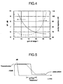
- a two stage EDFA included an input insertion loss of 2.2 dB, and was pumped at 980 nm using a pump feed-forward design.
- the dashed line shows the pump power required to achieve a 70% inversion level in the EDFA with approximately 29 dB of gain provided by the EDF.
- the solid line shows the noise figure of the device under the same conditions.
- Figure 4 clearly demonstrates the trade off between noise figure and pump utilization efficiency as the insertion loss location partitions the gain between the two stages of EDF.
- the figure points out that there is a limited range of locations in the gain path for the insertion loss where its impact on both noise figure performance and output power performance will be acceptable, and which will allow a desired or target noise figure performance and output power performance to be realized from the device.
- Example 1 illustrates an exemplary embodiment of the invention relating to suppression of crosstalk induced MPI.
Landscapes
- Physics & Mathematics (AREA)
- Electromagnetism (AREA)
- Engineering & Computer Science (AREA)
- Computer Networks & Wireless Communication (AREA)
- Signal Processing (AREA)
- Lasers (AREA)
- Optical Communication System (AREA)
Description
- This invention relates to multi-wavelength optical signal amplification devices and optical telecommunications systems utilizing such devices, and in particular to a dual amplification path (multichannel) optical amplifier having selectively located spectral filtering for suppressing crosstalk induced multipath interference (MPI), return loss (RL), and self oscillation, and which also provides for a desired level of noise figure performance and output power performance (i.e., pump utilization efficiency) notwithstanding increased filter insertion loss.
- The term "crosstalk" as used hereinafter will refer to an amplifier gain and reflection dependent phenomenon that is the genesis of multipath interference (MPI), return loss (RL), and self-oscillation, each of which are detrimental to good performance of a fiber optical communications system including an optical amplifier. The source of crosstalk induced MPI is illustrated in Figure 1, which very generically shows a bi-directional optical amplifier including a west-to-east optical signal transmission/amplification path 1-2-3 (where 1 and 3 are a west and east reflection, respectively, and 2 is a gain from west-to-east) for wavelengths Δλ1, for example, and an east-to-west optical signal transmission/amplification path 3-4-1 (where 4 is a gain from east-to-west) for wavelengths Δλ2. A Δλ1 MPI loop is represented by nodes 1-2-3-4-1 (i.e., Δλ1 input-G1-RE-G2-RW). Interference between originally transmitted Δλ1 signals and Δλ1 signals traversing the MPI loop gives rise to MPI. Likewise, node path 3-4-1-2-3 represents a Δλ2 MPI loop.
- Return loss (RL) refers to Δλ1 signals traversing nodal path 2-3-4 (i.e., G1-RE-G2), and/or Δλ2 signals traversing path 4-1-2, and represents the effective return reflectivity of the amplifier as seen by the communication system.
- Self oscillation in the amplifier (laser oscillation) will occur when a loop or cavity is set up in which the gain exceeds the losses. Therefore, e.g., if G1 + RW + G2 + RE > 0, then lasing will likely occur.
- Although the following specification will describe the invention in terms of a bi-directional (two counter-directional amplification paths) optical amplifier, the invention equally applies to a multichannel, unidirectional (two co-directional amplification paths) optical amplifier.
- A bi-directional optical signal amplifying device may typically provide a signal amplification path in substantially one direction (e.g., east to west) for one or more in-band communication channels within a particular frequency band (e.g., the "red" band or hereinafter, Δλ1), and a second signal amplifying path in a counter propagating direction (i.e., west to east) for one or more in-band communication channels in a different frequency band (e.g., "blue" band or hereinafter, Δλ2). Optical amplifiers used in optical communication transmission systems typically incorporate an optical isolator in the amplification path for filtering unwanted reflections or to suppress the build up of spontaneous emission, the effects of which impair amplifier and system performance. Although it is well known that most "all optical" amplifiers, such as erbium doped fiber amplifiers (EDFA's) and semiconductor amplifiers, for example, will amplify an input signal regardless of the direction that the signal enters the device, the use of an isolator in the amplification path essentially restricts such a device to substantially uni-directional operation. Optical amplifiers that are functionally bi-directional, on the other hand, and particularly those that include a substantially uni-directional amplification path for each counter propagating signal band, respectively, require means for primary signal routing through the respective counter directional amplification paths. The means for routing the primary counter propagating signals may include, for example, optical circulators or wavelength selective directional filters at each input/output port of the bi-directional amplifier. Optical circulators are not preferred primary signal routing components for use at the input/output of a bi-directional optical amplifier because they are not wavelength selective devices and they are expensive. Currently available wavelength selective directional filters, particularly single stage components, lack the capability to provide the desired degree of spectral band discrimination within a desired narrow spectral range. For instance, in an EDFA, the gain spectrum window is on the order of 30 nm (1530 - 1560 nm). As shown in Figure 1, a typical interference filter can provide approximately 10 dB spectral band discrimination through attenuation from reflection. This occurs, however, over a finite spectral range accompanied by a spectral "dead zone" of about 3 - 10 nm adjacent the signal band, instead of ideally as a step function, as shown in Figure 5. The dead zone thus reduces the communication signal channel availability in an already limited spectral window. Moreover, the 10 dB attenuation typically is not sufficient to eliminate MPI, RL and self oscillation effects due to, for example, reflected and double reflected Δλ2 light (from connectors or Rayleigh scattering) propagating in and being amplified by the primary amplification path for Δλ1 light, and vice-versa. More specifically, we have found that the most critical need for wavelength selective isolation in a bi-directional optical amplifying device is to suppress crosstalk induced MPI, RL, and self oscillation. Even with the use of isolators in the uni-directional amplification paths, MPI, for example, can occur due to light (e.g., in-band Δλ1) that propagates through the amplifier, gets reflected by some mechanism in an optical path of the system, and counter propagates through the amplifier along the primary amplification path for Δλ2 light (i.e., as out-of-band Δλ1, by going through the 10 dB wavelength selective routing filter via the nominally suppressed path for Δλ1), hitting another system reflection on the other side of the amplifier, and finally propagating again in the original intended direction of Δλ1 (as in-band Δλ1), to be reamplified. One proposed solution to this problem is to increase the spectral isolation at the amplifier input/output routing locations to the primary, substantially unidirectional amplification paths for the respective in-band signals by, for example, using multi-stage filters at the input/output ports of the amplifier. This, however, also introduces increased insertion loss into the device which is not preferable as it is well known to those skilled in the art that increasing the insertion loss at the input end of an optical amplifier results in an overall increase in noise figure (due to signal spontaneous beat noise) of the device, while increasing the insertion loss at the output end of the amplifier results in decreased output power for a given pump power.
- The inventors have therefore recognized a need for providing means for efficiently routing the respective communication signal bands into and out of the amplifier and, moreover, for suppressing unwanted (out-of-band) wavelength propagation through the amplifier that, if unsuppressed, results in crosstalk induced MPI, RL, and self oscillation, while not adversely impacting the noise figure and output power performance of the amplifier due to the increased insertion loss resulting from the spectral filtering.
- Cheng et al, in "622 Mb/S, 144 km Transmission Using a Bidirectional Fiber Amplifier Repeater", IEEE Photonics Technology Letters, (5), March 1993, pages 356-358, describe a repeater. Forward and back amplification paths each have a band pass filter inserted before an erbium doped fiber amplifier.
Barnard et al, in "Bidirectional Fiber Amplifiers", IEEE Photonics Technology Letters, August 1992, page 911 to 913, describe a bi-directional fiber amplifier. Optical band-pass filters are provided after erbium doped fiber amplifiers on forward and reverse amplification paths. - Additional features and advantages of the invention will be set forth in the description which follows, and in part will be apparent from the description, or may be learned by practice of the invention.
- According to a first aspect of the invention, there is provided an optical signal amplification device as described in appended
claim 1. - According to a second aspect of the invention, there is provided a method of improving the performance of a fiber optical telecommunication transmission system as described in appended claim 11.
- To achieve these and other advantages and in accordance with the purpose of the invention, as embodied and broadly described, an embodiment of the invention describes an optical signal amplification device having a substantially uni-directional first primary amplification path for amplifying an in-band wavelength band, Δλ1, and a second substantially unidirectional primary amplification path for amplifying a different in-band wavelength band, Δλ2, wherein at least one of the first and second amplification paths includes a wavelength selective insertion loss for substantially blocking the propagation of out-of-band signals in the amplification path, further wherein the location of the wavelength selective insertion loss in the amplification path is selected to provide either a target noise figure performance or output power performance from the device.
- In an aspect of this embodiment, the wavelength selective insertion loss is a dielectric optical interference filter. In alternative aspects of this embodiment, the wavelength selective insertion loss may be obtained from, for example, a fiber distributed Bragg reflector, a long period grating coupler filter, and a wavelength dependent fiber coupler device such as a twisted evanescent or multiclad type WDM device.
- In an aspect of the embodiment, the amplification path includes a rare earth doped optical fiber waveguide, such as an erbium doped fiber (EDF), for example. The invention, however, is not limited to fiber gain media, but may include a planar gain medium; and said gain media may include any of a variety of host glass compositions including silica, ZBLA(X), and oxyhalide (e.g., oxyfluoride) or glass-ceramic compositions having appropriate lasing dopants incorporated therein.
- In another embodiment, the invention describes a bi-directional optical signal amplification device that includes an input/output port for an optical signal band Δλ1 and for an optical signal band Δλ2, respectively, and another input/output port for an optical signal band Δλ2 and for an optical signal band Δλ1, respectively; a substantially unidirectional first primary amplification path for in-band Δλ1 including a waveguiding gain medium and a first wavelength selective insertion loss located along said gain medium for substantially blocking propagation of out-of-band Δλ2 along said first amplification path while substantially allowing propagation of in-band Δλ1 along said amplification path; a substantially unidirectional second primary amplification path for in-band Δλ2 including a waveguiding gain medium and a wavelength selective insertion loss located along said gain medium for substantially blocking the propagation of out-of-band Δλ1 along said second amplifying path while substantially allowing the propagation of in-band Δλ2 along said amplification path; first communication signals routing means coupled to the Δλ1- input/Δλ2 -output port and further coupled to said first amplification path for substantially directing said Δλ1 communication signals input to said port to said first amplification path; and second communication signals routing means coupled to said Δλ2 -input/Δλ1- output port and further coupled to said second amplification path for substantially directing said Δλ2 communication signals input to said port to said second amplification path. In an aspect of this embodiment, both the directional routing means and the wavelength selective insertion loss components can include, for example, a fiber distributed Bragg reflector, a long period grating coupler filter, and a wavelength dependent fiber coupler device such as a twisted evanescent or multiclad type WDM device.
- In another embodiment the invention describes an optical signal transmission system including a transmitter and a receiver and an optical amplifier having at least a first and a second substantially uni-directional primary amplification path for different inband wavelength bands, Δλ1 and Δλ2, respectively, wherein each said amplification path includes a waveguiding gain medium and a wavelength selective insertion loss located along said respective gain media for substantially preventing the propagation of an out-of-band optical communications signal along said respective amplification path, further wherein said wavelength selective insertion losses are located in their respective amplification paths to provide either a target noise figure performance or output power performance from the device.
- Another embodiment of the invention describes a method for suppressing crosstalk induced MPI, RL, and self oscillation in an optical amplifying device while maintaining a desired or target level of noise figure performance and output power performance of the device, including the steps of routing a communication signal substantially including an in-band wavelength band Δλ1 to a first substantially uni-directional gain path; providing a wavelength selective insertion loss in said gain path for substantially blocking the propagation of an out-of-band communication signals substantially including a wavelength band Δλ2 while substantially allowing the propagation of in-band Δλ1; routing a communication signal substantially including the in-band wavelength band Δλ2 to a second substantially uni-directional gain path; and providing a wavelength selective insertion loss in said second gain path for substantially blocking the propagation of out-of-band Δλ1 while substantially allowing the propagation of Δλ2, wherein said insertion losses are located in said respective gain paths to provide a pre-insertion loss gain and a post-insertion loss gain that provide either a desired or target noise figure performance and output power performance from the device.
- It is to be understood that both the foregoing general description and the following detailed description are exemplary and are intended to provide further explanation of the invention as claimed.
- The accompanying drawings are included to provide a further understanding of the invention and are incorporated in and constitute a part of this specification, illustrate embodiments of the invention and together with the description serve to explain the principles of the invention.
- Accordingly, the invention is directed to an apparatus and a method providing such features.
-
- Figure 1 is a schematic representation of a generic bi-directional optical signal amplification device having counter-directional amplification paths for respective in-band communication signal wavelength bands Δλ1 and Δλ2;
- Figure 2 is a more detailed view of one of the amplification paths of the device of Figure 1;
- Figures 3A and 3B are respective counter-directional, uni-directional amplifying paths of a bi-directional signal amplification device according to an embodiment of the invention, including a wavelength selective insertion loss located along the amplification path;
- Figure 4 is a graphical representation of the pump power (required to maintain a given output power) and noise figure (opposing y-axes) as a function of gain partitioning due to insertion loss location (x-axis) in an amplification path of an exemplary optical signal amplification device according to an embodiment of the invention;
- Figure 5 shows ideal (solid line) and practical (dashed line) transmission/attenuation curves for a conventional directional routing filter as a function of wavelength.
- Reference will now be made in detail to the present preferred embodiments of the invention, examples of which are illustrated in the accompanying drawings. Figure 1 shows a form of a generic bi-directional optical
signal amplification device 10 for guiding and amplifying optical signals in a first in-band wavelength band Δλ1, in a west to east direction and for simultaneously propagating and amplifying optical signals in a second in-band wavelength band Δλ2, in an east to west direction. Thedevice 10 comprises a first substantially unidirectionalprimary amplification path 21 for in-band wavelength band Δλ1, and a counter-directional, substantially unidirectional secondprimary amplification path 23 for in-band wavelength bandΔλ2, for amplifying and propagating respective optical signal wavelength bands Δλ1 and Δλ2, simultaneously, in opposite directions as shown. Amplifyingpaths primary amplification path signal gain medium fiber 31 and apumping source 37 coupled thereto by a fiberoptic coupler 35 or equivalent device known to those skilled in the art for coupling pump power into an active fiber. Anoptical isolator 39 is optionally located along theactive fiber waveguide 31 to block backward traveling light from entering the active fiber; i.e., to render the amplification path substantially unidirectional. The invention, however, is not limited to gain media comprising erbium doped fibers, but may alternatively comprise other rare earth doped fiber waveguides, planar amplifying waveguides that are well known in the art, or other fiber or planar waveguide compositions including oxyhalide (e.g., oxyfluoride) glass ceramics, ZBLA(X), and others known in the art. - Referring again to Figure 1, optical communications signals substantially comprising in-band Δλ1 approach the
device 10 from the west along transmission fiber 11W where they are input to the device via firstsignal routing filter 13.Filter 13 is designed to efficiently route a maximum amount of in-band Δλ1 input from the west toamplification path 21 and to allow a maximum amount of in-band Δλ2 input from the east alongpath 23 to get to transmission fiber 11W. Likewise, optical communications signals substantially comprising in-band Δλ2 approach thedevice 10 from the east along transmission fiber 11E where they are input to the device via secondsignal routing filter 15.Filter 15 is designed to efficiently route a maximum amount of in-band Δλ2 from transmission fiber 11E topath 23 and a maximum amount of in-band Δλ1 coming fromamplification path 21 to get to transmission fiber 11E. - Due to conventional filter technology limitations, filters 13, 15 will at best have a signal routing efficiency of about 90%; i.e., if
filter 13 is designed to direct a maximum amount of in-band Δλ1 signals topath 21 for propagation and amplification, it will be realized thatfilter 13 imparts about 10 dB insertion loss to the incoming signals, therefore about 10% of the input light is not directionally routed as intended but instead is transmitted topath 23 where it will typically be extinguished by an isolator (not shown). The in-band Δλ1 light that is directed by routingfilter 13 topath 21, and ultimately to east transmission fiber 11E viarouting filter 15, will inevitably be reflected, in part, back to routingfilter 15 due to system reflections including, but not limited to, splice misalignment, connectors and Rayleigh scattering. Although in a preferred embodiment of the invention filters 13, 15 are wavelength selective, a small portion of the reflected Δλ1 light along fiber 11E will be passed byfilter 15 to amplifying path 23 (as out-of-band Δλ1 light for this amplification path), whereupon it will be amplified bygain unit 19 and directed viafilter 13 in the west direction along transmission fiber 11W. This small amount of out-of-band Δλ1 light is not blocked byfilter 15 because of the non-ideal discrimination capability of the filter, a consequence of the small but finite (typically 10%) transmittance of the filter (for predominately reflected light). Additionally, due to the same filter limitations, light in the spectral dead band adjacent or in between, but not within, bands Δλ1 and Δλ2, can be routed along either amplification path, making the amplifier susceptible to self oscillation, for example, whereby any aggregate path gain exceeds the aggregate path loss resulting in the potential occurrence of laser action. A portion of the amplified out-of-band Δλ1 light frompath 23 traveling along fiber 11W will again inevitably be reflected by one or more reflection points along transmission fiber 11W whereupon a maximum amount of this reflected light will be reintroduced into primary amplifying path 21 (as in-band Δλ1 light) viarouting filter 13. This light will be amplified by amplifyingunit 17 and input into transmission fiber 11E in the east direction viafilter 15 as described above. This double reflected Δλ1 light will give rise to MPI with the originally transmitted Δλ1 light, likely to cause a degradation in system performance. It will be appreciated that the exact same phenomenon will occur with respect to Δλ2 light originally input to the device from the east. While it is appreciated that multiple, additional stages of insertion loss could be provided at the device input/output locations respective amplifying paths path 21 and out-of-band Δλ1 light from propagating alongpath 2 3, as shown in Figures 3a and 3b. In a preferred embodiment of the invention, wavelength selective filter means 41, 43 are dielectric interference filters similar tofilters - In addition to the spectral filtering characteristics of
filters filters 41, 42; i.e., how to partition the pre-insertion loss gain and the post-insertion loss gain. - Example 1, below, illustrates an exemplary embodiment of the invention relating to suppression of crosstalk induced MPI.
- Given the following parameter values:
- P (critical crosstalk gain limit; i.e., magnitude of the secondary pulse with respect to the primary pulse) = (-) 43 dB;
- GΔλ1 (i.e., gain for in-band Δλ1 signals along primary amplification path) = 27 dB;
- GΔλ2 (i.e., gain for in-band Δλ2 signals along primary amplification path) = 27 dB;
- Rworst case (i.e., worst case reflection requirement in a given direction) = (-)24 dB; and
- Gout-of-band Δλ1 (i.e., gain for out-of-band signals along an amplification path ) = 27 dB,
- It will be apparent to those skilled in the art that various modifications and variations can be made in the apparatus and method of the present invention without departing from scope of the invention. Thus, it is intended that the present invention cover the modifications and variations of this invention provided they come within the scope of the appended claims and their equivalents.

Claims (13)
- An optical signal amplification device, comprising:a substantially unidirectional first amplification path (21) for amplifying a first in-band communications signals wavelength band, Δλ1; anda substantially unidirectional second amplification path (23) for amplifying a second in-band communications signals wavelength band, Δλ2, different from Δλ1, and first communication signals routing means (13) for substantially directing input said in-band Δλ1 communication signals from a first transmission waveguide (11W) to said first amplification path (21) and amplified output said in-band Δλ2 communication signals to said transmission waveguide (11w); andsecond communication signals routing means (15) for substantially directing input said in-band Δλ2 communication signals from a second transmission waveguide (11E) to said second amplification path (23) and amplified output said in-band Δλ1 communication signals from said first amplification path to said second transmission waveguide (11E),wherein at least one of the first and second amplification paths (21, 23) includes a wavelength selective filtering means (41, 43) for substantially blocking an out-of-band optical communication signal,
characterised in that said wavelength selective filtering means (41, 43) is located along said at least one of the first and second amplification paths (21, 23) at a location that partitions the gain in said at least one of the first and second amplification paths (21, 23) such that gain is provided both before and after said wavelength selective filtering means (41, 43) for an in-band optical communication signal, for obtaining at least one of a target noise figure performance and a target output power performance from the optical signal amplification device;
wherein the insertion loss of said wavelength selective filtering means (41, 43) is selected to satisfy Ginband+Reast +Rwest+Gout of band <P where
Ginband is the gain for in-band signals in the in-band communications signals wavelength band along said at least one first and second amplification paths (21, 23),
Gout of band is the gain for the out-of-band signals along said at least one of the first and second amplification paths (21, 23) which include said wavelength filtering means (41, 43);
Reast and Rwest are the reflection losses occurring respectively at said first and second routing means (13, 15); and
P is a predetermined critical crosstalk gain limit. - The device of claim 1 wherein the wavelength selective filtering means (41, 43) is a dielectric optical interference filter, comprises a fiber distributed Bragg reflector, or is a long period grating coupler filter.
- The device of claim 1 wherein the wavelength selective filtering means (41, 43) is a wavelength dependent fiber coupler device including at least one of a twisted evanescent WDM device and a multiclad type WDM device.
- The device of claim 1 wherein at least one of the first and second amplification paths (21, 23) comprises a rare earth doped optical fiber waveguide (31).
- The device of claim 4 wherein the rare earth doped optical fiber waveguide (31) is doped with erbium.
- The device of claim 1 wherein at least one of the first and second amplification paths (21, 23) comprises a planar amplifying waveguide, or at least one of the first and second amplification paths (21, 23) comprises a glass ceramic composition, or an oxyhalide glass composition.
- The device of claim 1 wherein the first and second amplification paths (21, 23) are co-directional, or counter-directional.
- The device of claim 1 wherein the first communication signals in-band wavelength band, Δλ1, is from about 1520 - 1540 nm, and the second in-band communication signals wavelength band, Δλ2, is from about 1540 - 1570 nm, or wherein the first in-band communication signals wavelength band, Δλ1, is from about 1540 - 1570 nm, and the second in-band communication signals wavelength band, Δλ2, is from about 1520 - 1540 nm.
- The optical signal amplification device according to claim 1, further comprising:an input/output port for an optical communications signal band Δλ1 and for an optical communications signal band Δλ2, respectively; andan input/output port for an optical communications signal band Δλ2 and for an optical communications signal band Δλ1, respectively,wherein the substantially unidirectional first amplification path (21) includes a waveguiding gain medium (31) and the first wavelength selective filtering means (41) is located along said gain medium (31) for substantially blocking propagation of an out-of-band communications signal Δλ2 along said first amplification path while substantially allowing propagation of in-band Δλ1 along said first amplification path (21) and
the substantially unidirectional second amplification path (23) includes a waveguiding gain medium (31) and the second wavelength selective filtering means (43) is located along said gain medium (31) for substantially blocking propagation of an out-of-band communications signal Δλ1 along said second amplifying path while substantially allowing the propagation of in-band Δλ2 along said second amplification path (23). - An optical signal amplification device, according to claim 1, wherein the
first amplification path (21) has an input and an output end and includes a length of active fiber waveguide (31) substantially for propagating and amplifying an in-band communications signals wavelength band, Δλ1, and the first wavelength selective filter (41) located along the length of said active fiber (31) for substantially blocking the propagation and amplification of an out-of-band communications signals wavelength band, Δλ2 along the first amplifying path (21); and
the second amplification path (23) has an input and an output end and includes a length of active fiber waveguide (31) substantially for propagating and amplifying an in-band communications signals wavelength band, Δλ2, and the second wavelength selective filter (41) located along the length of said active fiber for substantially blocking the propagation and amplification of an out-of-band communications signals wavelength band, Δλ1 along the second amplifying path (23). - A method of improving the performance of a fiber optical telecommunication transmission system including an optical signal amplifying device having a substantially unidirectional first gain path (21) for amplifying a first in-band communications signal wavelength band Δλ1 and a substantially unidirectional second gain path (23) for amplifying a second in-band communications signal wavelength band Δλ2, different than Δλ1, comprising the steps of:routing a band of input Δλ1 communication signals from a first transmission waveguide (11w) to said first gain path (21) for amplification and propagation as in-band Δλ1 signals and amplified output in-band Δλ2 communication signals to said transmission waveguide;routing a band of input Δλ2 communication signals from a second transmission waveguide (11E) to said second gain path (23) for amplification and propagation as in-band Δλ2 signals and amplified output in-band Δλ, communications signals to said second transmission waveguide; andlocating a wavelength selective filtering means (41, 43) in at least one of the first gain path (21) and the second gain path (23) for blocking an out-of-band signal and being amplified thereby,characterised in that said wavelength selective filtering means (41, 43) is located along said at least one of the first and second gain paths (21, 23) at a location that partitions the gain in the first and second gain paths (21, 23) such that gain is provided both before and after said wavelength selective filtering means (41, 43) for an in-band optical communication signal, for obtaining at least one of the target noise figure performance and a target output power performance from the optical amplification device; and
wherein the insertion loss of said wavelength selective filtering means (41, 43) is selected to satisfy Ginband+ Reast+Rwest+Gout of band <P where Ginband is the gain for in-band signals in the in-band communications signals wavelength band along said at least one first and second gain paths (21, 23),
Gout of band is the gain for the out-of-band signals along said at least one of the first and second gain paths (21, 23) which include said wavelength filtering means (41, 43);
Reast and Rwest are the reflection losses occurring respectively at first and second routing means (13, 15); and
P is a predetermined critical crosstalk gain limit. - The method of claim 11 wherein routing the input in-band Δλ1 and the input in-band Δλ2 signals comprises directing a maximum amount of said signals to their respective gain paths (21, 23).
- The method of claim 11 wherein said wavelength selective filtering means (41, 43) block a maximum amount of out-of-band signals in each respective in-band gain path (21, 23).
Applications Claiming Priority (2)
| Application Number | Priority Date | Filing Date | Title |
|---|---|---|---|
| US3037896P | 1996-11-06 | 1996-11-06 | |
| US30378P | 1996-11-06 |
Publications (3)
| Publication Number | Publication Date |
|---|---|
| EP0841764A2 EP0841764A2 (en) | 1998-05-13 |
| EP0841764A3 EP0841764A3 (en) | 2000-01-26 |
| EP0841764B1 true EP0841764B1 (en) | 2006-12-20 |
Family
ID=21853937
Family Applications (1)
| Application Number | Title | Priority Date | Filing Date |
|---|---|---|---|
| EP97118514A Expired - Lifetime EP0841764B1 (en) | 1996-11-06 | 1997-10-24 | Crosstalk suppression in a multipath optical amplifier |
Country Status (11)
| Country | Link |
|---|---|
| US (2) | US6084704A (en) |
| EP (1) | EP0841764B1 (en) |
| JP (1) | JPH10190114A (en) |
| KR (1) | KR19980042118A (en) |
| CN (1) | CN1185067A (en) |
| AU (1) | AU720392B2 (en) |
| BR (1) | BR9705430A (en) |
| CA (1) | CA2217077A1 (en) |
| DE (1) | DE69737117T2 (en) |
| RU (1) | RU2185708C2 (en) |
| TW (1) | TW380209B (en) |
Families Citing this family (33)
| Publication number | Priority date | Publication date | Assignee | Title |
|---|---|---|---|---|
| US6084704A (en) * | 1996-11-06 | 2000-07-04 | Corning Incorporated | Crosstalk suppression in a multipath optical amplifier |
| US6052393A (en) | 1996-12-23 | 2000-04-18 | The Regents Of The University Of Michigan | Broadband Sagnac Raman amplifiers and cascade lasers |
| US6101024A (en) | 1998-03-24 | 2000-08-08 | Xtera Communications, Inc. | Nonlinear fiber amplifiers used for a 1430-1530nm low-loss window in optical fibers |
| US6356384B1 (en) | 1998-03-24 | 2002-03-12 | Xtera Communications Inc. | Broadband amplifier and communication system |
| US6631028B1 (en) * | 1998-03-24 | 2003-10-07 | Xtera Communications, Inc. | Broadband amplifier and communication system |
| US6600592B2 (en) | 1998-03-24 | 2003-07-29 | Xtera Communications, Inc. | S+ band nonlinear polarization amplifiers |
| US6597493B2 (en) | 2000-05-05 | 2003-07-22 | The Regents Of The University Of Michigan | Nonlinear fiber amplifiers used for a 1430-1530nm low-loss window in optical fibers |
| US6574037B2 (en) | 1998-06-16 | 2003-06-03 | Xtera Communications, Inc. | All band amplifier |
| US6885498B2 (en) | 1998-06-16 | 2005-04-26 | Xtera Communications, Inc. | Multi-stage optical amplifier and broadband communication system |
| US6618192B2 (en) | 1998-06-16 | 2003-09-09 | Xtera Communications, Inc. | High efficiency raman amplifier |
| US6469826B1 (en) | 1999-07-12 | 2002-10-22 | Nippon Telegraph And Telephone Corporation | Optical amplifier |
| US6826330B1 (en) * | 1999-08-11 | 2004-11-30 | Lightconnect, Inc. | Dynamic spectral shaping for fiber-optic application |
| US6587241B1 (en) * | 1999-08-20 | 2003-07-01 | Corvis Corporation | Optical protection methods, systems, and apparatuses |
| US6493133B1 (en) | 2000-06-30 | 2002-12-10 | Tyco Telecommunications (Us) Inc. | System and method for increasing capacity of undersea cables |
| US6417958B1 (en) * | 2001-01-24 | 2002-07-09 | Lucent Technologies Inc. | WDM optical communication system using co-propagating Raman amplification |
| JP4388705B2 (en) * | 2001-01-31 | 2009-12-24 | 富士通株式会社 | Optical amplifier |
| US6532101B2 (en) | 2001-03-16 | 2003-03-11 | Xtera Communications, Inc. | System and method for wide band Raman amplification |
| US6618193B1 (en) | 2001-03-26 | 2003-09-09 | Nortel Networks Limited | Optical amplification systems and methods |
| US6574406B2 (en) | 2001-09-11 | 2003-06-03 | Corning Incorporated | Selectively absorbing optical fibers for optical amplifiers |
| US6690508B2 (en) | 2002-03-26 | 2004-02-10 | Fujitsu Network Communications, Inc. | Control system and method for an optical amplifier |
| US8750702B1 (en) * | 2002-06-21 | 2014-06-10 | Rockstar Consortium Us Lp | Passive optical loopback |
| US7415206B1 (en) * | 2005-03-04 | 2008-08-19 | At&T Corp. | Arrangement for characterizing and reducing multi-path interference (MPI) and/or optical return loss (ORL) in optical transmission links having multiple discrete reflection sources |
| US8312033B1 (en) | 2008-06-26 | 2012-11-13 | Experian Marketing Solutions, Inc. | Systems and methods for providing an integrated identifier |
| JP5664295B2 (en) * | 2011-02-03 | 2015-02-04 | 富士通株式会社 | Communication device and communication device setting method |
| US9607336B1 (en) * | 2011-06-16 | 2017-03-28 | Consumerinfo.Com, Inc. | Providing credit inquiry alerts |
| WO2014090278A1 (en) * | 2012-12-10 | 2014-06-19 | Telefonaktiebolaget L M Ericsson (Publ) | Power control in bidirectional wdm optical link |
| US10664936B2 (en) | 2013-03-15 | 2020-05-26 | Csidentity Corporation | Authentication systems and methods for on-demand products |
| US9633322B1 (en) | 2013-03-15 | 2017-04-25 | Consumerinfo.Com, Inc. | Adjustment of knowledge-based authentication |
| US9721147B1 (en) | 2013-05-23 | 2017-08-01 | Consumerinfo.Com, Inc. | Digital identity |
| RU2623695C1 (en) * | 2015-12-24 | 2017-06-28 | Федеральное государственное бюджетное образовательное учреждение высшего образования "Владимирский Государственный Университет имени Александра Григорьевича и Николая Григорьевича Столетовых" (ВлГУ) | Method of suppressing spontaneous emission of quantum radiators in medium with dissipation |
| FR3079987A1 (en) * | 2018-04-06 | 2019-10-11 | Orange | METHOD OF PROCESSING A TRANSACTION BETWEEN A SOURCE TERMINAL AND A DESTINATION TERMINAL, BANKING SERVICE SYSTEM, TERMINAL AND CORRESPONDING COMPUTER PROGRAM. |
| US10911234B2 (en) | 2018-06-22 | 2021-02-02 | Experian Information Solutions, Inc. | System and method for a token gateway environment |
| US11941065B1 (en) | 2019-09-13 | 2024-03-26 | Experian Information Solutions, Inc. | Single identifier platform for storing entity data |
Family Cites Families (12)
| Publication number | Priority date | Publication date | Assignee | Title |
|---|---|---|---|---|
| JPS61162014A (en) * | 1985-01-10 | 1986-07-22 | Ricoh Co Ltd | Light source device for parallel laser beam |
| EP0419710A1 (en) * | 1989-09-28 | 1991-04-03 | Siemens Aktiengesellschaft | Bidirectional fibre-optical telecommunication system for wavelength division multiplexing between a central telecommunication station and a number of remote telecommunication stations |
| JPH0423628A (en) * | 1990-05-18 | 1992-01-28 | Nec Corp | Optical repeater |
| DE69224340T2 (en) * | 1991-09-30 | 1998-06-04 | Nippon Electric Co | Two-way repeater with optical amplification |
| US5280549A (en) * | 1993-02-05 | 1994-01-18 | National Research Council Of Canada | Frequency dependent optical isolator |
| US5430572A (en) * | 1993-09-30 | 1995-07-04 | At&T Corp. | High power, high gain, low noise, two-stage optical amplifier |
| WO1995015625A1 (en) * | 1993-12-01 | 1995-06-08 | Williams Telecommunications Group, Inc. | Bidirectional optical amplifier |
| US5513029A (en) * | 1994-06-16 | 1996-04-30 | Northern Telecom Limited | Method and apparatus for monitoring performance of optical transmission systems |
| US5742416A (en) * | 1996-03-28 | 1998-04-21 | Ciena Corp. | Bidirectional WDM optical communication systems with bidirectional optical amplifiers |
| US5815308A (en) * | 1996-05-20 | 1998-09-29 | Northern Telecom Limited | Bidirectional optical amplifier |
| US5812306A (en) * | 1996-06-14 | 1998-09-22 | Ciena Corporation | Bidirectional WDM optical communication systems with bidirectional optical amplifiers |
| US6084704A (en) * | 1996-11-06 | 2000-07-04 | Corning Incorporated | Crosstalk suppression in a multipath optical amplifier |
-
1997
- 1997-09-09 US US08/925,918 patent/US6084704A/en not_active Expired - Lifetime
- 1997-09-26 CA CA002217077A patent/CA2217077A1/en not_active Abandoned
- 1997-10-24 EP EP97118514A patent/EP0841764B1/en not_active Expired - Lifetime
- 1997-10-24 DE DE69737117T patent/DE69737117T2/en not_active Expired - Fee Related
- 1997-11-05 AU AU44345/97A patent/AU720392B2/en not_active Ceased
- 1997-11-05 RU RU97118611/09A patent/RU2185708C2/en not_active IP Right Cessation
- 1997-11-05 KR KR1019970058245A patent/KR19980042118A/en not_active Ceased
- 1997-11-06 BR BR9705430A patent/BR9705430A/en not_active IP Right Cessation
- 1997-11-06 JP JP9304248A patent/JPH10190114A/en active Pending
- 1997-11-06 CN CN97122507A patent/CN1185067A/en active Pending
-
1998
- 1998-01-23 TW TW087101144A patent/TW380209B/en not_active IP Right Cessation
-
2000
- 2000-05-23 US US09/576,663 patent/US6342966B1/en not_active Expired - Lifetime
Non-Patent Citations (1)
| Title |
|---|
| SMART R G ET AL.: "TWO-STAGE ERBIUM-DOPED FIBRE AMPLIFIERS SUITABLE FOR USE IN LONG-HAUL SOLITON SYSTEMS", ELECTRONICS LETTERS, IEE STEVENAGE, GB, vol. 30, no. 1, 6 January 1994 (1994-01-06), pages 50 - 52, XP000424692, DOI: doi:10.1049/el:19940023 * |
Also Published As
| Publication number | Publication date |
|---|---|
| AU4434597A (en) | 1998-05-14 |
| EP0841764A2 (en) | 1998-05-13 |
| KR19980042118A (en) | 1998-08-17 |
| US6084704A (en) | 2000-07-04 |
| US6342966B1 (en) | 2002-01-29 |
| BR9705430A (en) | 1999-06-29 |
| CN1185067A (en) | 1998-06-17 |
| JPH10190114A (en) | 1998-07-21 |
| TW380209B (en) | 2000-01-21 |
| MX9708539A (en) | 1998-09-30 |
| EP0841764A3 (en) | 2000-01-26 |
| CA2217077A1 (en) | 1998-05-06 |
| AU720392B2 (en) | 2000-06-01 |
| RU2185708C2 (en) | 2002-07-20 |
| DE69737117T2 (en) | 2007-07-05 |
| DE69737117D1 (en) | 2007-02-01 |
Similar Documents
| Publication | Publication Date | Title |
|---|---|---|
| US6342966B1 (en) | Crosstalk suppression in a multipath optical amplifier | |
| KR100387072B1 (en) | Bidirectional Optical Amplifier | |
| US5790300A (en) | Multi-channel fiber amplification system and associated method | |
| RU97118611A (en) | CROSS DISTORTION SUPPRESSION IN A MULTI-CHANNEL OPTICAL AMPLIFIER | |
| JPH04318526A (en) | Optical fiber amplifier | |
| EP1068684A2 (en) | Optical fiber amplifier having a gain flattening filter | |
| US6031646A (en) | Optical fiber telecommunication system | |
| EP0881723B1 (en) | Hybrid fiber amplifier | |
| WO2003065625A2 (en) | Fiber ring amplifiers and lasers | |
| US5801879A (en) | Device and method to supress Q-switching in an optical amplifying device | |
| CA2492810C (en) | Multi-stage raman amplifier | |
| US6618193B1 (en) | Optical amplification systems and methods | |
| US6862132B1 (en) | Suppression of double rayleigh backscattering and pump reuse in a raman amplifier | |
| CA2353762C (en) | Optical transmission link incorporating highpass optical filtering | |
| JP2859386B2 (en) | Bidirectional optical fiber amplifier | |
| JP4661027B2 (en) | Noise light removal device | |
| JPH11122171A (en) | Wavelength dispersion compensation type optical amplifier and optical communication system using the same | |
| CN117080847A (en) | Optical amplifier, optical amplification method and optical fiber communication system | |
| RU2172562C2 (en) | Bi-directional optical amplifier and manner of bi-directional communication | |
| AU711376B2 (en) | Hybrid fiber amplifier | |
| MXPA97008539A (en) | Suppression of diaphony in an optical amplifier of vias multip | |
| JPH03192221A (en) | Optical active module | |
| JPH08162696A (en) | Optical amplifier |
Legal Events
| Date | Code | Title | Description |
|---|---|---|---|
| PUAI | Public reference made under article 153(3) epc to a published international application that has entered the european phase |
Free format text: ORIGINAL CODE: 0009012 |
|
| AK | Designated contracting states |
Kind code of ref document: A2 Designated state(s): BE CH DE DK ES FR GB IE IT LI SE |
|
| AX | Request for extension of the european patent |
Free format text: AL;LT;LV;RO;SI |
|
| PUAL | Search report despatched |
Free format text: ORIGINAL CODE: 0009013 |
|
| AK | Designated contracting states |
Kind code of ref document: A3 Designated state(s): AT BE CH DE DK ES FI FR GB GR IE IT LI LU MC NL PT SE |
|
| AX | Request for extension of the european patent |
Free format text: AL;LT;LV;RO;SI |
|
| 17P | Request for examination filed |
Effective date: 20000628 |
|
| AKX | Designation fees paid |
Free format text: BE CH DE DK ES FR GB IE IT LI SE |
|
| 17Q | First examination report despatched |
Effective date: 20011214 |
|
| RAP1 | Party data changed (applicant data changed or rights of an application transferred) |
Owner name: AVANEX CORPORATION |
|
| GRAP | Despatch of communication of intention to grant a patent |
Free format text: ORIGINAL CODE: EPIDOSNIGR1 |
|
| GRAS | Grant fee paid |
Free format text: ORIGINAL CODE: EPIDOSNIGR3 |
|
| GRAA | (expected) grant |
Free format text: ORIGINAL CODE: 0009210 |
|
| AK | Designated contracting states |
Kind code of ref document: B1 Designated state(s): BE CH DE DK ES FR GB IE IT LI SE |
|
| PG25 | Lapsed in a contracting state [announced via postgrant information from national office to epo] |
Ref country code: LI Free format text: LAPSE BECAUSE OF FAILURE TO SUBMIT A TRANSLATION OF THE DESCRIPTION OR TO PAY THE FEE WITHIN THE PRESCRIBED TIME-LIMIT Effective date: 20061220 Ref country code: DK Free format text: LAPSE BECAUSE OF FAILURE TO SUBMIT A TRANSLATION OF THE DESCRIPTION OR TO PAY THE FEE WITHIN THE PRESCRIBED TIME-LIMIT Effective date: 20061220 Ref country code: CH Free format text: LAPSE BECAUSE OF FAILURE TO SUBMIT A TRANSLATION OF THE DESCRIPTION OR TO PAY THE FEE WITHIN THE PRESCRIBED TIME-LIMIT Effective date: 20061220 Ref country code: BE Free format text: LAPSE BECAUSE OF FAILURE TO SUBMIT A TRANSLATION OF THE DESCRIPTION OR TO PAY THE FEE WITHIN THE PRESCRIBED TIME-LIMIT Effective date: 20061220 |
|
| REG | Reference to a national code |
Ref country code: GB Ref legal event code: FG4D |
|
| REG | Reference to a national code |
Ref country code: CH Ref legal event code: EP |
|
| REF | Corresponds to: |
Ref document number: 69737117 Country of ref document: DE Date of ref document: 20070201 Kind code of ref document: P |
|
| REG | Reference to a national code |
Ref country code: IE Ref legal event code: FG4D |
|
| PG25 | Lapsed in a contracting state [announced via postgrant information from national office to epo] |
Ref country code: SE Free format text: LAPSE BECAUSE OF FAILURE TO SUBMIT A TRANSLATION OF THE DESCRIPTION OR TO PAY THE FEE WITHIN THE PRESCRIBED TIME-LIMIT Effective date: 20070320 |
|
| PG25 | Lapsed in a contracting state [announced via postgrant information from national office to epo] |
Ref country code: ES Free format text: LAPSE BECAUSE OF FAILURE TO SUBMIT A TRANSLATION OF THE DESCRIPTION OR TO PAY THE FEE WITHIN THE PRESCRIBED TIME-LIMIT Effective date: 20070331 |
|
| REG | Reference to a national code |
Ref country code: CH Ref legal event code: PL |
|
| ET | Fr: translation filed | ||
| PLBE | No opposition filed within time limit |
Free format text: ORIGINAL CODE: 0009261 |
|
| STAA | Information on the status of an ep patent application or granted ep patent |
Free format text: STATUS: NO OPPOSITION FILED WITHIN TIME LIMIT |
|
| 26N | No opposition filed |
Effective date: 20070921 |
|
| PG25 | Lapsed in a contracting state [announced via postgrant information from national office to epo] |
Ref country code: IE Free format text: LAPSE BECAUSE OF NON-PAYMENT OF DUE FEES Effective date: 20071024 |
|
| PGFP | Annual fee paid to national office [announced via postgrant information from national office to epo] |
Ref country code: DE Payment date: 20081201 Year of fee payment: 12 |
|
| PGFP | Annual fee paid to national office [announced via postgrant information from national office to epo] |
Ref country code: IT Payment date: 20081025 Year of fee payment: 12 |
|
| PG25 | Lapsed in a contracting state [announced via postgrant information from national office to epo] |
Ref country code: DE Free format text: LAPSE BECAUSE OF NON-PAYMENT OF DUE FEES Effective date: 20100501 |
|
| PG25 | Lapsed in a contracting state [announced via postgrant information from national office to epo] |
Ref country code: IT Free format text: LAPSE BECAUSE OF NON-PAYMENT OF DUE FEES Effective date: 20091024 |
|
| PGFP | Annual fee paid to national office [announced via postgrant information from national office to epo] |
Ref country code: GB Payment date: 20131023 Year of fee payment: 17 |
|
| REG | Reference to a national code |
Ref country code: GB Ref legal event code: 732E Free format text: REGISTERED BETWEEN 20140116 AND 20140122 |
|
| PGFP | Annual fee paid to national office [announced via postgrant information from national office to epo] |
Ref country code: FR Payment date: 20141017 Year of fee payment: 18 |
|
| GBPC | Gb: european patent ceased through non-payment of renewal fee |
Effective date: 20141024 |
|
| PG25 | Lapsed in a contracting state [announced via postgrant information from national office to epo] |
Ref country code: GB Free format text: LAPSE BECAUSE OF NON-PAYMENT OF DUE FEES Effective date: 20141024 |
|
| REG | Reference to a national code |
Ref country code: FR Ref legal event code: TP Owner name: II-VI INCORPORATED, US Effective date: 20160316 Ref country code: FR Ref legal event code: CD Owner name: II-VI INCORPORATED, US Effective date: 20160316 Ref country code: FR Ref legal event code: CA Effective date: 20160316 |
|
| REG | Reference to a national code |
Ref country code: FR Ref legal event code: ST Effective date: 20160630 |
|
| PG25 | Lapsed in a contracting state [announced via postgrant information from national office to epo] |
Ref country code: FR Free format text: LAPSE BECAUSE OF NON-PAYMENT OF DUE FEES Effective date: 20151102 |