EP0838978B1 - Low-loss electrical interconnects - Google Patents
Low-loss electrical interconnects Download PDFInfo
- Publication number
- EP0838978B1 EP0838978B1 EP97122728A EP97122728A EP0838978B1 EP 0838978 B1 EP0838978 B1 EP 0838978B1 EP 97122728 A EP97122728 A EP 97122728A EP 97122728 A EP97122728 A EP 97122728A EP 0838978 B1 EP0838978 B1 EP 0838978B1
- Authority
- EP
- European Patent Office
- Prior art keywords
- conductive
- wad
- contact element
- contact
- members
- Prior art date
- Legal status (The legal status is an assumption and is not a legal conclusion. Google has not performed a legal analysis and makes no representation as to the accuracy of the status listed.)
- Expired - Lifetime
Links
Images



Classifications
-
- H—ELECTRICITY
- H01—ELECTRIC ELEMENTS
- H01R—ELECTRICALLY-CONDUCTIVE CONNECTIONS; STRUCTURAL ASSOCIATIONS OF A PLURALITY OF MUTUALLY-INSULATED ELECTRICAL CONNECTING ELEMENTS; COUPLING DEVICES; CURRENT COLLECTORS
- H01R13/00—Details of coupling devices of the kinds covered by groups H01R12/70 or H01R24/00 - H01R33/00
- H01R13/02—Contact members
- H01R13/22—Contacts for co-operating by abutting
- H01R13/24—Contacts for co-operating by abutting resilient; resiliently-mounted
- H01R13/2407—Contacts for co-operating by abutting resilient; resiliently-mounted characterized by the resilient means
-
- H—ELECTRICITY
- H01—ELECTRIC ELEMENTS
- H01R—ELECTRICALLY-CONDUCTIVE CONNECTIONS; STRUCTURAL ASSOCIATIONS OF A PLURALITY OF MUTUALLY-INSULATED ELECTRICAL CONNECTING ELEMENTS; COUPLING DEVICES; CURRENT COLLECTORS
- H01R12/00—Structural associations of a plurality of mutually-insulated electrical connecting elements, specially adapted for printed circuits, e.g. printed circuit boards [PCB], flat or ribbon cables, or like generally planar structures, e.g. terminal strips, terminal blocks; Coupling devices specially adapted for printed circuits, flat or ribbon cables, or like generally planar structures; Terminals specially adapted for contact with, or insertion into, printed circuits, flat or ribbon cables, or like generally planar structures
- H01R12/70—Coupling devices
- H01R12/71—Coupling devices for rigid printing circuits or like structures
- H01R12/712—Coupling devices for rigid printing circuits or like structures co-operating with the surface of the printed circuit or with a coupling device exclusively provided on the surface of the printed circuit
- H01R12/714—Coupling devices for rigid printing circuits or like structures co-operating with the surface of the printed circuit or with a coupling device exclusively provided on the surface of the printed circuit with contacts abutting directly the printed circuit; Button contacts therefore provided on the printed circuit
-
- H—ELECTRICITY
- H01—ELECTRIC ELEMENTS
- H01R—ELECTRICALLY-CONDUCTIVE CONNECTIONS; STRUCTURAL ASSOCIATIONS OF A PLURALITY OF MUTUALLY-INSULATED ELECTRICAL CONNECTING ELEMENTS; COUPLING DEVICES; CURRENT COLLECTORS
- H01R13/00—Details of coupling devices of the kinds covered by groups H01R12/70 or H01R24/00 - H01R33/00
- H01R13/02—Contact members
- H01R13/22—Contacts for co-operating by abutting
- H01R13/24—Contacts for co-operating by abutting resilient; resiliently-mounted
-
- H—ELECTRICITY
- H01—ELECTRIC ELEMENTS
- H01R—ELECTRICALLY-CONDUCTIVE CONNECTIONS; STRUCTURAL ASSOCIATIONS OF A PLURALITY OF MUTUALLY-INSULATED ELECTRICAL CONNECTING ELEMENTS; COUPLING DEVICES; CURRENT COLLECTORS
- H01R13/00—Details of coupling devices of the kinds covered by groups H01R12/70 or H01R24/00 - H01R33/00
- H01R13/02—Contact members
- H01R13/33—Contact members made of resilient wire
-
- H—ELECTRICITY
- H05—ELECTRIC TECHNIQUES NOT OTHERWISE PROVIDED FOR
- H05K—PRINTED CIRCUITS; CASINGS OR CONSTRUCTIONAL DETAILS OF ELECTRIC APPARATUS; MANUFACTURE OF ASSEMBLAGES OF ELECTRICAL COMPONENTS
- H05K3/00—Apparatus or processes for manufacturing printed circuits
- H05K3/30—Assembling printed circuits with electric components, e.g. with resistors
- H05K3/32—Assembling printed circuits with electric components, e.g. with resistors electrically connecting electric components or wires to printed circuits
- H05K3/325—Assembling printed circuits with electric components, e.g. with resistors electrically connecting electric components or wires to printed circuits by abutting or pinching; Mechanical auxiliary parts therefor
-
- H—ELECTRICITY
- H05—ELECTRIC TECHNIQUES NOT OTHERWISE PROVIDED FOR
- H05K—PRINTED CIRCUITS; CASINGS OR CONSTRUCTIONAL DETAILS OF ELECTRIC APPARATUS; MANUFACTURE OF ASSEMBLAGES OF ELECTRICAL COMPONENTS
- H05K3/00—Apparatus or processes for manufacturing printed circuits
- H05K3/36—Assembling printed circuits with other printed circuits
- H05K3/368—Assembling printed circuits with other printed circuits parallel to each other
Definitions
- the present invention relates to electronic circuit interconnection, and more particularly to an electrical connector having the features of the preamble portion of claim 1.
- wadded conductor contacts or “buttons” mounted in insulator substrates to form “button boards” is a known type of interface device for electronic circuit coupling. They typically provide both direct coupling and physical separation between electronic circuits, which are commonly formed on adjacent circuit boards. Most frequently, resilient bundles or “wads” of fine electric current conductors are retentively engaged in corresponding holes in or passing through the non-conductive substrate board. The ends of these wads or “buttons” are exposed and typically protrude at the respective surface of the insulative carrier board; see for example U.S. Patents No. 4,581,679 and 4,574,331. Such conductive wads have very low resistance to current when their exposed ends or “buttons” are compressively engaged with surface contact pad areas on the circuit boards.
- wadded conductor elements have relatively low capacitance and inductance, and so they provide relatively low impedance for dynamic electronic circuit configurations, such as are used for high speed data processing and other high bandwidth applications.
- buttons are technically superior to many other electronic circuit interconnection arrangements
- previously proposed designs have presented a number of practical problems in their fabrication and use.
- cylindrical button contacts of wadded fine conductor wires have been inserted axially into generally uniform cylindrical holes which were formed in the substrate such as by acid etching of ceramicized glass substrates or drilling a laminated or sheet plastic insulator sheet.
- the button wads fill the respective holes and are held in place in their corresponding holes by compressive radial frictional engagement with the side walls of each of the holes. Because of this relationship, insertion of the button wads into their respective holes has been a difficult process.
- the threshhold problem was in feeding or threading the leading end of each wad into the respective hole.
- the resulting frictional engagement of the wads with the holes impaired the spring movement of the contacts and hence reduced the effective desirable resiliency of the inserted wads. This was especially true when the holes were formed by etching or drilling, because any roughness or surface discontinuities on the hole walls increased the friction and/or catching of the fine conductors of the contact wads on the walls of the holes.
- the impairment of spring action movement of the contacts could adversely effect the positioning of the contact ends and cause variances in the compressive engagement of the multiple conductive strand elements making up the contact end surface with an opposed conductive contact surface, with attendant unpredictability of the electrical resistance through the resulting contact interface.
- any strand segment or segments of the contact which were misaligned with the respective hole either because of spreading or “mushrooming" of the protruding contact end or any pulling or other lateral detachment or displacement of a strand segment from the cylindrical contact body became "loose strands" which could be caught between the substrate and the adjacent mating components. This would preclude proper surface-to-surface seating of the component on the substrate and correspondingly limit the compressive force on the main body of the contact and also effect the resultant electrical resistance through the contacts.
- Such loose strands also can cause short circuits to adjacent conductors on the interconnect substrate or on the respective mating component, such as a circuit board.
- the lack of free movement of the contact ends can also cause the buttons to shift off center when compressed in use.
- buttons will not be as securely retained in the hole, and the buttons can be easily dislodged during handling and, in some instances, during use.
- a primary object of the present invention is to provide improved interconnects using wadded conductor contact elements and which overcome the aforenoted problems.
- More specific objects are to reduce insertion resistance for placement of conductor button wads into corresponding holes of an interconnect substrate and to provide consistent predictable spring action movement of the end portions of the wads.
- Another object of the invention is to retain each contact wad in its corresponding hole during assembly and shipment.
- Still other objects of the invention are to assure reception of all strands of the button wad end within the respective hole in the substrate, and to prevent short circuits between each button and other conductive elements of associated components.
- a further object of the invention is to improve the axial centering of the buttons during compression between associated contacts.
- a still further object of the invention is to increase the possible insertion length for the wads to allow thick button boards to be fabricated.
- the present invention includes a button board configuration with specially shaped holes through the board, which provides easier insertion of the wadded conductor contact elements.
- the lower resistance to wad insertion aids in fully seating the wads within their respective holes. It also avoids undue impairment of the resilient movement of the contact portions of the buttons, prevents adverse effects of "loose strands" and minimizes the likelihood of off-center shift. It also allows long contact wads to be fully inserted into holes in very thick button boards.
- the wad receiving holes are configured to have constriction/retention zones of minimum length and enlarged end portions which allow unrestricted movement of the contact end portions of each wad.
- the end portions of the holes are chamfer-tapered, or chamfer-tapered and countersunk, to facilitate wad insertion as well as lower insertion resistance. Because of the additional wad-to-hole wall clearance provided on each hole end, the button wads retain more effective resilience when compressed by associated surface contacts and their strands are able to expand laterally without overlapping the substrate around their respective holes, thereby preventing interference with abutment positioning of mating components and also prevent unintentional short circuits to adjacent conductive elements.
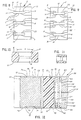
- Figure 1 is an enlarged perspective view of a button board.
- Figure 2 is a cross-sectional view of the button board along line 2-2 in Figure 1.
- Figures 3 is a corresponding view of the board substrate shown in Figure 2.
- Figure 4 is a cross-sectional view corresponding to Figure 2.
- Figures 5 is a corresponding view of the board substrate in Figure 4.
- Figure 6 is a sectional view of an interconnect assembly coupled to associated circuit boards.
- Figure 7 is a sectional view of an interconnect assembly incorporating an embodiment of the invention coupled to associated circuit boards with modified forms of contact interfaces.
- Figure 8 is a button board incorporating the invention with recessed buttons along one contact surface.
- Figure 9 is a button board incorporating the invention with recessed buttons along both contact surfaces.
- Figures 10 and 11 are further enlarged sectional views of board substrate section illustrating in greater detail examples of suitable cavity or hole configurations.
- FIGS 12, 13, 14 and 15 are sectional views of other contact interface assemblies employing teachings of this invention, the latter four illustrating the inclusion of movable plunger-type contact elements associated with the buttons.
- Figures 1 and 2 show a representational electrical circuit interface assembly in the form of a button board assembly 2.
- the assembly 2 includes an electrical insulator substrate board or carrier 4, which although shown as generally rectangular, may have any other desired shape, such as cylindrical or tubular. Also, the relative thickness of the carrier and length of the contact wads are exaggerated in these drawings.
- the carrier 4 is a thin flat rigid or semi-rigid planar sheet or board and the contact wads are correspondingly short, being of slightly greater relaxed length than the thickness dimension of the carrier 4.
- the carrier 4 has a thickness in the range of 0.0508 to 0.2794 cm (0.020 to 0.110 inch).
- the carrier 4 includes at least one hole 6 therethrough, but typically there are a plurality of holes 6 arranged about the board in an array, such as a grid pattern, chosen to correspond to the potential locations of circuit interconnection between associated electronic circuit interconnection contacts with which the assembly 2 is to be used.
- the holes 6 extend from a first surface 8 of the carrier 4 to a second surface 10 of the carrier 4, with the second surface 10 typically being opposite and parallel to the first surface 8.
- the hole 6 at each location where an interconnection is desired contains a resilient contact button "wad” 12.
- Each of the wads 12 comprises a resiliently wadded conductor, typically in the form of an elongated cylindrical contact element comprising a resiliently and randomly wadded single thin gauge electrically conductive wire.
- the wads 12 may be of the type commercially marketed by Tecknit of Cranford, New Jersey under the designation "Fuzz Button” and by AmCon of Hawthorne, California under the designation "Button Contact”.
- the wads 12 extend generally from at least the first surface 8 to the second surface 10, and protrude slightly beyond both the first surface 8 and the second surface 10.
- the ends of each of the wads 12 exposed at the first surface 8 and the second surface 10 comprise button contacts 14 of the button board assembly 2.
- FIG. 2 A cross-sectional view of the button board 2 in Figure 1 along line 2-2, is shown in Figure 2.
- Each of the holes 6 has a short central straight cylindrical section 16 intermediate the first surface 8 and the second surface 10.
- This section 16 is smaller in cross-sectional configuration and/or dimensions than the nominal relaxed cross-section of the wads 12 for compressive frictional engagement of the respective wad to retain the wad 12 in the carrier 4 during handling and, where necessary, during use.
- the end of the central straight section 16 closest to the first surface 8 joins a first chamfer-tapered section 18 which extends to the first surface 8 with a first included chamfer angle.
- the other end of the central straight section 16 closest to the second surface 10 joins a second chamfer-tapered section 20 which extends to the second surface 10 and has a second included chamfer angle.
- the cross sectional configuration and size of the tapered sections preferably are such that the wad 12 is free of engagement with those walls over a substantial portion of its axial length adjacent each end.
- the outer openings at the surfaces 8 and 10 are substantially larger than the cross-section of the wads 12.
- the respective lengths of the central straight section 16, the first tapered section 18 and the second tapered section 20 may be proportioned, as well as the angles of the first and second chamfer angles, depending upon the thickness of the carrier 4, the diameter of the wads 12, the necessary engagement forces for retaining the button wads in the carrier during handling and service, and the desired resiliency of the contacts, as explained in greater detail below.
- the carrier 4 preferably is molded or machined with the configuration for the holes 6 as shown in Figure 2.
- the carriers 4 may be formed by injection molding of suitable electrically insulating materials. Those materials should have good flow characteristics at molding temperatures to assure formation of the fine detail required for the small hole configurations, particularly when molding thin carriers 4.
- Core pins of complementary configuration define the holes of the selected configuration in the molds.
- suitable moldable materials include polyesters, such as the product sold by E.I. DuPont de Nemours & Co. under the tradename Rynite and liquid crystal polymers such as the product marketed by Hoechst Celanese Corporation under the tradename Vectra. Smooth inner wall surfaces of the holes are assured by a molding process, even when glass fiber fillers are included to enhance the stability of the final board product.
- the desired hole configuration is also easily secured with a carrier 4 which is suitably machined from a solid sheet or board.
- the hole 6 is bored completely through the carrier 4 so that it extends from the first surface 8 to the second surface 10 with a diameter corresponding to that desired for the central section 16.
- the first tapered section 18 is formed in the hole 6 by chamfering the hole 6 to the desired depth and first slope angle from the first surface 8.
- the second tapered section 20 is formed in the hole 6 by chamfering the hole 6 to the desired depth and second chamfer angle from the second surface 10 thereby completing this configuration for the hole 6 with the first tapered section 18, the second tapered section 20 and the central straight section 16 therebetween. Forming the holes by such machining usually is more economical for short production runs.
- the wad 12 for each of the holes 6 may be inserted through either the first tapered section 18 or the second tapered section 20 and pushed through the hole 6 until it seats as desired, as shown in Figure 2.
- the enlarged outer ends and respective tapers of the end sections facilitate the entry of each wad into the respective hole and prevent the individual conductors in the wad 12 from catching on the wall of the hole 6 as the wad 12 is inserted. They also reduce insertion resistance because the wad 12 is only compressively engaged in the hole 6 along the length of the central straight section 16, due to its relatively narrow diameter. Both the lengths and the chamfer angles of the first tapered section 18 and the second tapered section 20 determine the resiliency of their respective button contact end portion, as described in detail below.
- FIG 4 shows a cross-sectional view of the button board 2 corresponding to Figure 2 with this alternate configuration for the holes 6.
- Each of the holes 6 has the central straight section 16 intermediate the first surface 8 and the second surface 10.
- the end of the central straight section 16 closest to the first surface 8 joins with the first tapered section 18, as described above in connection with Figure 2.
- the other end of the central straight section 16 joins with a second straight section 22 which extends to the second surface 10 and has a uniform counterbore diameter greater than the diameter of the hole 6 represented by the diameter of the central section 16.
- the respective lengths of the first tapered section 18, the central straight section 16 and the second straight section 22 may be proportioned, as well as the first chamfer angle proportioned and counterbore diameter sized, depending upon the thickness of the carrier 4, the diameter of the wads 12 and the desired resiliency of the button contacts 14, as explained in further detail below.
- the carrier 4 may be molded with the configuration for the holes 6 as shown in Figure 4, or machined, as noted above.
- the wad 12 for each of the holes 6 preferably is inserted into the first tapered section 18 and pushed through the hole 6 until it seats as desired, as shown in Figure 6.
- the taper of the first section 18 facilitates entry of the wad 12 into the end opening of the hole and reduces the area in which the individual conductors in the wad 12 can catch on the wall of the hole 6 as the wad 12 is inserted.
- the first tapered section 18 and the second straight section 22 both reduce insertion resistance because the wad 12 is only compressively engaged in the hole 6 along the length of the central straight section 16, because of its relatively narrow diameter.
- the lengths of the first tapered section 18 and the second straight section 22 determine the resiliency of their respective button contact end portions, as do the clearance between the ends of the wad 12 with the respective walls of the first tapered section 18 and the second straight section 22, as explained in more detail below.
- the operation of the configuration of Figure 2 is shown in Figure 6.
- the button board 2 is sandwiched between a first circuit board 24 and a second circuit board 26.
- the first circuit board 24 has an electrically insulated first board barrier 28 carrying electrical circuitry elements with at least one first board surface contact 30, but typically a plurality of the first board surface contacts 30.
- Each one of the surface contacts 30 is located to coincidentally abut one corresponding button end 14 of a different one of the wads 12 in the button board 2.
- the surface contacts 30 are relatively broad thin flat conductive contact areas or "pads" on the respective exposed surface of the circuit board.
- the button contacts 14 in abutment contact with the surface contacts 30 are pressed inwardly relative to the surface of the carrier 4 whereby the button is resiliently compressed essentially to the point of co-planar relation with the respective surface 8 or 10 as shown in Figure 6.
- the surface contacts 30 have extremely thin contact surfaces, typically in the range of 0.00381 to 0.00762 cm. (0.0015 to 0.003 inch) thick, and they preferably have a diameter which is in the range of 50 percent larger than the diameter of button contacts 14 so that precise alignment is not required.
- the surface contacts 30 may be of larger diameter than the surface openings of the holes 6, as shown in Figure 6, or may be smaller to allow their protrusion into the openings.
- the compressive force incident to the resilient compression of the wad 12 provides compressive force engagement of the button contact 14 of the wad 12 and the respective surface contact 30.
- the wad-to-wall clearance provided by the tapered holes allows the button contacts 14 to be resiliently compressed by the surface contacts 30 with predictable forces and attendant predictable contact pressure and electrical resistance.
- the improved resiliency also gives the button contacts 14 increased resistance to shifting off-center when compressed. Any shifting of the button contacts 14 or loosened strands, such as may be caused by lateral abrasive movement between the circuit boards and the button board, will remain within the limits of the large open end of the hole and thus will be captured and received therein.
- the second circuit board 26 has an electrically insulated barrier 32 with at least one second board surface contact 32, but typically a plurality of the second board surface contacts 32, each one of the surface contacts 32 arranged to coincidentally couple with the other button contacts 14 of the wads 12 in the button board 2, just as described above in connection with the surface contacts 30 of the first board 24.
- the surface contacts 30 of the first board 24 are coupled directly to the corresponding surface contacts 32 on the second board 26 through the respective wads 12 of the button board 2.
- first tapered section 18, the central straight section 16 and the second tapered section 20 may be adjusted to suit different coupling arrangements and requirements.
- first and second chamfer angles for the first tapered section 18 and the second tapered section 20 respectively may also be adjusted for different coupling arrangements and requirements.
- protrusion of the button contacts 14 from the first surface 8 and the second surface 10 is adjustable to suit different operating conditions and requirements.
- the first and second included chamfer angles for the first tapered section 18 and the second tapered section 20 respectively have been varied with success from approximately 15 degrees when used with the button board carrier 4 having a total thickness of in the range of 0.254 cm (0.100 inch), and with a wad 12 length in the range of 0.3175 cm (0.125 inch) from one of the button contacts 14 to the other, to much greater chamfer angles, in the range of 60 degrees, with a carrier 4 thickness of approximately 0.0762 cm (0.030 inch) and a wad 12 length in the range of 0.127 cm (0.050 inch) between its respective button contacts 14, with wad 12 diameters in the range of 0.1016 cm (0.040 inch).
- FIG. 7 The operation of an embodiment of the invention is shown in Figure 7.
- the button board 2 is sandwiched between the first circuit board 34 and third circuit connectors 36 and 38.
- the coupling of the first circuit board 34 with the button board 2 is generally as described above in connection with Figure 6 except that the contacts 30A are of configurations and dimensions to protrude into the openings and partially nest in the ends of the button wads 12.
- the enlarged portions of the holes accommodate any related expansion of the wad and also allow lateral movement of the engaged board.
- Each of the third circuit connectors 36, 37 and 38 has an electrically insulative third substrate or circuit board 40 with at least one slim, pin-like, rigid, conductive contact 30B, 30C protruding outwardly for penetration into the subjacent end portion of a wad 12.
- the resilience of the internal random spring mesh structure of the button wads 12 as well as the freedom for limited lateral movement of the button contact 14 of each wad 12 in its hole allows for lateral movement of the connectors 36, 37 and 38 after the connector is seated on the carrier 4 with its contact 30B, 30C in the respective wad 12.
- Such lateral movement may be useful, for example, in moving a component on which the connector is mounted laterally into engagement with another component, such as a heat sink, after the component is seated on the carrier 4.
- the circuit board 40 is mounted normal to the board 4 in a holder body 41, and a conductor 44 connects the board circuit to the contact 30C.
- the button contacts 14 do not protrude from each side of the button board 2 as shown in the examples described above.
- the button board has the buttons contacts 14 recessed along the first surface 8, or both the first surface 8 and the second surface 10, for applications including circuit contacts with long pins or slugs, for example, as shown in Figures 8 and 9, respectively. Also, in some uses, only one end of their contacts need be exposed for engagement by another circuit component.
- Figures 10 and 11 illustrate two specific configurations of holes 6 which have been found satisfactory in practical applications.
- the carrier 4 is nominally 0.08128cm (0.032 inch) thick.
- the centered cylindrical neck portion 16 of the hole 6 is 0.09779 cm (0.0385 inch) in diameter and 0.01524 cm (0.006 inch) in axial length, and each of the end portions is about 0.03302 cm (0.013) inch long, measured axially, and of a truncated conical configuration coaxial with the centerline of hole 6 and having sides tapering outwardly from the center portion at an included chamfer angle A of 38 degrees.
- cylindrical button wads 12 formed of a randomly bent fine wire and having a relaxed (nonstressed) outside diameter of 0.1016 cm (0.040 inch) and a length in the range of 0.1397 to 0.1524 cm (0.055 to 0.060 inch).
- the carrier 4 of Figure 11 is nominally 0.254 cm (0.100 inch)thick.
- the centered cylindrical neck portion 16 is 0.04064 cm (0.016 inch) long and 0.09779 cm (0.0385 inch) in diameter, with the end portions 18 and 20 each about 0.10668 cm (0.042 inch) long and tapering outward from the center portion at an included chamber angle of 15 degrees, to receive cylindrical button wads 12 also formed of fine wire and having an outside diameter of 0.1016 cm (0.040 inch) and length in the range of 0.3175 to 0.3556 cm (0.125 to 0.140 inch).
- D is in the range of 0.0508 to 0.1524 cm (0.020 to 0.060 inch)
- the diameter of the cylindrical neck portion 16 can be expressed as D - 0.00635cm (0.0025 inch).
- Figure 12 is a cross-section of a spacing connector 50 of substantial thickness for interconnecting components such as two circuit boards where adequate clearance must be provided between those boards for mounting of other components on one or both of the opposed faces of the circuit boards.
- the illustrated connector is of relatively narrow width (normal to the plane of Figure 12) and is of appropriate plan configuration, or two or more such connectors are used in spaced relation to one another, to accommodate such other components in open space between the circuit boards which will abut opposite surfaces 8 and 10.
- the assembly 50 illustrates a number of instances of use of shaped cavities for the button wads 12, employing teachings of this invention.
- the basic construction of the connector is two thick connector halves 52, which are mirror images of one another, except that one includes an integral end body structure at 53.
- Each body half 52 is formed with elongated openings 54 extending from the inner surface 56 to the outer surface 58.
- Each of those openings comprises a double chamfered outer portion 60 similar to the holes shown in Figure 10, for receiving and retaining a cylindrical wire button wad 12, and an inner cylindrical portion extending from the inner end of the portion 60 to the respective inner surface 56.
- the body halves 52 may include adhesive for assisting in holding the assembled halves together if desired.
- An elongated conductive slug 64 is provided for each aligned pair of openings 54 as illustrated.
- Each of the slugs 64 includes an enlarged spacing and gripping band portion 66 adjacent each end for desirably positioning the slug centrally of the respective hole 54.
- These band portions or other protuberances may have press-fit engagement with the walls of the holes 54 as means for securing the components together.
- a wad 12 is placed in each selected hole 54 of one of the body halves 52 and the slugs 64 are then inserted in those holes 54 thereby forcing the wad 12 into the respective end hole portions 60, with the outer button contact 14 protruding outwardly of the respective surface 58, and establishing firm conductive contact between the inner button contact 14 of that wad 12 and the respective end of the slug 64.
- the slugs 64 are of larger diameter that the diameter of the inner section of each hole portion 60, which limits and controls the positioning of the slugs 64 and the wads 12.
- the wads 12 then are placed in the holes 54 of the other body half 52 and that body half 12 is pressed onto the extending ends of the slugs 64 to similarly force those wads 12 into their respective end portions 60, with protruding outer button contacts 14, and establish conductive contact with the second ends of the slugs 64 as illustrated. It will be appreciated that a spacer button board connector assembly thereby is provided for effecting direct interconnection between circuits of components at the opposite outer surfaces 58.
- the connector 50 also includes a ground plane plate 68 and a power plate as at 70.
- Correspondingly shaped holes 72 and 74 are provided through opposite portions 76 of the insulating body of connector 50 which receive wads 12 for contacting the ground plane and power plate presenting exposed outer button contacts 14 for contact engagement with suitable connective elements of the components associated with the connector 50.
- a movable plunger-type contact element engages one contact 14 of the respective wad 12 in a manner to obtain resilient movement of that plunger axially of the button wad 12, by virtue of the resilience of that wad 12.
- Figures 13 and 14 illustrates such use, for example, in a microchip tester.
- a T-shaped contact plunger 80 is mounted in an opening 81 of complementary configuration in an insulative plunger board 82.
- the plunger 80 includes an enlarged circular base portion 83 received within a counterbore portion of hole 81 and a contact stem 84 extending through an aperture of reduced diameter from the counterbore portion to the opposite surface.
- a button board 2 includes wads 12 having one button contact 14 projecting upwardly into the counterbore portion of recess 81 for resilient compressive engagement with the lower surface of the plunger 80.
- the opposite button contact 14 of the wad 12 is in conductive engagement with a surface contact 30 of a circuit board 28.
- chamfered portions are provided at each end of the holes through which the wads 12 may project, as illustrated at 18 and 20.
- the compressive resilience of the wad 12 is relied upon for positioning of the contact plunger 20.
- the interposition of such a plunger arrangement may be advantageous where the use involves a high number of cycles of contacting and removal of the contact components associated with one end of the button, which might involve high wear and degradation of the respective end surface portion of the button.
- Figure 14 shows a double-sided plunger board assembly 90 which uses two of the insulated plunger boards 82 mounted back-to-back.
- Each of the plunger boards 82 has at least one of the openings 81, and the openings 81 on each of the plunger boards 82 are axially aligned with each other.
- Each of the openings 81 in each of the plunger boards 82 have respective plungers 80 mounted within them to extend their contact stems 84 beyond the outer surfaces of the plunger boards 82.
- a wad 12 mounted between each respective pair of the plungers 80 in the openings 81 compressively extends the plungers 80 away from each other, thereby forcing their respective stems 84 to fully extend from the outer surfaces of the plunger boards 82.
- the wad 12 floats freely within the openings 81 of the plunger boards 82.
- the double-sided plunger board assembly 90 allows the contact pads 86 of the two different holders 88 to be coupled.
- the pads 86 compressively engage respective contact stems 84 of the plungers 80 due to the resilience of the wad 12.
- the wad 12 is mounted in a hole 6 extending through the carrier 4, as shown in Figure 4, with its lower button contact 14 exposed for engagement with an appropriate contact component as in the other embodiments.
- Its upper button contact 14 extends through a large counterbore opening 22 which also accommodates a dome-shaped plunger contact element 94 engaged over the upper button contact 14 of the wad 12.
- the element 94 has reciprocal movement within the enlarged upper end 22 of the hole 6.
- An insulating retainer sheet 96 is bonded to the upper surface 8 of the carrier 4 and overlaps the flanges 98 of the plunger contact 94 to capture the contact and retain it in position on the wad 12 for its reciprocal movement, as described.
- the enlarged portions of the hole 6, including the chamfered section 18 and the counterbore section 22 provide freedom of compressive movement of the respective button contacts 14 of the wad 12 and the other advantages noted above in respect to the advantageous configurations of this invention.
- buttons with a button board configuration having specially configured cavities to provide ease of assembly, preserve resilient movement of the buttons over their full intended operational range, provide better button centering, avoid short-circuiting, and also allow construction of thick button boards with wads of suitable length.
Landscapes
- Coupling Device And Connection With Printed Circuit (AREA)
- Combinations Of Printed Boards (AREA)
- Multi-Conductor Connections (AREA)
- Push-Button Switches (AREA)
Description
- The present invention relates to electronic circuit interconnection, and more particularly to an electrical connector having the features of the preamble portion of claim 1.
- An electrical connector of this type is disclosed in U.S. Patent No. 4,581,679.
- The use of wadded conductor contacts or "buttons" mounted in insulator substrates to form "button boards" is a known type of interface device for electronic circuit coupling. They typically provide both direct coupling and physical separation between electronic circuits, which are commonly formed on adjacent circuit boards. Most frequently, resilient bundles or "wads" of fine electric current conductors are retentively engaged in corresponding holes in or passing through the non-conductive substrate board. The ends of these wads or "buttons" are exposed and typically protrude at the respective surface of the insulative carrier board; see for example U.S. Patents No. 4,581,679 and 4,574,331. Such conductive wads have very low resistance to current when their exposed ends or "buttons" are compressively engaged with surface contact pad areas on the circuit boards.
- Furthermore, because their ratio of diameter to length in a compressed state is considerably larger than contacts previously known in the connector art and because of their random internal multi-contact composition, such wadded conductor elements have relatively low capacitance and inductance, and so they provide relatively low impedance for dynamic electronic circuit configurations, such as are used for high speed data processing and other high bandwidth applications.
- Even though such button boards are technically superior to many other electronic circuit interconnection arrangements, previously proposed designs have presented a number of practical problems in their fabrication and use. Heretofore, cylindrical button contacts of wadded fine conductor wires have been inserted axially into generally uniform cylindrical holes which were formed in the substrate such as by acid etching of ceramicized glass substrates or drilling a laminated or sheet plastic insulator sheet. The button wads fill the respective holes and are held in place in their corresponding holes by compressive radial frictional engagement with the side walls of each of the holes. Because of this relationship, insertion of the button wads into their respective holes has been a difficult process. The threshhold problem was in feeding or threading the leading end of each wad into the respective hole. Further, as each wad is so inserted, insertion resistance increases with increasing insertion depth because the wad-to-hole wall contact area increases with increasing insertion depth. This insertion relationship also made the simple wad-filled hole construction unsuitable for use of long button contacts through substrates having significant thickness, because of the great insertion resistance.
- Although the restricted diameter of the holes was deemed necessary to satisfactorily retain the inserted wads, the resulting frictional engagement of the wads with the holes impaired the spring movement of the contacts and hence reduced the effective desirable resiliency of the inserted wads. This was especially true when the holes were formed by etching or drilling, because any roughness or surface discontinuities on the hole walls increased the friction and/or catching of the fine conductors of the contact wads on the walls of the holes. The impairment of spring action movement of the contacts could adversely effect the positioning of the contact ends and cause variances in the compressive engagement of the multiple conductive strand elements making up the contact end surface with an opposed conductive contact surface, with attendant unpredictability of the electrical resistance through the resulting contact interface.
- Further, any strand segment or segments of the contact which were misaligned with the respective hole, either because of spreading or "mushrooming" of the protruding contact end or any pulling or other lateral detachment or displacement of a strand segment from the cylindrical contact body became "loose strands" which could be caught between the substrate and the adjacent mating components. This would preclude proper surface-to-surface seating of the component on the substrate and correspondingly limit the compressive force on the main body of the contact and also effect the resultant electrical resistance through the contacts. Such loose strands also can cause short circuits to adjacent conductors on the interconnect substrate or on the respective mating component, such as a circuit board.
- The lack of free movement of the contact ends can also cause the buttons to shift off center when compressed in use.
- Of course, if the hole diameter is increased to permit a greater degree of resiliency for the buttons, the wad will not be as securely retained in the hole, and the buttons can be easily dislodged during handling and, in some instances, during use.
- Therefore, a primary object of the present invention is to provide improved interconnects using wadded conductor contact elements and which overcome the aforenoted problems.
- This object is achieved by an electrical connector according to claim 1. Particular embodiments of this electrical connector are defined in
claims 2 to 14. - More specific objects are to reduce insertion resistance for placement of conductor button wads into corresponding holes of an interconnect substrate and to provide consistent predictable spring action movement of the end portions of the wads.
- Another object of the invention is to retain each contact wad in its corresponding hole during assembly and shipment.
- Still other objects of the invention are to assure reception of all strands of the button wad end within the respective hole in the substrate, and to prevent short circuits between each button and other conductive elements of associated components.
- A further object of the invention is to improve the axial centering of the buttons during compression between associated contacts.
- A still further object of the invention is to increase the possible insertion length for the wads to allow thick button boards to be fabricated.
- The above-described objects, as well as other objects and advantages will be perceived in connection with the description of the preferred embodiment and the appended claims.
- The present invention includes a button board configuration with specially shaped holes through the board, which provides easier insertion of the wadded conductor contact elements. The lower resistance to wad insertion aids in fully seating the wads within their respective holes. It also avoids undue impairment of the resilient movement of the contact portions of the buttons, prevents adverse effects of "loose strands" and minimizes the likelihood of off-center shift. It also allows long contact wads to be fully inserted into holes in very thick button boards. Specifically, the wad receiving holes are configured to have constriction/retention zones of minimum length and enlarged end portions which allow unrestricted movement of the contact end portions of each wad. The end portions of the holes are chamfer-tapered, or chamfer-tapered and countersunk, to facilitate wad insertion as well as lower insertion resistance. Because of the additional wad-to-hole wall clearance provided on each hole end, the button wads retain more effective resilience when compressed by associated surface contacts and their strands are able to expand laterally without overlapping the substrate around their respective holes, thereby preventing interference with abutment positioning of mating components and also prevent unintentional short circuits to adjacent conductive elements.
- Figure 1 is an enlarged perspective view of a button board.
- Figure 2 is a cross-sectional view of the button board along line 2-2 in Figure 1.
- Figures 3 is a corresponding view of the board substrate shown in Figure 2.
- Figure 4 is a cross-sectional view corresponding to Figure 2.
- Figures 5 is a corresponding view of the board substrate in Figure 4.
- Figure 6 is a sectional view of an interconnect assembly coupled to associated circuit boards.
- Figure 7 is a sectional view of an interconnect assembly incorporating an embodiment of the invention coupled to associated circuit boards with modified forms of contact interfaces.
- Figure 8 is a button board incorporating the invention with recessed buttons along one contact surface.
- Figure 9 is a button board incorporating the invention with recessed buttons along both contact surfaces.
- Figures 10 and 11 are further enlarged sectional views of board substrate section illustrating in greater detail examples of suitable cavity or hole configurations.
- Figures 12, 13, 14 and 15 are sectional views of other contact interface assemblies employing teachings of this invention, the latter four illustrating the inclusion of movable plunger-type contact elements associated with the buttons.
- Referring to the drawings, wherein like reference characters designate like or corresponding parts throughout the views, Figures 1 and 2 show a representational electrical circuit interface assembly in the form of a
button board assembly 2. Theassembly 2 includes an electrical insulator substrate board orcarrier 4, which although shown as generally rectangular, may have any other desired shape, such as cylindrical or tubular. Also, the relative thickness of the carrier and length of the contact wads are exaggerated in these drawings. In most instances thecarrier 4 is a thin flat rigid or semi-rigid planar sheet or board and the contact wads are correspondingly short, being of slightly greater relaxed length than the thickness dimension of thecarrier 4. Typically, thecarrier 4 has a thickness in the range of 0.0508 to 0.2794 cm (0.020 to 0.110 inch). - The
carrier 4 includes at least onehole 6 therethrough, but typically there are a plurality ofholes 6 arranged about the board in an array, such as a grid pattern, chosen to correspond to the potential locations of circuit interconnection between associated electronic circuit interconnection contacts with which theassembly 2 is to be used. Theholes 6 extend from afirst surface 8 of thecarrier 4 to asecond surface 10 of thecarrier 4, with thesecond surface 10 typically being opposite and parallel to thefirst surface 8. - The
hole 6 at each location where an interconnection is desired contains a resilient contact button "wad" 12. Each of thewads 12 comprises a resiliently wadded conductor, typically in the form of an elongated cylindrical contact element comprising a resiliently and randomly wadded single thin gauge electrically conductive wire. By way of example only, thewads 12 may be of the type commercially marketed by Tecknit of Cranford, New Jersey under the designation "Fuzz Button" and by AmCon of Hawthorne, California under the designation "Button Contact". Thewads 12 extend generally from at least thefirst surface 8 to thesecond surface 10, and protrude slightly beyond both thefirst surface 8 and thesecond surface 10. The ends of each of thewads 12 exposed at thefirst surface 8 and thesecond surface 10 comprisebutton contacts 14 of thebutton board assembly 2. - A cross-sectional view of the
button board 2 in Figure 1 along line 2-2, is shown in Figure 2. Each of theholes 6 has a short central straightcylindrical section 16 intermediate thefirst surface 8 and thesecond surface 10. Thissection 16 is smaller in cross-sectional configuration and/or dimensions than the nominal relaxed cross-section of thewads 12 for compressive frictional engagement of the respective wad to retain thewad 12 in thecarrier 4 during handling and, where necessary, during use. The end of the centralstraight section 16 closest to thefirst surface 8 joins a first chamfer-taperedsection 18 which extends to thefirst surface 8 with a first included chamfer angle. The other end of the centralstraight section 16 closest to thesecond surface 10 joins a second chamfer-taperedsection 20 which extends to thesecond surface 10 and has a second included chamfer angle. The cross sectional configuration and size of the tapered sections preferably are such that thewad 12 is free of engagement with those walls over a substantial portion of its axial length adjacent each end. The outer openings at thesurfaces wads 12. - The respective lengths of the central
straight section 16, the firsttapered section 18 and the secondtapered section 20 may be proportioned, as well as the angles of the first and second chamfer angles, depending upon the thickness of thecarrier 4, the diameter of thewads 12, the necessary engagement forces for retaining the button wads in the carrier during handling and service, and the desired resiliency of the contacts, as explained in greater detail below. - The
carrier 4 preferably is molded or machined with the configuration for theholes 6 as shown in Figure 2. For example, thecarriers 4 may be formed by injection molding of suitable electrically insulating materials. Those materials should have good flow characteristics at molding temperatures to assure formation of the fine detail required for the small hole configurations, particularly when moldingthin carriers 4. Core pins of complementary configuration define the holes of the selected configuration in the molds. Specific examples of suitable moldable materials include polyesters, such as the product sold by E.I. DuPont de Nemours & Co. under the tradename Rynite and liquid crystal polymers such as the product marketed by Hoechst Celanese Corporation under the tradename Vectra. Smooth inner wall surfaces of the holes are assured by a molding process, even when glass fiber fillers are included to enhance the stability of the final board product. - The desired hole configuration is also easily secured with a
carrier 4 which is suitably machined from a solid sheet or board. Thehole 6 is bored completely through thecarrier 4 so that it extends from thefirst surface 8 to thesecond surface 10 with a diameter corresponding to that desired for thecentral section 16. The firsttapered section 18 is formed in thehole 6 by chamfering thehole 6 to the desired depth and first slope angle from thefirst surface 8. The secondtapered section 20 is formed in thehole 6 by chamfering thehole 6 to the desired depth and second chamfer angle from thesecond surface 10 thereby completing this configuration for thehole 6 with the firsttapered section 18, the secondtapered section 20 and the centralstraight section 16 therebetween. Forming the holes by such machining usually is more economical for short production runs. However, more care is required to secure smooth inner wall surfaces in the holes. Also, use of glass fiber fillers in the substrate preferably is avoided when the holes are to be machined as the imbedded fibers tend to result in rough inner wall surfaces in holes formed by machining. Rough inner walls can catch individual strands of wire which may interfere with the desired resilient operation of the button contacts. - The
wad 12 for each of theholes 6 may be inserted through either the firsttapered section 18 or the secondtapered section 20 and pushed through thehole 6 until it seats as desired, as shown in Figure 2. The enlarged outer ends and respective tapers of the end sections facilitate the entry of each wad into the respective hole and prevent the individual conductors in thewad 12 from catching on the wall of thehole 6 as thewad 12 is inserted. They also reduce insertion resistance because thewad 12 is only compressively engaged in thehole 6 along the length of the centralstraight section 16, due to its relatively narrow diameter. Both the lengths and the chamfer angles of the firsttapered section 18 and the secondtapered section 20 determine the resiliency of their respective button contact end portion, as described in detail below. - Alternately, another configuration is suitable for some applications where the
button contacts 14 along thesecond surface 10 require more wad-to-wall clearance than might otherwise be practical with the firsttapered section 18 of thehole 6 described above. Figure 4 shows a cross-sectional view of thebutton board 2 corresponding to Figure 2 with this alternate configuration for theholes 6. Each of theholes 6 has the centralstraight section 16 intermediate thefirst surface 8 and thesecond surface 10. The end of the centralstraight section 16 closest to thefirst surface 8 joins with the firsttapered section 18, as described above in connection with Figure 2. However, the other end of the centralstraight section 16 joins with a secondstraight section 22 which extends to thesecond surface 10 and has a uniform counterbore diameter greater than the diameter of thehole 6 represented by the diameter of thecentral section 16. The respective lengths of the firsttapered section 18, the centralstraight section 16 and the secondstraight section 22 may be proportioned, as well as the first chamfer angle proportioned and counterbore diameter sized, depending upon the thickness of thecarrier 4, the diameter of thewads 12 and the desired resiliency of thebutton contacts 14, as explained in further detail below. Thecarrier 4 may be molded with the configuration for theholes 6 as shown in Figure 4, or machined, as noted above. - For this configuration, the
wad 12 for each of theholes 6 preferably is inserted into the firsttapered section 18 and pushed through thehole 6 until it seats as desired, as shown in Figure 6. The taper of thefirst section 18 facilitates entry of thewad 12 into the end opening of the hole and reduces the area in which the individual conductors in thewad 12 can catch on the wall of thehole 6 as thewad 12 is inserted. The firsttapered section 18 and the secondstraight section 22 both reduce insertion resistance because thewad 12 is only compressively engaged in thehole 6 along the length of the centralstraight section 16, because of its relatively narrow diameter. The lengths of the firsttapered section 18 and the secondstraight section 22 determine the resiliency of their respective button contact end portions, as do the clearance between the ends of thewad 12 with the respective walls of the firsttapered section 18 and the secondstraight section 22, as explained in more detail below. - The operation of the configuration of Figure 2 is shown in Figure 6. The
button board 2 is sandwiched between afirst circuit board 24 and asecond circuit board 26. Thefirst circuit board 24 has an electrically insulatedfirst board barrier 28 carrying electrical circuitry elements with at least one firstboard surface contact 30, but typically a plurality of the firstboard surface contacts 30. Each one of thesurface contacts 30 is located to coincidentally abut one correspondingbutton end 14 of a different one of thewads 12 in thebutton board 2. As shown in Figure 6, thesurface contacts 30 are relatively broad thin flat conductive contact areas or "pads" on the respective exposed surface of the circuit board. Thebutton contacts 14 in abutment contact with thesurface contacts 30 are pressed inwardly relative to the surface of thecarrier 4 whereby the button is resiliently compressed essentially to the point of co-planar relation with therespective surface surface contacts 30 have extremely thin contact surfaces, typically in the range of 0.00381 to 0.00762 cm. (0.0015 to 0.003 inch) thick, and they preferably have a diameter which is in the range of 50 percent larger than the diameter ofbutton contacts 14 so that precise alignment is not required. Thesurface contacts 30 may be of larger diameter than the surface openings of theholes 6, as shown in Figure 6, or may be smaller to allow their protrusion into the openings. - The compressive force incident to the resilient compression of the
wad 12 provides compressive force engagement of thebutton contact 14 of thewad 12 and therespective surface contact 30. The wad-to-wall clearance provided by the tapered holes allows thebutton contacts 14 to be resiliently compressed by thesurface contacts 30 with predictable forces and attendant predictable contact pressure and electrical resistance. The improved resiliency also gives thebutton contacts 14 increased resistance to shifting off-center when compressed. Any shifting of thebutton contacts 14 or loosened strands, such as may be caused by lateral abrasive movement between the circuit boards and the button board, will remain within the limits of the large open end of the hole and thus will be captured and received therein. This avoids interference of the wad conductor strands with the face-to-face positioning of the board components and permits solid predictable electronic circuit coupling and close button-to-button spacing without the risk of short circuits due to inter-button spill-over from loose conductor ends or off-center shift of thebutton contacts 14 on thefirst surface 8 between thebutton board 2 and theboard 24. - Similarly, the
second circuit board 26 has an electrically insulatedbarrier 32 with at least one secondboard surface contact 32, but typically a plurality of the secondboard surface contacts 32, each one of thesurface contacts 32 arranged to coincidentally couple with theother button contacts 14 of thewads 12 in thebutton board 2, just as described above in connection with thesurface contacts 30 of thefirst board 24. Thus, thesurface contacts 30 of thefirst board 24 are coupled directly to thecorresponding surface contacts 32 on thesecond board 26 through therespective wads 12 of thebutton board 2. - It is apparent that the respective lengths of the first
tapered section 18, the centralstraight section 16 and the secondtapered section 20 may be adjusted to suit different coupling arrangements and requirements. Furthermore, the first and second chamfer angles for the firsttapered section 18 and the secondtapered section 20 respectively may also be adjusted for different coupling arrangements and requirements. Finally, the protrusion of thebutton contacts 14 from thefirst surface 8 and thesecond surface 10 is adjustable to suit different operating conditions and requirements. - For example, the first and second included chamfer angles for the first
tapered section 18 and the secondtapered section 20 respectively have been varied with success from approximately 15 degrees when used with thebutton board carrier 4 having a total thickness of in the range of 0.254 cm (0.100 inch), and with awad 12 length in the range of 0.3175 cm (0.125 inch) from one of thebutton contacts 14 to the other, to much greater chamfer angles, in the range of 60 degrees, with acarrier 4 thickness of approximately 0.0762 cm (0.030 inch) and awad 12 length in the range of 0.127 cm (0.050 inch) between itsrespective button contacts 14, withwad 12 diameters in the range of 0.1016 cm (0.040 inch). - The operation of an embodiment of the invention is shown in Figure 7. Here, the
button board 2 is sandwiched between thefirst circuit board 34 andthird circuit connectors first circuit board 34 with thebutton board 2 is generally as described above in connection with Figure 6 except that thecontacts 30A are of configurations and dimensions to protrude into the openings and partially nest in the ends of the button wads 12. The enlarged portions of the holes accommodate any related expansion of the wad and also allow lateral movement of the engaged board. - Each of the
third circuit connectors circuit board 40 with at least one slim, pin-like, rigid,conductive contact 30B, 30C protruding outwardly for penetration into the subjacent end portion of awad 12. The resilience of the internal random spring mesh structure of the button wads 12 as well as the freedom for limited lateral movement of thebutton contact 14 of eachwad 12 in its hole allows for lateral movement of theconnectors carrier 4 with itscontact 30B, 30C in therespective wad 12. Such lateral movement may be useful, for example, in moving a component on which the connector is mounted laterally into engagement with another component, such as a heat sink, after the component is seated on thecarrier 4. Thus, lateral surface-to-surface contact may be established between components for operational purposes while avoiding such contact during the insertion movement. In theconnector 38, thecircuit board 40 is mounted normal to theboard 4 in aholder body 41, and aconductor 44 connects the board circuit to thecontact 30C. - According with the present invention, the
button contacts 14 do not protrude from each side of thebutton board 2 as shown in the examples described above. The button board has thebuttons contacts 14 recessed along thefirst surface 8, or both thefirst surface 8 and thesecond surface 10, for applications including circuit contacts with long pins or slugs, for example, as shown in Figures 8 and 9, respectively. Also, in some uses, only one end of their contacts need be exposed for engagement by another circuit component. - Figures 10 and 11 illustrate two specific configurations of
holes 6 which have been found satisfactory in practical applications. Referring first to Figure 10, thecarrier 4 is nominally 0.08128cm (0.032 inch) thick. The centeredcylindrical neck portion 16 of thehole 6 is 0.09779 cm (0.0385 inch) in diameter and 0.01524 cm (0.006 inch) in axial length, and each of the end portions is about 0.03302 cm (0.013) inch long, measured axially, and of a truncated conical configuration coaxial with the centerline ofhole 6 and having sides tapering outwardly from the center portion at an included chamfer angle A of 38 degrees. This configuration is satisfactory for retention and operation of cylindrical button wads 12 formed of a randomly bent fine wire and having a relaxed (nonstressed) outside diameter of 0.1016 cm (0.040 inch) and a length in the range of 0.1397 to 0.1524 cm (0.055 to 0.060 inch). Thecarrier 4 of Figure 11 is nominally 0.254 cm (0.100 inch)thick. The centeredcylindrical neck portion 16 is 0.04064 cm (0.016 inch) long and 0.09779 cm (0.0385 inch) in diameter, with theend portions wad 12 diameters D is in the range of 0.0508 to 0.1524 cm (0.020 to 0.060 inch), the diameter of thecylindrical neck portion 16 can be expressed as D - 0.00635cm (0.0025 inch). - Figure 12 is a cross-section of a
spacing connector 50 of substantial thickness for interconnecting components such as two circuit boards where adequate clearance must be provided between those boards for mounting of other components on one or both of the opposed faces of the circuit boards. The illustrated connector is of relatively narrow width (normal to the plane of Figure 12) and is of appropriate plan configuration, or two or more such connectors are used in spaced relation to one another, to accommodate such other components in open space between the circuit boards which will abutopposite surfaces - The
assembly 50 illustrates a number of instances of use of shaped cavities for the button wads 12, employing teachings of this invention. Here the basic construction of the connector is two thick connector halves 52, which are mirror images of one another, except that one includes an integral end body structure at 53. Eachbody half 52 is formed withelongated openings 54 extending from theinner surface 56 to theouter surface 58. Each of those openings comprises a double chamferedouter portion 60 similar to the holes shown in Figure 10, for receiving and retaining a cylindricalwire button wad 12, and an inner cylindrical portion extending from the inner end of theportion 60 to the respectiveinner surface 56. The body halves 52 may include adhesive for assisting in holding the assembled halves together if desired. An elongatedconductive slug 64 is provided for each aligned pair ofopenings 54 as illustrated. Each of theslugs 64 includes an enlarged spacing andgripping band portion 66 adjacent each end for desirably positioning the slug centrally of therespective hole 54. These band portions or other protuberances may have press-fit engagement with the walls of theholes 54 as means for securing the components together. - In the course of assembly of the
connector 50, awad 12 is placed in each selectedhole 54 of one of the body halves 52 and theslugs 64 are then inserted in thoseholes 54 thereby forcing thewad 12 into the respectiveend hole portions 60, with theouter button contact 14 protruding outwardly of therespective surface 58, and establishing firm conductive contact between theinner button contact 14 of thatwad 12 and the respective end of theslug 64. Theslugs 64 are of larger diameter that the diameter of the inner section of eachhole portion 60, which limits and controls the positioning of theslugs 64 and thewads 12. Thewads 12 then are placed in theholes 54 of theother body half 52 and thatbody half 12 is pressed onto the extending ends of theslugs 64 to similarly force thosewads 12 into theirrespective end portions 60, with protrudingouter button contacts 14, and establish conductive contact with the second ends of theslugs 64 as illustrated. It will be appreciated that a spacer button board connector assembly thereby is provided for effecting direct interconnection between circuits of components at the opposite outer surfaces 58. - The
connector 50 also includes aground plane plate 68 and a power plate as at 70. Correspondingly shapedholes opposite portions 76 of the insulating body ofconnector 50 which receivewads 12 for contacting the ground plane and power plate presenting exposedouter button contacts 14 for contact engagement with suitable connective elements of the components associated with theconnector 50. - In the assemblies illustrated in Figures 13, 14 and 15, a movable plunger-type contact element engages one
contact 14 of therespective wad 12 in a manner to obtain resilient movement of that plunger axially of thebutton wad 12, by virtue of the resilience of thatwad 12. Figures 13 and 14 illustrates such use, for example, in a microchip tester. In Figure 13, a T-shapedcontact plunger 80 is mounted in anopening 81 of complementary configuration in aninsulative plunger board 82. Theplunger 80 includes an enlarged circular base portion 83 received within a counterbore portion ofhole 81 and acontact stem 84 extending through an aperture of reduced diameter from the counterbore portion to the opposite surface. The outer end ofstem portion 84 is intended to conductively contact an appropriate contacting portion of a circuit element of an opposed component, such as thecontact pad 86 on, and which is connected to the circuitry of amicrochip holder 88. Abutton board 2 includeswads 12 having onebutton contact 14 projecting upwardly into the counterbore portion ofrecess 81 for resilient compressive engagement with the lower surface of theplunger 80. Theopposite button contact 14 of thewad 12 is in conductive engagement with asurface contact 30 of acircuit board 28. - In this construction, chamfered portions are provided at each end of the holes through which the
wads 12 may project, as illustrated at 18 and 20. In this arrangement, the compressive resilience of thewad 12 is relied upon for positioning of thecontact plunger 20. The interposition of such a plunger arrangement may be advantageous where the use involves a high number of cycles of contacting and removal of the contact components associated with one end of the button, which might involve high wear and degradation of the respective end surface portion of the button. - Figure 14 shows a double-sided
plunger board assembly 90 which uses two of theinsulated plunger boards 82 mounted back-to-back. Each of theplunger boards 82 has at least one of theopenings 81, and theopenings 81 on each of theplunger boards 82 are axially aligned with each other. Each of theopenings 81 in each of theplunger boards 82 haverespective plungers 80 mounted within them to extend their contact stems 84 beyond the outer surfaces of theplunger boards 82. Awad 12 mounted between each respective pair of theplungers 80 in theopenings 81 compressively extends theplungers 80 away from each other, thereby forcing their respective stems 84 to fully extend from the outer surfaces of theplunger boards 82. In this case, thewad 12 floats freely within theopenings 81 of theplunger boards 82. The double-sidedplunger board assembly 90 allows thecontact pads 86 of the twodifferent holders 88 to be coupled. Thepads 86 compressively engage respective contact stems 84 of theplungers 80 due to the resilience of thewad 12. - In the embodiment of Figure 15, the
wad 12 is mounted in ahole 6 extending through thecarrier 4, as shown in Figure 4, with itslower button contact 14 exposed for engagement with an appropriate contact component as in the other embodiments. Itsupper button contact 14 extends through alarge counterbore opening 22 which also accommodates a dome-shapedplunger contact element 94 engaged over theupper button contact 14 of thewad 12. Theelement 94 has reciprocal movement within the enlargedupper end 22 of thehole 6. Aninsulating retainer sheet 96, withopenings 97 therein smaller than the outside diameter offlanges 98 on theplunger 94, is bonded to theupper surface 8 of thecarrier 4 and overlaps theflanges 98 of theplunger contact 94 to capture the contact and retain it in position on thewad 12 for its reciprocal movement, as described. Again, the enlarged portions of thehole 6, including the chamferedsection 18 and thecounterbore section 22 provide freedom of compressive movement of therespective button contacts 14 of thewad 12 and the other advantages noted above in respect to the advantageous configurations of this invention. - It will be appreciated that many other configurations, uses and applications of this invention will occur to those skilled in the art, particularly in view of the teachings of this invention.
- Thus, there has been described herein methods and apparatus for improving button boards with a button board configuration having specially configured cavities to provide ease of assembly, preserve resilient movement of the buttons over their full intended operational range, provide better button centering, avoid short-circuiting, and also allow construction of thick button boards with wads of suitable length.
- It will be understood that various changes in the details, arrangements and configurations of the parts and assemblies which have been described and illustrated herein in order to explain the nature of the invention may be made by those skilled in the art within the scope of the present invention as expressed in the appended claims.
Claims (14)
- An electrical connector comprising a first member (2), said first member including a first contact element including a resiliently compressible electrically conductive wad contact element (12) disposed in a cavity (6) within an electrically non-conductive carrier component (4) and which cavity has one end thereof open through one surface (8, 10) of said carrier component, with one surface of said conductive wad contact element exposed through said open end of said cavity, wherein said conductive wad contact element is resiliently compressible in said cavity,
characterized in that said one surface of said conductive wad element (12) exposed through said cavity opening is recessed from said one surface (8, 10) of said carrier component (4) in the nominal relaxed state of said conductive wad contact element. - The electrical connector as in claim 1 comprising a second member (34, 36), said second member including a second electrically conductive contact element (30A, 30B, 30C) for engaging said first contact element, wherein said second electrically conductive contact element (30A, 30B, 30C) is of a configuration and dimensions to protrude into said cavity (6) and engage said resilient conductive wad contact element in said cavity when said first and second members are mated with one another.
- The electrical connector as in claim 2 wherein said first and second members include portions spaced from the respective contacts and which abut one another when said first and second members are so mated and limit mating movement between said members, and the depth to which said surface of said resiliently compressible conductive wad contact element (12) is recessed and the configuration and dimensions of said second conductive contact element (30A, 30B, 30C) are correlated such that the distal end of said second conductive contact element compressively engages said compressible conductive wad contact element when said first and second members are mated with said portions in abutting contact with one another.
- The electrical connector as in claim 3 wherein said distal end of said second conductive contact element (30A, 30B, 30C) nests in said compressible conductive wad contact element (12) when said first and second members are mated with said portions in abutting contact with one another.
- The electrical connector as in claim 1 wherein said first member (2) includes a plurality of said cavities (6) disposed in a predetermined array in said carrier component (4) with such a resiliently compressible conductive wad contact element (12) in each of said cavities, and said second member (34, 36) includes a plurality of said second electrically conductive contact elements (30A, 30B, 30C) disposed in a corresponding array for engagement with said resilient conductive wad contact elements (12) in said cavities (6) when said first and second members are mated with one another.
- The electrical connector as in claim 5 wherein said first and second members include portions spaced from the respective contacts and which abut one another when said first and second members are so mated and limit mating movement between said members, and the depth to which said surfaces of said resiliently compressible conductive wad contact elements (12) are recessed and the configuration and dimensions of said conductive contact elements (30A, 30B, 30C) are correlated such that the distal ends of said second conductive contact elements compressively engage said compressible conductive wad contact elements when said first and second members are mated with said portions in abutting contact with one another.
- The electrical connector as in claim 2 wherein said second electrically conductive contact element (30A, 30B, 30C) is of a configuration and dimension to protrude into said cavity (6) and abut said resilient conductive wad contact element (12) in said cavity when said first and second members are mated with one another, said first and second members including portions spaced from the respective contacts and which abut one another to limit mating movement between said first and second members, and wherein a distal end of said second conductive contact element nests in said compressible conductive wad contact element when said first and second members are so mated with said portions in abutting contact with one another.
- The electrical connector as in claim 2 wherein said second electrically conductive contact element (30B, 30C) has a rigid slim pin-like configuration and dimensions to penetrate into said wadded conductor contact element (12) in said cavity (6) when said first and second members are mated with one another.
- The electrical connector as in any of the preceding claims wherein said conductive wad contact element (12) is a wadded fine wire.
- The electrical connector as in any of the preceding claims wherein a distal end of said second conductive contact element (30A, 30B, 30C) is of arcuate configuration in cross section.
- The electrical connector as in any of the preceding claims wherein said resilient conductive wad contact element (12) is of a generally cylindrical configuration.
- The electrical connector as in any of the preceding claims wherein the conductive wad contact element (12) includes an end surface and wherein a portion of said cavity (6) around an end portion (14) of said resilient conductive wad contact element which includes said one end surface is substantially larger in cross-section than said end portion of said conductive wad contact element.
- The electrical connector as in any of the preceding claims wherein said first member (2) has a second surface (10), said cavity (6) having a second end open through said second surface, and said conductive wad contact element (12) being exposed through said second open end of said cavity for engagement by a third contact element.
- The electrical connector as in any of the preceding claims wherein said first member (2) is formed with a plurality of said cavities (6) distributed in a predetermined array therein and a plurality of said first contact elements are so disposed in selected ones of said cavities.
Applications Claiming Priority (3)
| Application Number | Priority Date | Filing Date | Title |
|---|---|---|---|
| US352499 | 1989-05-16 | ||
| US07/352,499 US4988306A (en) | 1989-05-16 | 1989-05-16 | Low-loss electrical interconnects |
| EP90907602A EP0429582B1 (en) | 1989-05-16 | 1990-05-14 | Interface member and method for obtaining low-loss electrical interconnection |
Related Parent Applications (1)
| Application Number | Title | Priority Date | Filing Date |
|---|---|---|---|
| EP90907602A Division EP0429582B1 (en) | 1989-05-16 | 1990-05-14 | Interface member and method for obtaining low-loss electrical interconnection |
Publications (3)
| Publication Number | Publication Date |
|---|---|
| EP0838978A2 EP0838978A2 (en) | 1998-04-29 |
| EP0838978A3 EP0838978A3 (en) | 1998-07-15 |
| EP0838978B1 true EP0838978B1 (en) | 2002-09-04 |
Family
ID=23385370
Family Applications (2)
| Application Number | Title | Priority Date | Filing Date |
|---|---|---|---|
| EP97122728A Expired - Lifetime EP0838978B1 (en) | 1989-05-16 | 1990-05-14 | Low-loss electrical interconnects |
| EP90907602A Expired - Lifetime EP0429582B1 (en) | 1989-05-16 | 1990-05-14 | Interface member and method for obtaining low-loss electrical interconnection |
Family Applications After (1)
| Application Number | Title | Priority Date | Filing Date |
|---|---|---|---|
| EP90907602A Expired - Lifetime EP0429582B1 (en) | 1989-05-16 | 1990-05-14 | Interface member and method for obtaining low-loss electrical interconnection |
Country Status (7)
| Country | Link |
|---|---|
| US (1) | US4988306A (en) |
| EP (2) | EP0838978B1 (en) |
| JP (1) | JP3070762B2 (en) |
| CA (1) | CA1314313C (en) |
| DE (2) | DE69034002T2 (en) |
| ES (2) | ES2120410T3 (en) |
| WO (1) | WO1990014750A1 (en) |
Families Citing this family (49)
| Publication number | Priority date | Publication date | Assignee | Title |
|---|---|---|---|---|
| US5672062A (en) * | 1991-01-30 | 1997-09-30 | Labinal Components And Systems, Inc. | Electrical connectors |
| US5597313A (en) * | 1986-06-19 | 1997-01-28 | Labinal Components And Systems, Inc. | Electrical connectors |
| US5704794A (en) * | 1986-12-29 | 1998-01-06 | Labinal Components And Systems, Inc. | Electrical connectors |
| US6062870A (en) * | 1989-05-16 | 2000-05-16 | Labinal Components And Systems, Inc. | Electrical interconnects |
| US5485351A (en) * | 1989-06-09 | 1996-01-16 | Labinal Components And Systems, Inc. | Socket assembly for integrated circuit chip package |
| US5123849A (en) * | 1990-11-15 | 1992-06-23 | Amp Incorporated | Conductive gel area array connector |
| CA2093528C (en) * | 1991-01-30 | 2002-05-14 | Richard J. Lindeman | Electrical connectors |
| US5169320A (en) * | 1991-09-27 | 1992-12-08 | Hercules Defense Electronics Systems, Inc. | Shielded and wireless connector for electronics |
| US5128831A (en) * | 1991-10-31 | 1992-07-07 | Micron Technology, Inc. | High-density electronic package comprising stacked sub-modules which are electrically interconnected by solder-filled vias |
| JPH05251121A (en) * | 1991-12-18 | 1993-09-28 | Xerox Corp | Multilayer wiring assembly |
| EP0558855A3 (en) * | 1992-03-02 | 1996-05-01 | American Telephone & Telegraph | Circuit board stack with novel cross-over cells |
| US5380212A (en) * | 1992-08-14 | 1995-01-10 | Hewlett Packard Company | Conductive elastomeric interface for a pin grid array |
| EP0616394A1 (en) * | 1993-03-16 | 1994-09-21 | Hewlett-Packard Company | Method and system for producing electrically interconnected circuits |
| EP0616395B1 (en) * | 1993-03-16 | 1997-09-10 | Hewlett-Packard Company | Method and system for producing electrically interconnected circuits |
| JPH07153518A (en) * | 1993-09-13 | 1995-06-16 | Labinal Components & Syst Inc | Electrical connector |
| US5382169A (en) * | 1994-01-14 | 1995-01-17 | Labinal Components And Systems, Inc. | Electrical connectors |
| DE9412068U1 (en) * | 1994-07-26 | 1994-09-15 | Festo Kg, 73734 Esslingen | Connection device for electrical connection of contact elements |
| US5938455A (en) * | 1996-05-15 | 1999-08-17 | Ford Motor Company | Three-dimensional molded circuit board having interlocking connections |
| FR2749446B1 (en) * | 1996-05-29 | 1998-07-24 | Cinch Connecteurs Sa | ELECTRICAL CONNECTION ASSEMBLY |
| US5808529A (en) * | 1996-07-12 | 1998-09-15 | Storage Technology Corporation | Printed circuit board layering configuration for very high bandwidth interconnect |
| US5917709A (en) * | 1997-06-16 | 1999-06-29 | Eastman Kodak Company | Multiple circuit board assembly having an interconnect mechanism that includes a flex connector |
| US6537082B2 (en) | 1997-10-23 | 2003-03-25 | Cinch Connectors, Inc. | Electrical connector |
| US5911583A (en) * | 1997-11-24 | 1999-06-15 | Raytheon Company | Stacked electrical circuit having an improved interconnect and alignment system |
| CN1310869A (en) * | 1998-05-22 | 2001-08-29 | 莱珀技术有限公司 | Means for providing electrical contact |
| US6705876B2 (en) * | 1998-07-13 | 2004-03-16 | Formfactor, Inc. | Electrical interconnect assemblies and methods |
| US6166615A (en) * | 1998-09-16 | 2000-12-26 | Raytheon Company | Blind mate non-crimp pin RF connector |
| US6102709A (en) * | 1999-03-31 | 2000-08-15 | Raytheon Company | Threaded double sided compressed wire bundle connector |
| WO2000059077A1 (en) * | 1999-03-31 | 2000-10-05 | Raytheon Company | Double sided rf connector |
| US6375473B1 (en) | 2000-05-05 | 2002-04-23 | Kelsey-Hayes Company | Electrical interconnection for an electro-hydraulic brake system using wire form buttons |
| US6843657B2 (en) * | 2001-01-12 | 2005-01-18 | Litton Systems Inc. | High speed, high density interconnect system for differential and single-ended transmission applications |
| US6910897B2 (en) | 2001-01-12 | 2005-06-28 | Litton Systems, Inc. | Interconnection system |
| US6979202B2 (en) * | 2001-01-12 | 2005-12-27 | Litton Systems, Inc. | High-speed electrical connector |
| US6375475B1 (en) | 2001-03-06 | 2002-04-23 | International Business Machines Corporation | Method and structure for controlled shock and vibration of electrical interconnects |
| US6545226B2 (en) * | 2001-05-31 | 2003-04-08 | International Business Machines Corporation | Printed wiring board interposer sub-assembly |
| US6417747B1 (en) * | 2001-08-23 | 2002-07-09 | Raytheon Company | Low cost, large scale RF hybrid package for simple assembly onto mixed signal printed wiring boards |
| US6988310B2 (en) * | 2002-06-28 | 2006-01-24 | International Business Machines Corporation | Method of assembling an interconnect device assembly |
| EP1515399B1 (en) * | 2003-09-09 | 2008-12-31 | Nitto Denko Corporation | Anisotropic conductive film, production method thereof and method of use thereof |
| US6981879B2 (en) * | 2004-03-18 | 2006-01-03 | International Business Machines Corporation | Land grid array (LGA) interposer with adhesive-retained contacts and method of manufacture |
| JP4295270B2 (en) * | 2005-11-16 | 2009-07-15 | 日本航空電子工業株式会社 | Connector, mating connector and assembly thereof |
| CN102013586B (en) * | 2009-09-04 | 2013-03-13 | 富士康(昆山)电脑接插件有限公司 | Conducting element and electric connector using same |
| JP5360900B2 (en) * | 2009-11-04 | 2013-12-04 | 北川工業株式会社 | Conductive parts |
| WO2011088164A2 (en) | 2010-01-14 | 2011-07-21 | Laird Technologies, Inc. | Electrical contacts with laser defined geometries |
| US20120125678A1 (en) | 2010-11-23 | 2012-05-24 | Cinch Connectors, Inc. | Electrical Connector |
| GB201201429D0 (en) * | 2011-11-03 | 2012-03-14 | Continental Automotive Systems | Pressure sensor with interconnector having a compliant pin assembly |
| TWM424739U (en) * | 2011-11-04 | 2012-03-11 | Tennrich Int Corp | Placing structure improvement of electronic device |
| US9923293B2 (en) * | 2016-06-02 | 2018-03-20 | Raytheon Company | Radially compliant, axially free-running connector |
| US10750617B2 (en) | 2018-12-31 | 2020-08-18 | Keysight Technologies, Inc. | Bond-free interconnect between a microcircuit housing and a printed circuit assembly |
| EP3761347B1 (en) * | 2019-07-04 | 2025-11-19 | Hypertac S.p.a. | Open web electrical support for contact pad and method of manufacture |
| US11942738B2 (en) * | 2021-01-12 | 2024-03-26 | Rockwell Collins, Inc. | Assembly for chassis electrical and mechanical right-angle connection |
Family Cites Families (25)
| Publication number | Priority date | Publication date | Assignee | Title |
|---|---|---|---|---|
| US2153177A (en) * | 1936-04-22 | 1939-04-04 | Ibm | Brush frame construction |
| US2853656A (en) * | 1953-08-07 | 1958-09-23 | Burroughs Corp | Printed circuit panel assembly |
| US3074046A (en) * | 1960-12-19 | 1963-01-15 | Cons Engineering Service Inc | Coiled wire nut fastener and conductor |
| US3419844A (en) * | 1965-07-12 | 1968-12-31 | Schmued Edgar | Electrical connector |
| US3513434A (en) * | 1965-10-23 | 1970-05-19 | Lawrence Zielke | Electrical terminal connector block |
| US3384864A (en) * | 1965-11-15 | 1968-05-21 | Sperry Rand Corp | Electrical connector assembly |
| US3509296A (en) * | 1967-10-23 | 1970-04-28 | Ncr Co | Resilient variable-conductivity circuit controlling means |
| US3680037A (en) * | 1970-11-05 | 1972-07-25 | Tech Wire Prod Inc | Electrical interconnector |
| GB1387587A (en) * | 1971-07-22 | 1975-03-19 | Plessey Co Ltd | Electrical interconnectors and connector assemblies |
| US3764959A (en) * | 1972-07-18 | 1973-10-09 | Astrolab | Universal coaxial cable connector |
| US3881799A (en) * | 1972-09-11 | 1975-05-06 | George H Elliott | Resilient multi-micro point metallic junction |
| GB1431185A (en) * | 1972-10-31 | 1976-04-07 | Int Computers Ltd | Electrical connectors and to methods for making electrical connec tors |
| US3971610A (en) * | 1974-05-10 | 1976-07-27 | Technical Wire Products, Inc. | Conductive elastomeric contacts and connectors |
| US3885848A (en) * | 1974-06-03 | 1975-05-27 | Corning Glass Works | Electrical connection and method of making same |
| US4050756A (en) * | 1975-12-22 | 1977-09-27 | International Telephone And Telegraph Corporation | Conductive elastomer connector and method of making same |
| US4029375A (en) * | 1976-06-14 | 1977-06-14 | Electronic Engineering Company Of California | Miniature electrical connector |
| US4082399A (en) * | 1976-06-23 | 1978-04-04 | International Business Machines Corporation | Zero-insertion force connector |
| US4257661A (en) * | 1977-10-28 | 1981-03-24 | Technical Wire Products, Inc. | Retainer for elastomeric electrical connector |
| US4360858A (en) * | 1981-01-14 | 1982-11-23 | General Motors Corporation | Instrument panel assembly with conductive elastomeric connectors |
| US4581679A (en) * | 1983-05-31 | 1986-04-08 | Trw Inc. | Multi-element circuit construction |
| US4574331A (en) * | 1983-05-31 | 1986-03-04 | Trw Inc. | Multi-element circuit construction |
| US4593961A (en) * | 1984-12-20 | 1986-06-10 | Amp Incorporated | Electrical compression connector |
| US4820170A (en) * | 1984-12-20 | 1989-04-11 | Amp Incorporated | Layered elastomeric connector and process for its manufacture |
| US4620761A (en) * | 1985-01-30 | 1986-11-04 | Texas Instruments Incorporated | High density chip socket |
| US4733172A (en) * | 1986-03-08 | 1988-03-22 | Trw Inc. | Apparatus for testing I.C. chip |
-
1989
- 1989-05-16 US US07/352,499 patent/US4988306A/en not_active Expired - Lifetime
- 1989-09-29 CA CA000615221A patent/CA1314313C/en not_active Expired - Lifetime
-
1990
- 1990-05-14 WO PCT/US1990/002692 patent/WO1990014750A1/en not_active Ceased
- 1990-05-14 JP JP2507620A patent/JP3070762B2/en not_active Expired - Lifetime
- 1990-05-14 DE DE69034002T patent/DE69034002T2/en not_active Expired - Fee Related
- 1990-05-14 EP EP97122728A patent/EP0838978B1/en not_active Expired - Lifetime
- 1990-05-14 EP EP90907602A patent/EP0429582B1/en not_active Expired - Lifetime
- 1990-05-14 ES ES90907602T patent/ES2120410T3/en not_active Expired - Lifetime
- 1990-05-14 ES ES97122728T patent/ES2179260T3/en not_active Expired - Lifetime
- 1990-05-14 DE DE69032615T patent/DE69032615T2/en not_active Expired - Lifetime
Also Published As
| Publication number | Publication date |
|---|---|
| ES2120410T3 (en) | 1998-11-01 |
| EP0838978A3 (en) | 1998-07-15 |
| EP0429582A1 (en) | 1991-06-05 |
| EP0429582B1 (en) | 1998-09-02 |
| JPH03506094A (en) | 1991-12-26 |
| CA1314313C (en) | 1993-03-09 |
| DE69032615T2 (en) | 1999-04-15 |
| EP0429582A4 (en) | 1992-10-28 |
| JP3070762B2 (en) | 2000-07-31 |
| EP0838978A2 (en) | 1998-04-29 |
| WO1990014750A1 (en) | 1990-11-29 |
| US4988306A (en) | 1991-01-29 |
| DE69032615D1 (en) | 1998-10-08 |
| DE69034002D1 (en) | 2002-10-10 |
| ES2179260T3 (en) | 2003-01-16 |
| DE69034002T2 (en) | 2003-05-22 |
Similar Documents
| Publication | Publication Date | Title |
|---|---|---|
| EP0429582B1 (en) | Interface member and method for obtaining low-loss electrical interconnection | |
| US6062870A (en) | Electrical interconnects | |
| US5967850A (en) | High-density electrical interconnect system | |
| CN100367568C (en) | Coaxial transmission medium connector and method for assembling coaxial transmission medium assembly | |
| US5535513A (en) | Method for making surface mountable connectors | |
| US6447343B1 (en) | Electrical connector having compressive conductive contacts | |
| US6254440B1 (en) | Terminal having contact portion with reduced thickness | |
| US3975072A (en) | Low profile integrated circuit connector and method | |
| EP0809328B1 (en) | Electrical interconnect contact system | |
| US5330372A (en) | High-density connector | |
| JPH02295077A (en) | Surface mounting electric connector | |
| US20010049206A1 (en) | Electrical connector with compression contacts | |
| US5388996A (en) | Electrical interconnect contact system | |
| EP0479852A1 (en) | ELECTRICAL CONNECTOR FOR DIRECTLY CONNECTING VIA CONTACTED HOLES OF PCB. | |
| US5002507A (en) | Circuit board contact element and compliant section thereof | |
| US4718166A (en) | Method of making a connector | |
| US5026306A (en) | Connector suitable for high-speed transmission of signals | |
| JP2017533554A (en) | Hermaphroditic electrical connector | |
| US6979228B2 (en) | Electrical connector having contact with high contact normal force and sufficient resiliency | |
| CA2025095C (en) | Coaxial pin connector having an array of conductive hollow cylindrical structures | |
| CA2093673C (en) | Electrical connectors | |
| US5791947A (en) | Contact beam for electrical interconnect component | |
| US4981450A (en) | Connector apparatus | |
| US7938652B2 (en) | Low profile electrical connector | |
| CN118920144A (en) | Jack contact and printed board assembly and printed board interconnection assembly |
Legal Events
| Date | Code | Title | Description |
|---|---|---|---|
| PUAI | Public reference made under article 153(3) epc to a published international application that has entered the european phase |
Free format text: ORIGINAL CODE: 0009012 |
|
| 17P | Request for examination filed |
Effective date: 19971223 |
|
| AC | Divisional application: reference to earlier application |
Ref document number: 429582 Country of ref document: EP |
|
| AK | Designated contracting states |
Kind code of ref document: A2 Designated state(s): DE ES FR GB IT NL SE |
|
| PUAL | Search report despatched |
Free format text: ORIGINAL CODE: 0009013 |
|
| RIN1 | Information on inventor provided before grant (corrected) |
Inventor name: LINDEMAN, RICHARD J. Inventor name: HOPFER, ALBERT N. |
|
| AK | Designated contracting states |
Kind code of ref document: A3 Designated state(s): DE ES FR GB IT NL SE |
|
| 17Q | First examination report despatched |
Effective date: 19990809 |
|
| GRAG | Despatch of communication of intention to grant |
Free format text: ORIGINAL CODE: EPIDOS AGRA |
|
| RAP1 | Party data changed (applicant data changed or rights of an application transferred) |
Owner name: CINCH CONNECTORS, INC. |
|
| GRAG | Despatch of communication of intention to grant |
Free format text: ORIGINAL CODE: EPIDOS AGRA |
|
| GRAG | Despatch of communication of intention to grant |
Free format text: ORIGINAL CODE: EPIDOS AGRA |
|
| GRAH | Despatch of communication of intention to grant a patent |
Free format text: ORIGINAL CODE: EPIDOS IGRA |
|
| GRAH | Despatch of communication of intention to grant a patent |
Free format text: ORIGINAL CODE: EPIDOS IGRA |
|
| GRAA | (expected) grant |
Free format text: ORIGINAL CODE: 0009210 |
|
| RIC1 | Information provided on ipc code assigned before grant |
Free format text: 7H 05K 1/14 A, 7H 01R 12/04 B, 7H 01R 13/642 B, 7H 01R 13/33 B, 7H 01R 11/09 B, 7H 01R 12/22 B, 7H 01R 43/00 B |
|
| AC | Divisional application: reference to earlier application |
Ref document number: 429582 Country of ref document: EP |
|
| AK | Designated contracting states |
Kind code of ref document: B1 Designated state(s): DE ES FR GB IT NL SE |
|
| REG | Reference to a national code |
Ref country code: GB Ref legal event code: FG4D |
|
| REF | Corresponds to: |
Ref document number: 69034002 Country of ref document: DE Date of ref document: 20021010 |
|
| REG | Reference to a national code |
Ref country code: ES Ref legal event code: FG2A Ref document number: 2179260 Country of ref document: ES Kind code of ref document: T3 |
|
| ET | Fr: translation filed | ||
| PGFP | Annual fee paid to national office [announced via postgrant information from national office to epo] |
Ref country code: SE Payment date: 20030507 Year of fee payment: 14 |
|
| PGFP | Annual fee paid to national office [announced via postgrant information from national office to epo] |
Ref country code: ES Payment date: 20030529 Year of fee payment: 14 |
|
| PGFP | Annual fee paid to national office [announced via postgrant information from national office to epo] |
Ref country code: NL Payment date: 20030530 Year of fee payment: 14 |
|
| PLBE | No opposition filed within time limit |
Free format text: ORIGINAL CODE: 0009261 |
|
| STAA | Information on the status of an ep patent application or granted ep patent |
Free format text: STATUS: NO OPPOSITION FILED WITHIN TIME LIMIT |
|
| 26N | No opposition filed |
Effective date: 20030605 |
|
| PG25 | Lapsed in a contracting state [announced via postgrant information from national office to epo] |
Ref country code: SE Free format text: LAPSE BECAUSE OF NON-PAYMENT OF DUE FEES Effective date: 20040515 |
|
| PG25 | Lapsed in a contracting state [announced via postgrant information from national office to epo] |
Ref country code: ES Free format text: LAPSE BECAUSE OF NON-PAYMENT OF DUE FEES Effective date: 20040517 |
|
| PG25 | Lapsed in a contracting state [announced via postgrant information from national office to epo] |
Ref country code: NL Free format text: LAPSE BECAUSE OF NON-PAYMENT OF DUE FEES Effective date: 20041201 |
|
| EUG | Se: european patent has lapsed | ||
| NLV4 | Nl: lapsed or anulled due to non-payment of the annual fee |
Effective date: 20041201 |
|
| PG25 | Lapsed in a contracting state [announced via postgrant information from national office to epo] |
Ref country code: IT Free format text: LAPSE BECAUSE OF NON-PAYMENT OF DUE FEES Effective date: 20050514 |
|
| REG | Reference to a national code |
Ref country code: ES Ref legal event code: FD2A Effective date: 20040517 |
|
| PGFP | Annual fee paid to national office [announced via postgrant information from national office to epo] |
Ref country code: DE Payment date: 20070510 Year of fee payment: 18 |
|
| PGFP | Annual fee paid to national office [announced via postgrant information from national office to epo] |
Ref country code: GB Payment date: 20070509 Year of fee payment: 18 |
|
| PGFP | Annual fee paid to national office [announced via postgrant information from national office to epo] |
Ref country code: FR Payment date: 20070510 Year of fee payment: 18 |
|
| GBPC | Gb: european patent ceased through non-payment of renewal fee |
Effective date: 20080514 |
|
| REG | Reference to a national code |
Ref country code: FR Ref legal event code: ST Effective date: 20090119 |
|
| PG25 | Lapsed in a contracting state [announced via postgrant information from national office to epo] |
Ref country code: FR Free format text: LAPSE BECAUSE OF NON-PAYMENT OF DUE FEES Effective date: 20080602 Ref country code: DE Free format text: LAPSE BECAUSE OF NON-PAYMENT OF DUE FEES Effective date: 20081202 |
|
| PG25 | Lapsed in a contracting state [announced via postgrant information from national office to epo] |
Ref country code: GB Free format text: LAPSE BECAUSE OF NON-PAYMENT OF DUE FEES Effective date: 20080514 |