EP0837497A2 - Method for etching transistor gates using a hardmask - Google Patents
Method for etching transistor gates using a hardmask Download PDFInfo
- Publication number
- EP0837497A2 EP0837497A2 EP97307549A EP97307549A EP0837497A2 EP 0837497 A2 EP0837497 A2 EP 0837497A2 EP 97307549 A EP97307549 A EP 97307549A EP 97307549 A EP97307549 A EP 97307549A EP 0837497 A2 EP0837497 A2 EP 0837497A2
- Authority
- EP
- European Patent Office
- Prior art keywords
- volume
- layer
- polysilicon
- etch
- chlorine
- Prior art date
- Legal status (The legal status is an assumption and is not a legal conclusion. Google has not performed a legal analysis and makes no representation as to the accuracy of the status listed.)
- Withdrawn
Links
Images


Classifications
-
- H—ELECTRICITY
- H01—ELECTRIC ELEMENTS
- H01L—SEMICONDUCTOR DEVICES NOT COVERED BY CLASS H10
- H01L21/00—Processes or apparatus adapted for the manufacture or treatment of semiconductor or solid state devices or of parts thereof
- H01L21/02—Manufacture or treatment of semiconductor devices or of parts thereof
- H01L21/04—Manufacture or treatment of semiconductor devices or of parts thereof the devices having at least one potential-jump barrier or surface barrier, e.g. PN junction, depletion layer or carrier concentration layer
- H01L21/18—Manufacture or treatment of semiconductor devices or of parts thereof the devices having at least one potential-jump barrier or surface barrier, e.g. PN junction, depletion layer or carrier concentration layer the devices having semiconductor bodies comprising elements of Group IV of the Periodic System or AIIIBV compounds with or without impurities, e.g. doping materials
- H01L21/30—Treatment of semiconductor bodies using processes or apparatus not provided for in groups H01L21/20 - H01L21/26
- H01L21/302—Treatment of semiconductor bodies using processes or apparatus not provided for in groups H01L21/20 - H01L21/26 to change their surface-physical characteristics or shape, e.g. etching, polishing, cutting
- H01L21/306—Chemical or electrical treatment, e.g. electrolytic etching
-
- H—ELECTRICITY
- H01—ELECTRIC ELEMENTS
- H01L—SEMICONDUCTOR DEVICES NOT COVERED BY CLASS H10
- H01L21/00—Processes or apparatus adapted for the manufacture or treatment of semiconductor or solid state devices or of parts thereof
- H01L21/02—Manufacture or treatment of semiconductor devices or of parts thereof
- H01L21/04—Manufacture or treatment of semiconductor devices or of parts thereof the devices having at least one potential-jump barrier or surface barrier, e.g. PN junction, depletion layer or carrier concentration layer
- H01L21/18—Manufacture or treatment of semiconductor devices or of parts thereof the devices having at least one potential-jump barrier or surface barrier, e.g. PN junction, depletion layer or carrier concentration layer the devices having semiconductor bodies comprising elements of Group IV of the Periodic System or AIIIBV compounds with or without impurities, e.g. doping materials
- H01L21/30—Treatment of semiconductor bodies using processes or apparatus not provided for in groups H01L21/20 - H01L21/26
- H01L21/31—Treatment of semiconductor bodies using processes or apparatus not provided for in groups H01L21/20 - H01L21/26 to form insulating layers thereon, e.g. for masking or by using photolithographic techniques; After treatment of these layers; Selection of materials for these layers
- H01L21/3205—Deposition of non-insulating-, e.g. conductive- or resistive-, layers on insulating layers; After-treatment of these layers
- H01L21/321—After treatment
- H01L21/3213—Physical or chemical etching of the layers, e.g. to produce a patterned layer from a pre-deposited extensive layer
- H01L21/32133—Physical or chemical etching of the layers, e.g. to produce a patterned layer from a pre-deposited extensive layer by chemical means only
- H01L21/32135—Physical or chemical etching of the layers, e.g. to produce a patterned layer from a pre-deposited extensive layer by chemical means only by vapour etching only
Definitions
- This invention relates to an improved etch chemistry for etching a bilayer of tungsten silicide and polysilicon used to make transistor gates. More particularly, this invention relates to an improved etch composition for selectively etching tungsten silicide and polysilicon over a gate oxide layer.
- a conductive gate layer or layers is deposited over a gate oxide layer.
- a first layer of polysilicon and a second layer of tungsten silicide are deposited sequentially over a gate oxide layer.
- a photoresist layer is deposited over the layers, the photoresist is patterned, and the tungsten silicide and polysilicon layers are etched selectively down to the gate oxide layer.
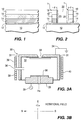
- Fig. 1 illustrates the initial sequence of layers used to form the present transistor gates.
- a gate oxide layer 12 is put down first over the substrate 10
- a polysilicon layer 14 is put down first over the substrate 10
- a tungsten silicide layer 16 and a photoresist layer 18 are sequentially deposited thereover.
- the gate structure is etched down to the silicon oxide layer 12.
- the resultant patterned gates 1 are shown in Fig. 2.
- the photoresist layer 18 is then removed or stripped in conventional manner.
- the gate structure of Fig. 2 have smooth, vertical sidewalls, with no undercutting either between the tungsten silicide and the polysilicon, or at the polysilicon- silicon oxide interface.
- a suitable conventional etchant is a mixture of SF 6 and HBr.
- photoresist has been found to be inadequate to maintain dimensional control during the etch.
- photoresist it has been found that some gate structures, particularly at the end of a row of gates, or for more isolated gate structures, the dimensional control is not acceptable and the sidewall profiles are non-uniform. This is known as microloading or profile microloading.
- a hardmask of silicon oxide is substituted for the photoresist.
- a silicon oxide layer is deposited over the tungsten silicide layer, followed by photoresist.
- the photoresist is patterned in conventional manner, and the oxide layer is selectively etched to form the hardmask. Good control of dimensions of the oxide hardmask layer can be obtained to form gates having a cross section below 0.5 micron, e.g., 0.25-0.35 micron.
- the photoresist layer is stripped and the patterned oxide layer is used as the masking layer to etch the gate layers.
- the resultant structure is the same as shown in Fig. 2, except that a hardmask layer is substituted for the photoresist layer 18.
- the etched sidewalls 20 should be straight with an opening 22 formed between them.
- the thickness of the gate oxide layer 12 is very important and varies with the gate length in accordance with the device design. However, for fast, smaller devices, the thickness of the gate oxide layer 12 is preferably on the order of 90 angstroms thick. If the gate oxide layer is too thick, the device speed is lowered. If the gate oxide layer is too thin, there is a danger of etching through this layer to the underlying substrate, shorting out the device.
- the gate oxide layer 12 is thin in comparison to the thickness of the gate layers, a high selectivity between the polysilicon layer 14 and the gate oxide layer 12 is required to avoid etching through the thin gate oxide layer 12.
- the transistor gates herein include a polysilicon layer 14 about 1000 ⁇ thick; a tungsten silicide layer 16 about 1500 ⁇ thick and a hardmask silicon oxide layer about 5000 ⁇ thick.
- silicon oxide hardmasks microloading is improved, selectivity is improved and the critical dimension is higher.
- etch composition comprising NF 3 and Cl 2 for etching transistor gates comprising tungsten silicide and polysilicon provides low microloading for the hard mask, high etch selectivity to the gate oxide and excellent profile control, as well as acceptable etch rates.
- the etchant composition preferably includes a sidewall passivant such as hydrogen bromide (HBr).
- HBr hydrogen bromide
- Other passivation materials such as nitrogen and/or oxygen can also be used.
- Fig. 1 is a cross sectional view of an unetched gate structure for a tungsten silicide-polysilicon gate.
- Fig. 2 is a cross sectional view of the gate structure of Fig. 1 after etching.
- Figs. 3A and 3B are a cross sectional view of an etch chamber in which the present etch process can be carried out.
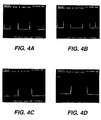
- Figs. 4A, 4B, 4C and 4D are photomicrographs of cross sectional views of gate structures etched using the etchant composition of the invention.
- Figs. 5A and 5B are photomicrographs of cross sectional views of gate structures etched using an etchant composition of the prior art.
- Figs. 6A and 6B are photomicrographs of cross sectional views of gate structures etched using an alternate etchant composition of the prior art.
- Figs. 7A and 7B are photomicrographs of cross sectional views of gate structures etching using still another alternate etchant composition of the prior art.
- Figs. 8A, 8B and 8C are photomicrographs of cross sectional views of gate structures etched in accordance with the invention at varying substrate temperatures.
- the optimal criteria desired for etching gate structures of the invention is a high etch rate for both polysilicon and tungsten silicide of about 2000-3000 angstroms per minute ( ⁇ /min), with a selectivity close to 1:1 between the tungsten silicide and the polysilicon layers, and a higher selectivity, i.e., about 5:1 selectivity between the polysilicon and the hardmask gate oxide layer; a wall profile angle of close to 90° with respect to the substrate; a variation in etch uniformity of 3% or less across the wafer; reduced microloading and minimal etching of the gate oxide layer.
- the present etch composition has a selectivity of tungsten silicide:polysilicon of 0.75:1, and a selectivity of polysilicon to the hardmask gate oxide of 2.8:1.
- the overall etch rate is about 2000 to 2200 ⁇ /min for tungsten silicide, and about 3000 ⁇ /min for polysilicon.
- the overetch rate for the present etch composition is high, 2500 ⁇ /min, the uniformity is good at about 5% and selectivity to the gate oxide is high at 85:1.
- the present etch process can be carried out advantageously in an etch chamber as shown in Fig. 3A.
- the chamber 30 includes walls 31 housing a reactor chamber 32. Processing gases are introduced to the chamber 32 via a nozzle 33. The nozzle 33 is connected to the walls 31 which are grounded via line 34.
- a cathode support electrode 35 supports the wafer 38 to be treated.
- the wafer 38 is passed into the chamber by means of a slit valve 36.
- the cathode support electrode 35 is connected to a source of power 39 and is also connected to an elevator mechanism (not shown) for raising and lowering the support 35 while the wafer 38 is moved into and out of the chamber.
- the wafer 38 can be cooled by passing a flow of helium to the backside of the wafer 38. Conventional clamps or fingers (not shown) connected to the support electrode 35 maintain the wafer 38 in alignment during processing.
- a suitable pressure is maintained in the chamber by an exhaust system (not shown).
- a plasma is formed from the processing gases in the region between the
- a pair of helmholtz configured electromagnetic coils 39, 40 provide a transverse magnetic field with the north and south poles at the left and right providing a horizontal magnetic field axis parallel to the surface of the wafer 38.
- the transverse magnetic field is applied to slow the vertical velocity of electrons in the plasma which are accelerated radially by the magnetic field as they move towards the wafer 38. Accordingly, the quantity of electrons in the plasma is increased by means of this transverse magnetic field and the plasma is enhanced.
- the potential drop across the cathode sheath can be decreased to increase the ion current flux present on the wafer surface, permitting higher rates of etching without requiring higher ion energies to achieve this result. As shown in Fig.
- the vector of the magnetic field rotates about the center axis of the electrical field by varying the phases of current flowing through the coils 39, 40 at a typical rotational frequency of 0.01 to 1 Hz, producing a variable strength of the magnetic flux, typically from 0-150 Gauss, determined by the current supplied to the coils.
- Suitable chambers are available commercially from Applied Materials, Inc as the MxP or MxP Plus chamber.
- the power to the chamber is generally set at 100-500 watts. If the power is too low, an inverse taper for the openings may be obtained, which is not desirable, particularly when the openings 22 are to be filled in.
- the pressure during etching is generally maintained at about 20 to 25 millitorr to maintain straight sidewalls of the etched profiles.
- the composition of the etchant of the invention preferably includes from 75 to 85% by volume of chlorine and from 15 to 25% by volume of NF 3 .
- the preferred etchant composition is 75 to 80% by volume of chlorine, 10 to 15% by volume of NF 3 and 5 to 10% by volume of HBr.
- the temperature of the substrate affects the sidewall taper and the etch rate
- the temperature of the substrate during etching is chosen depending on the sidewall taper and etch rate desired.
- a silicon wafer having a layer of gate oxide thereon about 90 ⁇ thick, a layer of polysilicon 1000 ⁇ thick thereover, a layer of tungsten silicide (WSi x ) 1500 ⁇ thick and a patterned silicon oxide hardmask layer thereover 1500 ⁇ thick was patterned as an array of openings having 0.3 micron dimensions, in an etch chamber as in Fig. 3. The pressure of the chamber was brought to 20 millitorr.
- a gas flow of 20 sccm of NF 3 , 15 sccm of HBr and 90 sccm of chlorine was passed into the chamber.
- the power was set at 500 watts, and the magnetic field at 30 gauss.
- the substrate temperature was 80°C. Etching was continued for 47 seconds for an etch rate of about 2200 ⁇ /min for the tungsten silicide.
- An overetch was carried out for 30 seconds using an etch composition of 50 sccm HBr, 10 sccm of chlorine and 3 sccm or a helium/oxygen mixture at 80 millitorr pressure, power of 150 watts, and magnetic field at 30 gauss.
- the etch rate was 2500 ⁇ /min, the etch rate uniformity was 5%, and the selectivity to the gate oxide was about 85:1.
- Figs. 4A, 4B, 4C and 4D is a series of cross sectional views of the resulting openings taken from the center (4A and 4B) and edge (4C and 4D) of the wafer. It is apparent that the openings had straight sidewalls with no undercutting.
- the etch rate was 2200 ⁇ /min and the etch rate uniformity across the wafer was 5.1%; the selectivity of WSi x to polysilicon was 0.75:1 and the selectivity to the gate oxide was 2.8:1; etch rate microloading was less than 3%; and the profile microloading variation was less than 1°; that is, the angle of the sidewall with respect to the substrate was found to be 89° for an opening at the center of the wafer, and 90° for an opening at the edge of the wafer. A slight faceting of the upper edge of the opening can be seen.
- Example 1 The procedure of Example 1 was followed except substituting as the gas flows 25 sccm of SF 6 and 35 sccm of chlorine. The pressure was held at 25 millitorr, the power was set at 275 watts, the magnetic field at 30 gauss, and the substrate temperature was 40°C. Etching was continued for 50 seconds.
- Example 1 An overetch was carried out as in Example 1.
- the overetch rate was 1250 ⁇ /min, the overetch uniformity was 3% and the selectivity of polysilicon to the gate oxide was about 100:1.
- the etch rate was 2400 ⁇ /min and the etch rate uniformity was 6-8%; microloading was 6-7%, and profile microloading was 5-7%.
- the angle between the sidewall and the substrate was 87° at the center of the wafer and 92° at the edge of the wafer. Also the sidewalls were more tapered than those formed in Example 1 as can be seen in Figs. 5A and 5B. Some undercutting is apparent.
- Example 1 The procedure of Example 1 was followed except substituting the following gas flows: 60 sccm SF 6 and 20 sccm HBr. The pressure was held at 20 millitorr, the power was set at 250 watts, the magnetic field at 30 gauss and the substrate temperature was 80°C. An overetch was carried out as in Example 1.
- etch rate uniformity was only 10-13%; etch rate microloading was 10-12%; and profile microloading was less than 1°.
- Figs. 6A and 6B some undercutting can be seen at the polysilicon to gate oxide interface. There is a marked taper to the etched profiles.
- Example 1 The procedure of Example 1 was followed etching 0.25 micron openings.
- the etchant mixture was 26 sccm of chlorine and 52 sccm of SF 6 .
- the chamber pressure was 25 millitorr, the power was set at 200 watts, and the magnetic field at 30 gauss.
- etched profiles are shown in Figs. 7A and 7B for the center and edge of the wafer respectively. Slightly tapered sidewalls were obtained.
- etch rate uniformity was 6-8%
- etch rate microloading was 5-7%
- profile microloading was 6-7%.
- This example shows the variation of profile control versus substrate temperature during etching.
- Example 1 The procedure of Example 1 was followed using etchant gas flows of 90 sccm chlorine, 10 sccm NF 3 and 15 sccm HBr. The etch was done at a chamber pressure of 20 millitorr, the power set at 450 watts, the magnetic field at 30 gauss and the temperature at 40°C. No overetch was carried out on these samples.
- Fig. 8A illustrates the profile obtained at 40°C.
- the sidewalls are somewhat tapered.
- the endpoint was reached in 87 seconds, with 14% of the polysilicon remaining.
- Fig. 8B illustrates the profile obtained at a 65°C substrate temperature.
- the sidewalls are less tapered than those of Fig. 8A and no undercutting was observed.
- the endpoint was reached in 64 seconds, with 11% of the polysilicon remaining. Thus etching was more complete and the etch rate was higher.
- Fig. 8C illustrates the profile obtained. Straight walled profiles were obtained with no undercutting.
Abstract
Description
Claims (10)
- An etch composition for etching transistor gates on a silicon oxide layer comprising a layer of tungsten silicide over a layer of polysilicon adjacent to said silicon oxide layer, using a silicon oxide hardmask, the etch composition comprising a mixture of nitrogen trifluoride and chlorine.
- An etch composition according to claim 1 additionally including one or more of hydrogen bromide, nitrogen, oxygen and a carrier gas.
- An etch composition according to claim 1 or claim 2 comprising from 75 to 85% by volume of chlorine and from 15 to 25% by volume of nitrogen trifluoride.
- An etch composition according to claim 1 or claim 2 comprising from 75% to 80% by volume of chlorine, 10 to 15% by volume of nitrogen trifluoride and 5 to 10% by volume of hydrogen bromide.
- A method of etching transistor gates comprising sequential layers of gate oxide, polysilicon and tungsten silicide on a substrate and using a patterned silicon oxide layer as a hardmask, the method comprising etching the tungsten silicide and polysilicon layers with an etchant composition including nitrogen trifluoride and chlorine.
- A method according to claim 5, wherein the etchant composition comprises from 75% to 85% by volume of chlorine and from 15 to 25% by volume of nitrogen trifluoride.
- A method according to claim 5 or claim 6, wherein said etchant composition further includes hydrogen bromide.
- A method according to claim 7, wherein the etchant composition comprises from 75% to 80 by volume of chlorine, 10 to 15% by volume of nitrogen trifluoride and 5 to 10% by volume of hydrogen bromide.
- A method according to any one of claim 6 to 8, wherein said tungsten silicide layer is about 1500 angstroms thick, said polysilicon layer is about 1000 angstroms thick and said gate oxide layer is from about 90 to 100 angstroms thick.
- A method according to any one of claims 6 to 9, wherein the temperature of etching is chosen to obtain the desired profile.
Applications Claiming Priority (2)
| Application Number | Priority Date | Filing Date | Title |
|---|---|---|---|
| US724383 | 1996-10-01 | ||
| US08/724,383 US5851926A (en) | 1996-10-01 | 1996-10-01 | Method for etching transistor gates using a hardmask |
Publications (2)
| Publication Number | Publication Date |
|---|---|
| EP0837497A2 true EP0837497A2 (en) | 1998-04-22 |
| EP0837497A3 EP0837497A3 (en) | 1998-06-10 |
Family
ID=24910219
Family Applications (1)
| Application Number | Title | Priority Date | Filing Date |
|---|---|---|---|
| EP97307549A Withdrawn EP0837497A3 (en) | 1996-10-01 | 1997-09-25 | Method for etching transistor gates using a hardmask |
Country Status (6)
| Country | Link |
|---|---|
| US (1) | US5851926A (en) |
| EP (1) | EP0837497A3 (en) |
| JP (1) | JPH10135194A (en) |
| KR (1) | KR19980032466A (en) |
| SG (1) | SG67421A1 (en) |
| TW (1) | TW360921B (en) |
Cited By (8)
| Publication number | Priority date | Publication date | Assignee | Title |
|---|---|---|---|---|
| WO2000044037A1 (en) * | 1999-01-22 | 2000-07-27 | Advanced Micro Devices, Inc. | Method of in-situ etching a hard mask and a metal layer in a single etcher |
| WO2001061740A1 (en) * | 2000-02-18 | 2001-08-23 | Applied Materials, Inc. | Self-cleaning process for etching silicon-containing material |
| US6322714B1 (en) | 1997-11-12 | 2001-11-27 | Applied Materials Inc. | Process for etching silicon-containing material on substrates |
| US6797188B1 (en) | 1997-11-12 | 2004-09-28 | Meihua Shen | Self-cleaning process for etching silicon-containing material |
| US6872322B1 (en) | 1997-11-12 | 2005-03-29 | Applied Materials, Inc. | Multiple stage process for cleaning process chambers |
| DE10358025A1 (en) * | 2003-12-11 | 2005-07-21 | Infineon Technologies Ag | Etching of tungsten involves using a gas mixture that contains nitrogen trifluoride, hydrogen bromide, and oxygen |
| WO2006130744A1 (en) * | 2005-06-01 | 2006-12-07 | Lam Research Corporation | Tungsten silicide etch process with reduced etch rate micro-loading |
| US7192532B2 (en) | 2001-04-19 | 2007-03-20 | Tokyo Electron Limited | Dry etching method |
Families Citing this family (17)
| Publication number | Priority date | Publication date | Assignee | Title |
|---|---|---|---|---|
| US6074956A (en) * | 1998-05-12 | 2000-06-13 | Advanced Micro Devices, Inc. | Method for preventing silicide residue formation in a semiconductor device |
| US6303513B1 (en) | 1999-06-07 | 2001-10-16 | Applied Materials, Inc. | Method for controlling a profile of a structure formed on a substrate |
| US6402974B1 (en) | 1999-07-27 | 2002-06-11 | Applied Materials, Inc. | Method for etching polysilicon to have a smooth surface |
| US6174818B1 (en) * | 1999-11-19 | 2001-01-16 | Taiwan Semiconductor Manufacturing Company | Method of patterning narrow gate electrode |
| US6544887B1 (en) | 2000-03-31 | 2003-04-08 | Lam Research Corporation | Polycide etch process |
| US6551942B2 (en) | 2001-06-15 | 2003-04-22 | International Business Machines Corporation | Methods for etching tungsten stack structures |
| US20070066076A1 (en) * | 2005-09-19 | 2007-03-22 | Bailey Joel B | Substrate processing method and apparatus using a combustion flame |
| US7202170B2 (en) * | 2004-01-20 | 2007-04-10 | Taiwan Semiconductor Manufacturing Co., Ltd. | Method of improving etching profile of floating gates for flash memory devices |
| US7060628B2 (en) * | 2004-03-19 | 2006-06-13 | Taiwan Semiconductor Manufacturing Co., Ltd. | Method for fabricating a hard mask polysilicon gate |
| TWI319204B (en) * | 2004-10-12 | 2010-01-01 | Hynix Semiconductor Inc | Method for fabricating semiconductor device using tungsten as sacrificial hard mask |
| KR20070003021A (en) * | 2005-06-30 | 2007-01-05 | 주식회사 하이닉스반도체 | Method for manufacturing semiconductor device |
| US7550381B2 (en) * | 2005-07-18 | 2009-06-23 | Applied Materials, Inc. | Contact clean by remote plasma and repair of silicide surface |
| US20070161246A1 (en) * | 2006-01-10 | 2007-07-12 | Texas Instruments Incorporated | Process For Selectively Removing Dielectric Material in the Presence of Metal Silicide |
| US20070184657A1 (en) * | 2006-02-09 | 2007-08-09 | Tokyo Electron Limited | Etching method |
| US8118946B2 (en) | 2007-11-30 | 2012-02-21 | Wesley George Lau | Cleaning process residues from substrate processing chamber components |
| JP5915027B2 (en) * | 2011-08-29 | 2016-05-11 | 大日本印刷株式会社 | Pattern forming structure and fine pattern forming method |
| US9385003B1 (en) * | 2015-02-16 | 2016-07-05 | Lam Research Corporation | Residue free systems and methods for isotropically etching silicon in tight spaces |
Citations (5)
| Publication number | Priority date | Publication date | Assignee | Title |
|---|---|---|---|---|
| US5228950A (en) * | 1990-12-04 | 1993-07-20 | Applied Materials, Inc. | Dry process for removal of undesirable oxide and/or silicon residues from semiconductor wafer after processing |
| US5346586A (en) * | 1992-12-23 | 1994-09-13 | Micron Semiconductor, Inc. | Method for selectively etching polysilicon to gate oxide using an insitu ozone photoresist strip |
| US5358601A (en) * | 1991-09-24 | 1994-10-25 | Micron Technology, Inc. | Process for isotropically etching semiconductor devices |
| EP0665579A1 (en) * | 1994-01-03 | 1995-08-02 | AT&T Corp. | Method of fabricating gate stack having a reduced height |
| US5605601A (en) * | 1995-09-19 | 1997-02-25 | Mitsubishi Denki Kabushiki Kaisha | Method of manufacturing semiconductor device |
Family Cites Families (2)
| Publication number | Priority date | Publication date | Assignee | Title |
|---|---|---|---|---|
| US5188704A (en) * | 1989-10-20 | 1993-02-23 | International Business Machines Corporation | Selective silicon nitride plasma etching |
| US5431772A (en) * | 1991-05-09 | 1995-07-11 | International Business Machines Corporation | Selective silicon nitride plasma etching process |
-
1996
- 1996-10-01 US US08/724,383 patent/US5851926A/en not_active Expired - Fee Related
-
1997
- 1997-09-25 EP EP97307549A patent/EP0837497A3/en not_active Withdrawn
- 1997-09-26 SG SG1997003582A patent/SG67421A1/en unknown
- 1997-09-30 TW TW086114219A patent/TW360921B/en active
- 1997-10-01 KR KR1019970050758A patent/KR19980032466A/en not_active Application Discontinuation
- 1997-10-01 JP JP9284693A patent/JPH10135194A/en not_active Withdrawn
Patent Citations (5)
| Publication number | Priority date | Publication date | Assignee | Title |
|---|---|---|---|---|
| US5228950A (en) * | 1990-12-04 | 1993-07-20 | Applied Materials, Inc. | Dry process for removal of undesirable oxide and/or silicon residues from semiconductor wafer after processing |
| US5358601A (en) * | 1991-09-24 | 1994-10-25 | Micron Technology, Inc. | Process for isotropically etching semiconductor devices |
| US5346586A (en) * | 1992-12-23 | 1994-09-13 | Micron Semiconductor, Inc. | Method for selectively etching polysilicon to gate oxide using an insitu ozone photoresist strip |
| EP0665579A1 (en) * | 1994-01-03 | 1995-08-02 | AT&T Corp. | Method of fabricating gate stack having a reduced height |
| US5605601A (en) * | 1995-09-19 | 1997-02-25 | Mitsubishi Denki Kabushiki Kaisha | Method of manufacturing semiconductor device |
Cited By (13)
| Publication number | Priority date | Publication date | Assignee | Title |
|---|---|---|---|---|
| US6322714B1 (en) | 1997-11-12 | 2001-11-27 | Applied Materials Inc. | Process for etching silicon-containing material on substrates |
| US6797188B1 (en) | 1997-11-12 | 2004-09-28 | Meihua Shen | Self-cleaning process for etching silicon-containing material |
| US6872322B1 (en) | 1997-11-12 | 2005-03-29 | Applied Materials, Inc. | Multiple stage process for cleaning process chambers |
| WO2000044037A1 (en) * | 1999-01-22 | 2000-07-27 | Advanced Micro Devices, Inc. | Method of in-situ etching a hard mask and a metal layer in a single etcher |
| US6159863A (en) * | 1999-01-22 | 2000-12-12 | Advanced Micro Devices, Inc. | Insitu hardmask and metal etch in a single etcher |
| KR100708422B1 (en) * | 1999-01-22 | 2007-04-18 | 어드밴스드 마이크로 디바이시즈, 인코포레이티드 | Method of in-situ etching a hard mask and a metal layer in a single etcher |
| WO2001061740A1 (en) * | 2000-02-18 | 2001-08-23 | Applied Materials, Inc. | Self-cleaning process for etching silicon-containing material |
| CN1310293C (en) * | 2001-04-19 | 2007-04-11 | 东京毅力科创株式会社 | Dry etching method |
| US7192532B2 (en) | 2001-04-19 | 2007-03-20 | Tokyo Electron Limited | Dry etching method |
| DE10358025A1 (en) * | 2003-12-11 | 2005-07-21 | Infineon Technologies Ag | Etching of tungsten involves using a gas mixture that contains nitrogen trifluoride, hydrogen bromide, and oxygen |
| WO2006130744A1 (en) * | 2005-06-01 | 2006-12-07 | Lam Research Corporation | Tungsten silicide etch process with reduced etch rate micro-loading |
| US7413992B2 (en) | 2005-06-01 | 2008-08-19 | Lam Research Corporation | Tungsten silicide etch process with reduced etch rate micro-loading |
| CN101189709B (en) * | 2005-06-01 | 2010-04-14 | 朗姆研究公司 | Tungsten silicide etch process with reduced etch rate micro-loading |
Also Published As
| Publication number | Publication date |
|---|---|
| EP0837497A3 (en) | 1998-06-10 |
| TW360921B (en) | 1999-06-11 |
| US5851926A (en) | 1998-12-22 |
| SG67421A1 (en) | 1999-09-21 |
| JPH10135194A (en) | 1998-05-22 |
| KR19980032466A (en) | 1998-07-25 |
Similar Documents
| Publication | Publication Date | Title |
|---|---|---|
| US5851926A (en) | Method for etching transistor gates using a hardmask | |
| US5007982A (en) | Reactive ion etching of silicon with hydrogen bromide | |
| EP0167136B1 (en) | Selective anisotropic reactive ion etching process for polysilicide composite structures | |
| EP0049272B1 (en) | Fabrication of microminiature devices using plasma etching of silicon with fluorine-containing gaseous compounds | |
| US5094712A (en) | One chamber in-situ etch process for oxide and conductive material | |
| US5942446A (en) | Fluorocarbon polymer layer deposition predominant pre-etch plasma etch method for forming patterned silicon containing dielectric layer | |
| EP0314990B1 (en) | Process for preferentially etching polycrystalline silicon | |
| US6569773B1 (en) | Method for anisotropic plasma-chemical dry etching of silicon nitride layers using a gas mixture containing fluorine | |
| US5431772A (en) | Selective silicon nitride plasma etching process | |
| US5256245A (en) | Use of a clean up step to form more vertical profiles of polycrystalline silicon sidewalls during the manufacture of a semiconductor device | |
| US6037265A (en) | Etchant gas and a method for etching transistor gates | |
| US6008139A (en) | Method of etching polycide structures | |
| US4264409A (en) | Contamination-free selective reactive ion etching or polycrystalline silicon against silicon dioxide | |
| US20020164885A1 (en) | Method of making small transistor lengths | |
| JPH06163478A (en) | Dry etching method of semiconductor | |
| KR20020027520A (en) | Sidewall polymer forming gas additives for etching processes | |
| US20060011579A1 (en) | Gas compositions | |
| US5880033A (en) | Method for etching metal silicide with high selectivity to polysilicon | |
| JPS6365625A (en) | Etching | |
| WO1999016110A2 (en) | Plasma process for selectively etching oxide using fluoropropane or fluoropropylene | |
| US5871659A (en) | Dry etching process for semiconductor | |
| JPH06163481A (en) | Dry etching method of semiconductor | |
| US4479850A (en) | Method for etching integrated semiconductor circuits containing double layers consisting of polysilicon and metal silicide | |
| US6461969B1 (en) | Multiple-step plasma etching process for silicon nitride | |
| JPH06338479A (en) | Etching method |
Legal Events
| Date | Code | Title | Description |
|---|---|---|---|
| PUAI | Public reference made under article 153(3) epc to a published international application that has entered the european phase |
Free format text: ORIGINAL CODE: 0009012 |
|
| AK | Designated contracting states |
Kind code of ref document: A2 Designated state(s): AT BE CH |
|
| AX | Request for extension of the european patent |
Free format text: AL;LT;LV;RO;SI |
|
| PUAL | Search report despatched |
Free format text: ORIGINAL CODE: 0009013 |
|
| RIN1 | Information on inventor provided before grant (corrected) |
Inventor name: WILTSE, MARK Inventor name: MINAEE, BRUCE Inventor name: GUENTER, ROLF ADOLF Inventor name: JIANG, WEINAN Inventor name: DESHMUKH, SHASHANK C. Inventor name: CHINN, JEFFREY Inventor name: KUMAR, AJAY |
|
| AK | Designated contracting states |
Kind code of ref document: A3 Designated state(s): AT BE CH DE DK ES FI FR GB GR IE IT LI LU MC NL PT SE |
|
| AX | Request for extension of the european patent |
Free format text: AL;LT;LV;RO;SI |
|
| 17P | Request for examination filed |
Effective date: 19981209 |
|
| AKX | Designation fees paid |
Free format text: DE FR GB |
|
| RBV | Designated contracting states (corrected) |
Designated state(s): DE FR GB |
|
| STAA | Information on the status of an ep patent application or granted ep patent |
Free format text: STATUS: THE APPLICATION HAS BEEN WITHDRAWN |
|
| 18W | Application withdrawn |
Withdrawal date: 19990810 |