EP0829188B1 - Contact arrangement for detachably attaching an electric component, especially an integrated circuit to a printed circuit board - Google Patents
Contact arrangement for detachably attaching an electric component, especially an integrated circuit to a printed circuit board Download PDFInfo
- Publication number
- EP0829188B1 EP0829188B1 EP96919752A EP96919752A EP0829188B1 EP 0829188 B1 EP0829188 B1 EP 0829188B1 EP 96919752 A EP96919752 A EP 96919752A EP 96919752 A EP96919752 A EP 96919752A EP 0829188 B1 EP0829188 B1 EP 0829188B1
- Authority
- EP
- European Patent Office
- Prior art keywords
- contact
- arrangement according
- printed circuit
- contact arrangement
- circuit board
- Prior art date
- Legal status (The legal status is an assumption and is not a legal conclusion. Google has not performed a legal analysis and makes no representation as to the accuracy of the status listed.)
- Expired - Lifetime
Links
- 238000003825 pressing Methods 0.000 claims description 11
- 239000004020 conductor Substances 0.000 claims description 9
- 239000000463 material Substances 0.000 claims description 4
- 229920002994 synthetic fiber Polymers 0.000 claims description 4
- 239000004593 Epoxy Substances 0.000 claims description 3
- 229920001169 thermoplastic Polymers 0.000 claims description 3
- 239000004416 thermosoftening plastic Substances 0.000 claims description 3
- 230000000284 resting effect Effects 0.000 claims 1
- 238000001816 cooling Methods 0.000 description 8
- 239000002184 metal Substances 0.000 description 7
- 238000013461 design Methods 0.000 description 4
- 238000000034 method Methods 0.000 description 4
- 230000000694 effects Effects 0.000 description 3
- 238000005516 engineering process Methods 0.000 description 3
- 229920002379 silicone rubber Polymers 0.000 description 3
- 239000004945 silicone rubber Substances 0.000 description 3
- 229910001111 Fine metal Inorganic materials 0.000 description 2
- 238000010276 construction Methods 0.000 description 2
- 230000006378 damage Effects 0.000 description 2
- 238000003780 insertion Methods 0.000 description 2
- 230000037431 insertion Effects 0.000 description 2
- 239000004033 plastic Substances 0.000 description 2
- 238000007747 plating Methods 0.000 description 2
- 125000006850 spacer group Chemical group 0.000 description 2
- 230000000712 assembly Effects 0.000 description 1
- 238000000429 assembly Methods 0.000 description 1
- 238000005452 bending Methods 0.000 description 1
- 230000005540 biological transmission Effects 0.000 description 1
- 230000015572 biosynthetic process Effects 0.000 description 1
- 239000011248 coating agent Substances 0.000 description 1
- 238000000576 coating method Methods 0.000 description 1
- 238000011161 development Methods 0.000 description 1
- 230000018109 developmental process Effects 0.000 description 1
- 239000012777 electrically insulating material Substances 0.000 description 1
- 238000009713 electroplating Methods 0.000 description 1
- 238000004519 manufacturing process Methods 0.000 description 1
- 230000035515 penetration Effects 0.000 description 1
- 238000010079 rubber tapping Methods 0.000 description 1
- 229910000679 solder Inorganic materials 0.000 description 1
- 238000012360 testing method Methods 0.000 description 1
Images



Classifications
-
- H—ELECTRICITY
- H01—ELECTRIC ELEMENTS
- H01R—ELECTRICALLY-CONDUCTIVE CONNECTIONS; STRUCTURAL ASSOCIATIONS OF A PLURALITY OF MUTUALLY-INSULATED ELECTRICAL CONNECTING ELEMENTS; COUPLING DEVICES; CURRENT COLLECTORS
- H01R13/00—Details of coupling devices of the kinds covered by groups H01R12/70 or H01R24/00 - H01R33/00
- H01R13/02—Contact members
- H01R13/22—Contacts for co-operating by abutting
- H01R13/24—Contacts for co-operating by abutting resilient; resiliently-mounted
- H01R13/2464—Contacts for co-operating by abutting resilient; resiliently-mounted characterized by the contact point
-
- H—ELECTRICITY
- H05—ELECTRIC TECHNIQUES NOT OTHERWISE PROVIDED FOR
- H05K—PRINTED CIRCUITS; CASINGS OR CONSTRUCTIONAL DETAILS OF ELECTRIC APPARATUS; MANUFACTURE OF ASSEMBLAGES OF ELECTRICAL COMPONENTS
- H05K7/00—Constructional details common to different types of electric apparatus
- H05K7/02—Arrangements of circuit components or wiring on supporting structure
- H05K7/10—Plug-in assemblages of components, e.g. IC sockets
-
- H—ELECTRICITY
- H01—ELECTRIC ELEMENTS
- H01R—ELECTRICALLY-CONDUCTIVE CONNECTIONS; STRUCTURAL ASSOCIATIONS OF A PLURALITY OF MUTUALLY-INSULATED ELECTRICAL CONNECTING ELEMENTS; COUPLING DEVICES; CURRENT COLLECTORS
- H01R13/00—Details of coupling devices of the kinds covered by groups H01R12/70 or H01R24/00 - H01R33/00
- H01R13/02—Contact members
- H01R13/22—Contacts for co-operating by abutting
- H01R13/24—Contacts for co-operating by abutting resilient; resiliently-mounted
- H01R13/2464—Contacts for co-operating by abutting resilient; resiliently-mounted characterized by the contact point
- H01R13/2471—Contacts for co-operating by abutting resilient; resiliently-mounted characterized by the contact point pin shaped
-
- H—ELECTRICITY
- H01—ELECTRIC ELEMENTS
- H01R—ELECTRICALLY-CONDUCTIVE CONNECTIONS; STRUCTURAL ASSOCIATIONS OF A PLURALITY OF MUTUALLY-INSULATED ELECTRICAL CONNECTING ELEMENTS; COUPLING DEVICES; CURRENT COLLECTORS
- H01R13/00—Details of coupling devices of the kinds covered by groups H01R12/70 or H01R24/00 - H01R33/00
- H01R13/02—Contact members
- H01R13/22—Contacts for co-operating by abutting
- H01R13/24—Contacts for co-operating by abutting resilient; resiliently-mounted
- H01R13/2464—Contacts for co-operating by abutting resilient; resiliently-mounted characterized by the contact point
- H01R13/2492—Contacts for co-operating by abutting resilient; resiliently-mounted characterized by the contact point multiple contact points
-
- H—ELECTRICITY
- H05—ELECTRIC TECHNIQUES NOT OTHERWISE PROVIDED FOR
- H05K—PRINTED CIRCUITS; CASINGS OR CONSTRUCTIONAL DETAILS OF ELECTRIC APPARATUS; MANUFACTURE OF ASSEMBLAGES OF ELECTRICAL COMPONENTS
- H05K7/00—Constructional details common to different types of electric apparatus
- H05K7/02—Arrangements of circuit components or wiring on supporting structure
- H05K7/10—Plug-in assemblages of components, e.g. IC sockets
- H05K7/1053—Plug-in assemblages of components, e.g. IC sockets having interior leads
- H05K7/1061—Plug-in assemblages of components, e.g. IC sockets having interior leads co-operating by abutting
- H05K7/1069—Plug-in assemblages of components, e.g. IC sockets having interior leads co-operating by abutting with spring contact pieces
Definitions
- the present invention relates to a contact arrangement for detachably attaching an electrical component having a plurality of terminal contacts, for example an integrated circuit of the BGA-type (ball grid array), of the CGA-type (column grid array), of the LGA-type (land grid array) or of the flip-chip type, to a printed circuit board, having a number of electrically conductive contact pins which are directly attachable to the printed circuit board and in attached state extend away from the printed circuit board at about right angles, each of the contact pins being connected to at least one conductor path of the printed circuit board for establishing an electrical connection.
- the present invention further relates to the board-to-board connexion between two printed circuit boards.
- Such LSI circuits may also be considerably expensive.
- Connector blocks have therefore been created which are soldered to the conductor paths of a printed circuit board instead of the integrated circuit.
- a connector block has contact arrangements formed in such a way that an integrated circuit can be pluggably connected to the connector block. In this way, the highly complex integrated circuit is exchangeable at any time.
- Such integrated circuits can be plugged into a frame-shaped connector block. There, there is a spring contact-lug for each terminal of the integrated circuit.
- This kind of connector block is provided for the mounting of integrated circuits corresponding to the PLCC construction form.
- PGA pin grid array
- Connector blocks for these provide contact pins disposed in a plastic slab corresponding to the grid of the terminal pins of the integrated circuit.
- the contact pins are essentially formed as jacks which on one side can be plugged into a hole mask on the printed circuit board and soldered to the conductor paths there and on the other side have contact springs inside each jack for ensuring a faultless electrical contact with the contact pin to be received.
- the design of the LSI circuits has likewise been adapted to the art of surface mounting technology (SMT).
- SMT surface mounting technology
- the terminals of an integrated circuit disposed in a grid array have no longer been made pin-shaped but substantially spherical-segment-shaped.
- a pin there protrudes from the underside of the housing of the integrated circuit for each terminal a spherical segment, preferably, say, a hemisphere.
- the terminal arrangement of thus integrated circuits is known by the term ball grid array (BGA).
- BGA ball grid array
- the dome-shaped terminals of such integrated circuits, during attachment of the latter to a printed circuit board, are soldered directly to contact areas of the printed circuit board.
- reliable contact-making is to be ensured for every terminal, even with an extremely great number of terminals, and nonetheless the force to be expended for inserting or removing the integrated circuit is to be so little that, in any case, destruction of the integrated circuit through too great actions of force can be excluded.
- EP-A-360 485 dicloses a package for pin grid array integrated circuits.
- Patent document US-A-4 922 376 discloses contact arrangements comprising an axially compressible, electrically conductive contact element for establishing an electrical connection between a contact pin of a circuit board and the terminal pin of a plurality of intergrated circuits.
- the contacts pins are inserted in bores in a support. No space is provided in the bores for guiding and aligning the terminal pins.
- this task is solved with a contact arrangement as defined in claim 1 for detachably attaching an electrical component having a plurality terminal contacts to a printed circuit board, comprising a support disposable between said electrical component and said printed circuit board and comprising a plurality of bores arranged in the same way as said terminal contacts, a number of electrically conductive contact pins which are directly attachable to the printed circuit board and in attached state extend away from the printed circuit board at about right angles, each of the contact pins being disposed in one of said bores and being connectable to at least one conductor path of the printed circuit board for establishing an electrical connection, the contact pins are made in one piece, a space extending away in each of said bore from the free end of the contact pin between each contact pin and a therewith associated terminal contact of an electrical component when said electrical component is attached on said contact arrangement, and the space is bridged by an axially compressible, electrically conductive contact element for establishing an electrical connection between the contact pin and the terminal contact of the electrical component.
- This task is furthermore solved
- the force necessary for inserting the integrated circuit in the contact arrangement according to the invention is determined merely according to the number of terminal contacts and the force necessary for compressing the contact element which extends away from each contact pin end. This force is relatively slight as compared with that necessary for inserting integrated circuits having terminal pins in a corresponding connector block. It has turned out that contact- making is faultless even when the underside of the housing of the integrated circuit is not absolute plane or not all the dome-shaped terminal contacts are identically formed and protrude the same distance from the underside of the integrated circuit. This may very well be the case, for example after tin-plating of the terminal contacts.
- an integrated circuit is preferably intended as an electrical component.
- the invention shall not be limited thereto but rather also be accessible to other electrical components having a similar terminal contact arrangement, if any.
- the present invention applies in particular to components, the terminal contacts of which are disposed in a ball grid array (BGA), in a column grid array (CGA), in a land grid array (LGA).
- BGA ball grid array
- CGA column grid array
- LGA land grid array
- the inventive idea further extends to flip-chips or to the interconnection between two printed circuit boards.
- the compressible, electrically conductive contact element is preferably a coil spring, one coil spring being provided per contact pin.
- This spring can be fastened to the contact pin in a relatively simple manner in that an extension is turned on the end of the latter, over which the contact spring can be pressed on. Then, in an electroplating process, the contact pin and the coil spring together can be coppered and thereafter tinned, for example. The coil spring then remains held on the end of the contact pin after this operation through the additional metal coating.
- a further preferred embodiment provides using for the compressible, electrically conductive contact element a rubber- elastic mat in which fine, gold-plated metal wires are embedded spaced close together.
- the rubber-elastic mat may be made of a silicone rubber. Such mats are commercially available and may be procured, for example, through the Japanese firm SHIN-ETSU. The thickness of these mats is between 0.3 and 1 mm, and the mutual spacing of the metal wires which penetrate the thickness of the mat, and are cut off about plane with the mat faces on both sides, amounts to 0.05 to 0.1 mm.
- the mat for the present application be cut to size in such a way that it corresponds at least to the lateral dimensions or to the shape of the underside of the housing of the electrical component and thus covers all terminal contacts of the latter.
- the ends of the contact pins over which the mat is placed are fashioned in such a way that several of the fine metal wires are contacted by the front face of the contact pin. It has turned out that for this purpose, the end of the contact pin is preferably made slightly dished, with an annular, not sharp; edged dish rim, or designed approximately as a crown-shaped structure comprising several non-sharp-edged teeth.
- the ends of the contact pins are also possible. It would be conceivable, for example, to combine these. In this way it may be ensured that through several, but at least through one metal wire, contact-making is reliably produced between the end of the contact pin and the terminal contact of the electrical component which lies on the side of the mat remote from the contact pins.
- a preferred embodiment further provides that the contact pins of the contact arrangement may be disposed in a plate-shaped support part which may be made of an epoxy material or of a thermoplastic synthetic material.
- the contact pins are inserted in bores of the plate-shaped support part, some of the contact pins facing the printed circuit board projecting from the support part and being formed for one of the known connection techniques with the printed circuit board, for example as a solder pin, or for SMD assembly.
- the end of the contact pins facing the electrical component does not project from the plate-shaped support part but ends in the bore, set back relative to the surface of the support part. It is thereby achieved that the uppermost region of each bore in the support part made of an electrically insulating material serves as a guide for the associated terminal contact of the electrical component.
- the terminal contacts can penetrate deeper or less deep. It may be provided that the terminal contacts can penetrate into the bores so far that the underside of the component rests on the top of the support part.
- the said spacing between the contact pins and the terminal contacts is always present, however, independently of the penetration depth. Reliable contact-making of the terminal contacts of the electrical component with the contact pins via the compressible contact elements does not take place until the electrical component to be put on has been correctly centered and then pressed down. Incorrect or slanting insertion is avoided by the guiding effect of the bore ends.
- the support part is divided into two superimposed plates, the rubber-elastic mat being disposed between the two plates.
- the contact pins are contained in the bores of one plate and substantially project just barely beyond the surface facing the other plate.
- the bores of the other plate are empty and serve as guides for the dome-shaped terminal contacts of the electrical component.
- the two plates of the support part with the compressible mat lying between them are, for example, screwed together, riveted, or joined to one another in some other common way.
- the contact pins be pressed into the bores. They are thereby held securely in the latter.
- the contact arrangement according to the invention likewise includes a holding-down device for pressing the terminal contacts of the electrical component down on the coil springs or the rubber-elastic mat.
- the holding-down device is made removable from the contact arrangement and is placed on the contact arrangement after the electrical component is put in place and produces on the top of the housing of the electrical component a force directed substantially perpendicular to the printed circuit board.
- the compressible electrical contact elements, the coil springs or the rubber-elastic mat with the fine metal wires, are thereby compressed between the terminal contacts of the electrical component and the contact pins opposite them, and the electric contact-making between the terminal contacts and the contact pins is produced.
- the holding-down device may be formed either as a spring which, when inserted, presses on the electrical component, or it may comprise non-spring holding-down elements which may be screwed onto the printed circuit board or the support part, in which case a tab present on each holding-down element presses on the top of the component.
- an adjustment means in the pressing-down tab for example a setscrew, by which the force acting on the top of the electrical component can be adjusted.
- the holding-down device may additionally also be formed in such a way that it comprises additional guide means for guiding the electrical component along its lateral faces.
- the contact arrangement By means of the design hit upon, it is possible to make the contact arrangement very small.
- the distance from one edge of the support part to the nearest contact pin is at most 5.2 mm.
- the overall height of the connector block formed by the support part with the inserted contact pins likewise amounts merely to 4.1 mm at most.
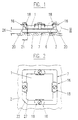
- a first exemplary embodiment of a contact arrangement is shown.
- 1 designates an electrical component, especially an integrated circuit, having terminal contacts 6 on its lower side, i.e. on the side facing a printed circuit board 2.
- the terminal contacts are distributed in a grid, substantially over the entire lower face of the electrical component. They are disposed in a network grid (grid array).
- Each terminal contact 6 has substantially the shape of a spherical segment, especially the shape of half a sphere, which stands out from the lower surface of the electrical component 1.
- the arrangement and shape of the terminal contacts is known by the name ball grid array (BGA).
- terminal contacts be distributed over the entire lower side of the housing of the electrical component or not.
- the terminal contacts would merely form a wreath, in which case there would be a contact-free area in the center of the integrated circuit.
- each contact pin 3 is inserted in a bore 13 which goes through a plate-shaped support part 7 along its thickness.
- the contact pins are pressed into the bores 13 from one side of the plate-shaped support part 7, the pressing-in path being limited by a stop ring 30 disposed encircling each contact pin 3.
- Each contact pin 3 has in addition about halfway along its length an encircling, slightly protruding collar 31 having a slightly sloping outer surface. This collar serves to reinforce the press fit of the contact pin 3 in the bore 13.
- one end of the contact pins 3 is formed substantially as a cylindrical journal having an approximately plane end face. This is provided for being soldered fast to the surface of a contact point 8, especially a conductor path of the printed circuit board 2. This process has become known by the term surface mounting.
- the parts mounted in this way are generally called SMD (surface-mounted device) parts.
- the contact pins 3 on the side facing the printed circuit board 2 protrude from the support part 7, on the other side of the support part 7 facing the electrical component 1 they are disposed set back in the bores 13.
- the end region 14 of each bore 13 thereby not penetrated by the contact pins 3 serves as a guide means for the terminal contacts 6 of the electrical component, or the integrated circuit 1, for positioning the latter relative to the entirety of the contact pins 3 forming the contact arrangement.
- the diameter of the end region 14 of the bore 13 can thereby be slightly smaller or slightly larger than the diameter of the terminal contact 6.
- the contact pins 3 extend in the soldered state approximately at right angles from the printed circuit board 2.
- the electrical component 1 is now placed on the plate-shaped support part 7 in such a way that its terminal contacts 6 project from above into the end regions 14 of the bores 13. There is then a space between the bottom end of each terminal contact 6 and the top of the associated contact pin 3. This space is designated by the reference numeral 9 (Fig. 4).
- the coil spring 4 Prior to the insertion in a bore 13 of a contact pin 3, the coil spring 4 been placed on the latter as described in the introduction of the description.
- each contact pin 3 has an appropriately shaped extension 11 at the end remote from the printed circuit board 2.
- the coil springs 4 are slightly compressed by the pressing of the terminal contacts of the electrical component 1 into the guide region 14 of the bores 13 and ensure faultless electrical connections between one terminal contact 6 and one contact pin 3 each, i.e., the respective contact area 8 of the printed circuit board 2. With the electrical component 1 removed, the free ends of the coil springs 4 are about flush with the surface of the plate-shaped support part 7. Even when the terminal contacts 6 are not carried out uniformly but protrude at varying distances from the underside of the electrical component, which may easily be the case through the tin-plating of the terminal contacts 6, a faultless electrical connection is ensured by the present design. Since no axial frictional forces act, the force for pressing the electrical component 1 into the guide openings 14 of the bores 13 is also possible with a reasonable expenditure of force which is in any case so small that no destruction of an integrated circuit 1 can be brought about thereby.
- the holding-down device 16 comprises four holding-down elements 18, one holding-down element 18 being disposed about halfway along each side of the approximately square-formed integrated circuit.
- Each holding-down element 18 comprises a fastening screw 23 screwed into a not specially depicted bore of the support part 7.
- the fastening screw 23 passes through a spacer 24, one end face of which rests on the support part 7 and the other end face of which rests against a guiding or holding- down tab 25 which is clamped between the last-mentioned end face and the screw head of the fastening screw 23.
- the guiding and holding- down tab extends with one leg 17, the end of which is bent down, over the edge area of the top of the housing of the integrated circuit 1. With fastening screw 23 screwed tight, the bent-down end of the said tab is intended as pressure means 17 to press the electrical component 1 down on the support part 7.
- the integrated circuit 1 is uniformly pressed down from above about halfway along each one of its longitudinal sides onto the plate-shaped support part 7. Uniform contact- making of all terminal contacts 6 with the associated contact pins 3 is achieved in this way.
- Each guiding and holding-down tab 25 further has guide means 15 which, in the exemplary embodiment shown, are formed as guide tabs bent down at right angles facing the support part 7.
- the guide tabs serve, besides the guide area 14 for the terminal contacts 6, to keep the electrical component 1 additionally guided on the support part 7.
- the fastening screws 23 may be formed self-tapping, they may be cylinder-head screws which engage a thread of the support part 7, this thread also being reinforceable by a threaded bushing, for example of metal, inserted in the support part 7. It would be conceivable, too, that the fastening screws 23 are not screwed tight on the support part 7 but that they merely traverse the latter and co-operate analogously with a thread existing in the printed circuit board 2.
- a single holding-down frame could be also foreseen, in accordance with Fig. 11, the inner frame edges lying on the upper surface of the electrical component 1 and pressing down thereon.
- This frame can be made of metal or preferably of a synthetic material.
- an additional lateral guide for the electrical component 1 to the end regions 14 of the bores 13 can be achieved through a further frame 36 supported on support part 7. This leads to an initial positioning of the electrical component 1 when the electrical component 1 is placed on support part 7.
- On the outside further frame 36 is preferably flush with support part 7. The area enclosed by the further frame 36 leaves open all end regions 14 of the bores 13.
- further frame 36 is pinched between support part 7 and the lower side of electrical component 1, and is thus held on the support part.
- Foreseen in further frame 36 are bores 37, which are congruent with bores 38 in holding-down frame 35.
- Led through these bores 37, 38 are fastening screws or respectively holding-down screws 39, which project into threaded linings 39 which have been put into support part 7.
- Achieved by means of the two frames 35, 36 is that the electrical component 1 in the area of its terminal contacts 6 is not greatly burdened, neither with respect to pressure nor with respect to bending. Thus avoided is overstress on the electrical component when screws 39 are screwed lower.
- a lateral edge 20 of the support part 7 is the given distance between a lateral edge 20 of the support part 7 and the nearest contact pin 3. This distance is small and amounts to at most 5.2 mm or about two times 1/10 of an inch according to the 1/10-inch grid customary in electronics.
- Designated by the reference numeral 26 is the overall height of a connector block comprising the plate-shaped support part 7 in which the contact pins 3 are disposed.
- the connector block is raised by at most 4.1 mm relative to the surface of the printed circuit board 2 on which it is disposed.
- 22 designates a marking bevel or marking facet made on the support part 7 in order to establish thereby the placement direction of the electrical component 1 or integrated circuit 1.
- the latter usually also has a mark, which is designated by the reference numeral 27 in Fig. 2.
- the position of the integrated circuit is correct, in the exemplary embodiment shown, when the two marks 22, 27 are opposite one another.
- the support part 7 is preferably made of an epoxy material or of a thermoplastic synthetic material. It may be stamped out of a slab-shaped material, milled, and bored, or it may be made as a plastic injection-molded part.
- a cooling body as just described may be provided for the aforesaid exemplary embodiment, as also for all further exemplary embodiments.
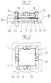
- a second exemplary embodiment of the contact arrangement according to the invention is shown. It essentially differs from the first exemplary embodiment in the formation of the compressible contact element 5, which is disposed in the space between the free end of the contact pin 3 facing the electrical component 1 and the terminal contact 6 facing the contact pin 3.
- This compressible contact element 5 comprises essentially a mat of silicone rubber having a thickness of about 0.3 to 1 mm. Disposed in the silicone rubber approximately at right angles to the plane defined by the mat are thin metal wires, preferably gold-plated wires. The individual little wires are spaced about 0.05 to 0.1 mm from one another. They are cut off approximately flush with the underside and the upper side of the mat.
- Such mats are commercially known and can, for example, be procured through the Japanese firm SHIN-ETSU. The firm indicates that these mats are suitable, for example, for electrically connecting electronic parts to conductor paths of a printed circuit board without a soldered joint.
- the plate-shaped support part 7 comprises essentially two superimposed plates 33, 34.
- the compressible mat 5 is disposed between the two plates.
- the fine wires which are disposed in the compressible mat 5 and which extend from the lower plate 33 to the upper plate 34 are marked with the reference numeral 10.
- the two superimposed plates are joined to one another in a suitable manner. They may be screwed together, held together by means of clamps, riveted, or held together in any other way.
- the mat 5 extends across all the bores 13.
- the contact pins 3 are pressed into the bores 13 of the lower plate 33, as previously described, and are contiguous with the underside of the lower plate 33 by means of the stop ring 30.
- each contact pin 3, not intended for connection with the printed circuit board 2 is substantially flush with the upper side of the lower plate 33. Preferably, it projects just a little from the bore 13.
- the end of the contact pin 3 which abuts the mat 5 is formed in such a way that contact-making takes place with as large a number of the thin wires 10 as possible. Simultaneously, it shall also be achieved that the end of the contact pin 3 can be pressed into the adjacent side of the mat without too great a force having to be mustered.
- the end of the contact pin 3 is either made as a multitoothed crown having relatively blunt teeth or that the end face of the contact pin is slightly dished, the dish rim forming a not too sharp-edged annulus.
- the substantially dome-shaped terminal contact 6 rests on the other side of the compressible or elastic mat 5.
- the electrical connection between the terminal contact 6 and the associated contact pin 3 takes place through the pressing-down of the electrical component 1 by the holding-down device 16, as has already been described previously.
- At least one, but preferably a plurality of the fine little wires 10, thereby reliably establish an electrical connection between the terminal contact 6 and the end of the contact pin 3.
- the bores 13 of the upper plate 34 serve merely to guide the terminal contacts 6 of the electrical component 1.
- the upper plate 34 is therefore made thinner than the lower plate 33.
- the holding-down device 16 is formed as a spring.
- the latter is designed in this case as an approximately rectangular ring, the corners of the ring being raised and each projecting in the mounted state under a respective screw head of a fastening screw 23. From each corner of the ring, about two legs extend obliquely downward at an angle of about 45°, the junctions of each two legs meeting from adjacent corners forming a pressure point designated as 28 by which the electrical component 1 is pressed down on the holding part 7.
- the spring comprises four spring pressure means 17, each pressure means pressing on a corner region of the electrical component 1.
- the spring force of the holding-down device 16 can be adjusted.
- the holding-down device 16 formed as a pressure spring in Fig. 9 might also take other forms or be disposed otherwise.
- the holding-down device shown might also be mounted in such a way that the pressure means 17 press on the electrical component 1 substantially about halfway along each longitudinal side.
- the fastening screws would then be disposed in the region of the corners of the component, i.e., the whole holding-down device would be turned by about 45° as compared with the exemplary embodiment shown.
- it might be provided, instead of the rectangular spring, to form the latter as a cross or in any other suitable shape.
- a cooling body might, as already mentioned previously, be disposed between the spring and the component in this exemplary embodiment as well.
- a further holding-down device 16 is shown.
- This one comprises, like the first and second exemplary embodiments, four holding-down elements, only one of which is shown and designated by the reference numeral 18 in Fig. 10.
- Depicted with the reference numeral 29 is a web plate which is clamped between the spacer 24 and the screw head of the fastening screw 23 and extends over the component 1.
- the web plate 29 has, for example, a tapped bore into which a setscrew 19 is screwed, the screw shank of this screw pressing the electrical component 1 down on the support part 7 more strongly or less strongly depending on the screwing-in depth.
- the setscrew is intended to be an adjustment means 19 for adjusting the holding-down force.
- the web plate 29 spans the entire electrical component 1 and is held on the other side of the component in the same way as shown in Fig. 10.
- a cooling body might be disposed, and the setscrew might press on the cooling body merely in the middle, for example, or there could be several setscrews along the web plate.
- the web plate 29 shown or the strip-shaped web plate described might also be formed rectangular and be held by means of four fastening screws similarly to the preceding examples. It might comprise several adjusting screws, or it might rest directly on the electrical component 1 and serve additionally as a cooling body.
Landscapes
- Engineering & Computer Science (AREA)
- Microelectronics & Electronic Packaging (AREA)
- Coupling Device And Connection With Printed Circuit (AREA)
- Connecting Device With Holders (AREA)
- Structures For Mounting Electric Components On Printed Circuit Boards (AREA)
- Multi-Conductor Connections (AREA)
Description
Claims (25)
- Contact arrangement for detachably attaching an electrical component (1) having a plurality of terminal contacts (6) to a printed circuit board (2), comprisinga support (7) disposable between said electrical component (1) and said printed circuit board (2) and comprising a plurality of bores (13) arranged in the same way as said terminal contacts (6),a number of electrically conductive contact pins (3) which are directly attachable to the printed circuit board (2) and in attached state extend away from the printed circuit board (2) at about right angles,each of the contact pins (3) being disposed in one of said bores (13) and being connectable to at least one conductor path of the printed circuit board (2) for establishing an electrical connection,the contact pins (3) are made in one piece,a space (9) extending away in each of said bores (13) from the free end of the contact pin (3) between each contact pin (3) and a therewith associated terminal contact (6) of an electrical component (1) when said electrical component is attached on said contact arrangement, andthe space (9) is bridged by an axially compressible, electrically conductive contact element (4, 5) for establishing an electrical connection between the contact pin (3) and the terminal contact (6) of the electrical component (1).
- Contact arrangement according to claim 1, wherein the electrical component (1) is an integrated circuit.
- Contact arrangement according to claim 1, wherein said terminal contacts (6) are disposed in a ball grid array (BGA).
- Contact arrangement according to claim 1, wherein said terminal contacts (6) are disposed in a column grid array (CGA).
- Contact arrangement according to claim 1, wherein said terminal contacts (6) are disposed in a land grid array (LGA).
- Contact arrangement according to claim 2, wherein said integrated circuit (1) is of the flip-chip type.
- Contact arrangement according to claim 1, wherein said electrical component (1) is a second printed circuit board, said contact arrangement being used for a board-to-board interconnection between both printed circuit boards.
- Contact arrangement according to claim 1 or 2, wherein the compressible, electrically conductive contact element is a coil spring (4).
- Contact arrangement according to claim 8, wherein the end of the contact pin pointing toward the terminal contact of the component has an extension (11) onto which the coil spring (4) can be pressed.
- Contact arrangement according to claim 1 or 2, wherein the compressible, electrically conductive contact element comprises an electrically insulating rubber-elastic mat (5) in which there are a plurality of thin wires spaced close to one another and running in axial direction to the contact pins (3).
- Contact arrangement according to claim 10, wherein the mat (5) extends at least over the entire area formed by the plurality of terminal contacts (6).
- Contact arrangement according to claim 10 or 11, wherein the end of the contact pin (3) facing the terminal contact of the component has a dish with a circular rim or a crown-shaped structure (12) with several teeth.
- Contact arrangement according to claim 1, characterized in that the contact pins (3) are formed as an SMD part (suiface mounted device) and are attached to the surface of the printed circuit board (2).
- Contact arrangement according to claim 1, wherein said support (7) is plate-shaped, and preferably made of an epoxy material or of a thermoplastic synthetic material, and wherein each contact pin (3) projects from said support (7) on the side facing the printed circuit board (2), and the other end of each contact pin being disposed set back from the support part surface facing the electrical component (1).
- Contact arrangement according to claim 14, wherein the plate-shaped support part (7) comprises two superimposed plates, the mat (5) being disposed between the two plates.
- Contact arrangement according to claim 14 or 15, wherein the contact pins (3) are pressed into the bores (13) of the support part (7).
- Contact arrangement according to claim 14, wherein the end region (14) of each bore (13) of the support part (7) facing the component (1) is formed as a guide means for the terminal contact (6) of the electrical component (1) associated with the respective bore (13).
- Contact arrangement according to claim 1, wherein for positioning the component (1) relative to the contact arrangement there are guide means substantially resting against lateral faces of the component (1).
- Contact arrangement according to claim 14, wherein there is a holding-down device (17) for pressing the terminal contacts (3) of the component (1) down on the compressible, electrically conductive contact element (4, 5), which device is fixed to the support part or to the printed circuit board and has a pressure means which presses at least one location upon the top surface of the component (1) remote from the printed circuit board (2).
- Contact arrangement according to claim 19, wherein the holding-down device (17) comprises a spring (17) pressing on the component (1).
- Contact arrangement according to claim 19, wherein the holding-down device (17) comprises at least one non-spring (18) holding-down element which is connected to the support part on one side and presses upon the side of the component (1) remote from the printed circuit board (2) on the other side.
- Contact arrangement according to claim 14, wherein the holding-down device comprises an adjustment means (23) by which the holding-down pressure is adjustable.
- Contact arrangement according to claim 14, wherein the distance from one edge of the support part to the nearest contact pin (3) is at most 0.21 inch (5.2 mm).
- Contact arrangement according to claim 14, wherein the contact pins (3) inserted in the support part (7) and the support part (7) together form a connector block, the maximum overall height of the connector block disposed on the printed circuit board (2) amounting to at most 0.16 inch (4.1 mm).
- Contact arrangement for detachably attaching an electrical component (1) having a plurality of terminal contacts (6) to a printed circuit board (2) comprising :a plate-shaped support part (7),continuous bores (13) in the support part (7),a number of electrically conductive contact pins (3) which are directly attachable to the printed circuit board (2) and in attached state extend away from the printed circuit board (2),each contact pin (3) extends through one of the continuous bores (13) in the support part (7),a free end of each contact pin (3) being disposed set back from the support part (7) surface facing the eiectrical component (1), forming a space (9) extending between said free end of the contact pin (3) and a therewith associated terminal contact (6) of the electrical component when attached on the contact arrangement, anda compressible, electrically conductive contact element (4, 5) bridging the said space (9) for establishing an electrical connection between the contact pin (3) and the terminal contact (6) of the electrical component (1).
Priority Applications (1)
| Application Number | Priority Date | Filing Date | Title |
|---|---|---|---|
| EP96919752A EP0829188B1 (en) | 1995-05-26 | 1996-05-10 | Contact arrangement for detachably attaching an electric component, especially an integrated circuit to a printed circuit board |
Applications Claiming Priority (6)
| Application Number | Priority Date | Filing Date | Title |
|---|---|---|---|
| EP95810352 | 1995-05-26 | ||
| EP95810352 | 1995-05-26 | ||
| US53915895A | 1995-10-04 | 1995-10-04 | |
| US539158 | 1995-10-04 | ||
| PCT/EP1996/001987 WO1996038030A1 (en) | 1995-05-26 | 1996-05-10 | Contact arrangement for detachably attaching an electric component, especially an integrated circuit to a printed circuit board |
| EP96919752A EP0829188B1 (en) | 1995-05-26 | 1996-05-10 | Contact arrangement for detachably attaching an electric component, especially an integrated circuit to a printed circuit board |
Publications (2)
| Publication Number | Publication Date |
|---|---|
| EP0829188A1 EP0829188A1 (en) | 1998-03-18 |
| EP0829188B1 true EP0829188B1 (en) | 1999-08-04 |
Family
ID=26140677
Family Applications (1)
| Application Number | Title | Priority Date | Filing Date |
|---|---|---|---|
| EP96919752A Expired - Lifetime EP0829188B1 (en) | 1995-05-26 | 1996-05-10 | Contact arrangement for detachably attaching an electric component, especially an integrated circuit to a printed circuit board |
Country Status (8)
| Country | Link |
|---|---|
| EP (1) | EP0829188B1 (en) |
| JP (1) | JP3266620B2 (en) |
| KR (1) | KR100293624B1 (en) |
| CN (1) | CN1098620C (en) |
| AU (1) | AU5817396A (en) |
| CA (1) | CA2222049A1 (en) |
| DE (1) | DE69603600T2 (en) |
| WO (1) | WO1996038030A1 (en) |
Cited By (1)
| Publication number | Priority date | Publication date | Assignee | Title |
|---|---|---|---|---|
| US6992496B2 (en) | 2002-03-05 | 2006-01-31 | Rika Electronics International, Inc. | Apparatus for interfacing electronic packages and test equipment |
Families Citing this family (6)
| Publication number | Priority date | Publication date | Assignee | Title |
|---|---|---|---|---|
| US5791914A (en) * | 1995-11-21 | 1998-08-11 | Loranger International Corporation | Electrical socket with floating guide plate |
| US5877554A (en) * | 1997-11-03 | 1999-03-02 | Advanced Interconnections Corp. | Converter socket terminal |
| EP0919886A1 (en) * | 1997-11-27 | 1999-06-02 | Andreas Haller GmbH & Co. KG Fabrik für Feinmechanik | Electric watch |
| US6256202B1 (en) | 2000-02-18 | 2001-07-03 | Advanced Interconnections Corporation | Integrated circuit intercoupling component with heat sink |
| EP4293994A4 (en) * | 2021-05-10 | 2024-10-09 | Samsung Electronics Co., Ltd. | PRINTED CIRCUIT BOARD CONNECTOR AND ELECTRONIC DEVICE THEREOF |
| DE102024129307A1 (en) * | 2024-10-10 | 2026-04-16 | ProMik Programmiersysteme für die Mikroelektronik GmbH | Device for programming a customer circuit board |
Family Cites Families (8)
| Publication number | Priority date | Publication date | Assignee | Title |
|---|---|---|---|---|
| DE2715056C3 (en) * | 1977-04-04 | 1979-10-11 | Siemens Ag, 1000 Berlin Und 8000 Muenchen | Holder for a substrate in a microwave assembly |
| US4498721A (en) * | 1982-09-16 | 1985-02-12 | Amp Incorporated | Electrical connector for an electronic package |
| US4642889A (en) * | 1985-04-29 | 1987-02-17 | Amp Incorporated | Compliant interconnection and method therefor |
| US4916523A (en) * | 1988-09-19 | 1990-04-10 | Advanced Micro Devices, Inc. | Electrical connections via unidirectional conductive elastomer for pin carrier outside lead bond |
| US4922376A (en) * | 1989-04-10 | 1990-05-01 | Unistructure, Inc. | Spring grid array interconnection for active microelectronic elements |
| US5321583A (en) * | 1992-12-02 | 1994-06-14 | Intel Corporation | Electrically conductive interposer and array package concept for interconnecting to a circuit board |
| US5376010A (en) * | 1994-02-08 | 1994-12-27 | Minnesota Mining And Manufacturing Company | Burn-in socket |
| FI962692A7 (en) * | 1996-06-28 | 1997-12-29 | Nokia Corp | Touchscreen and terminal |
-
1996
- 1996-05-10 EP EP96919752A patent/EP0829188B1/en not_active Expired - Lifetime
- 1996-05-10 JP JP53531496A patent/JP3266620B2/en not_active Expired - Lifetime
- 1996-05-10 DE DE69603600T patent/DE69603600T2/en not_active Expired - Lifetime
- 1996-05-10 WO PCT/EP1996/001987 patent/WO1996038030A1/en not_active Ceased
- 1996-05-10 AU AU58173/96A patent/AU5817396A/en not_active Abandoned
- 1996-05-10 CA CA002222049A patent/CA2222049A1/en not_active Abandoned
- 1996-05-10 CN CN96195554A patent/CN1098620C/en not_active Expired - Lifetime
- 1996-05-10 KR KR1019970708446A patent/KR100293624B1/en not_active Expired - Lifetime
Cited By (2)
| Publication number | Priority date | Publication date | Assignee | Title |
|---|---|---|---|---|
| US6992496B2 (en) | 2002-03-05 | 2006-01-31 | Rika Electronics International, Inc. | Apparatus for interfacing electronic packages and test equipment |
| US7362114B2 (en) | 2002-03-05 | 2008-04-22 | Rika Electronics International, Inc. | Apparatus for interfacing electronic packages and test equipment |
Also Published As
| Publication number | Publication date |
|---|---|
| WO1996038030A1 (en) | 1996-11-28 |
| DE69603600D1 (en) | 1999-09-09 |
| AU5817396A (en) | 1996-12-11 |
| CN1098620C (en) | 2003-01-08 |
| KR19990021971A (en) | 1999-03-25 |
| KR100293624B1 (en) | 2001-09-17 |
| CA2222049A1 (en) | 1996-11-28 |
| CN1191062A (en) | 1998-08-19 |
| DE69603600T2 (en) | 2000-02-10 |
| EP0829188A1 (en) | 1998-03-18 |
| JP3266620B2 (en) | 2002-03-18 |
| JPH11505953A (en) | 1999-05-25 |
Similar Documents
| Publication | Publication Date | Title |
|---|---|---|
| US6249440B1 (en) | Contact arrangement for detachably attaching an electric component, especially an integrated circuit to a printed circuit board | |
| US7682165B2 (en) | Electrical contact with retaining device for clipping solder ball | |
| US8821191B2 (en) | Electrical connector assembly | |
| EP1326308B1 (en) | Spring element, press-clamped connector, and holder with probe for electro-acoustic component | |
| US7553202B2 (en) | Electrical terminal | |
| US4252390A (en) | Low insertion force electrical retainer | |
| US20030017726A1 (en) | Elastomeric connector interconnecting flexible circuits and circuit board and method of manufacturing the same | |
| US6109927A (en) | Connector for adjacent circuit-bearing substrates | |
| US6731516B1 (en) | Land grid array connector having movable engagement of electrical contacts thereinto | |
| US5288238A (en) | IC chip to PC board connector system | |
| WO2005018296A1 (en) | Land grid array connector | |
| US5487674A (en) | Surface mountable leaded package | |
| WO1996038030A1 (en) | Contact arrangement for detachably attaching an electric component, especially an integrated circuit to a printed circuit board | |
| US6899565B2 (en) | Electrical connector having a holddown for ground connection | |
| US7128580B2 (en) | Socket connector with supporting housing protrusions | |
| US6471535B1 (en) | Electrical socket | |
| US20020168883A1 (en) | Connectors for circuit boards configured | |
| US6095857A (en) | Electrical component for surface-mounting on a circuit board | |
| KR102104282B1 (en) | Integral printed circuit board assembly with terminal | |
| JPH08512168A (en) | High-density electronic device connector | |
| US20030220007A1 (en) | Electrical connector with distortion-resistant cover | |
| JP2004257831A (en) | Contacts and electrical connection devices | |
| EP0903810A2 (en) | Connector for adjacent circuit-bearing substrates | |
| JP4142222B2 (en) | Semiconductor device holder | |
| JP2667628B2 (en) | Alignment device for contact points in IC socket |
Legal Events
| Date | Code | Title | Description |
|---|---|---|---|
| PUAI | Public reference made under article 153(3) epc to a published international application that has entered the european phase |
Free format text: ORIGINAL CODE: 0009012 |
|
| 17P | Request for examination filed |
Effective date: 19971119 |
|
| AK | Designated contracting states |
Kind code of ref document: A1 Designated state(s): CH DE FR GB IE IT LI |
|
| 17Q | First examination report despatched |
Effective date: 19980325 |
|
| GRAG | Despatch of communication of intention to grant |
Free format text: ORIGINAL CODE: EPIDOS AGRA |
|
| GRAG | Despatch of communication of intention to grant |
Free format text: ORIGINAL CODE: EPIDOS AGRA |
|
| GRAH | Despatch of communication of intention to grant a patent |
Free format text: ORIGINAL CODE: EPIDOS IGRA |
|
| GRAH | Despatch of communication of intention to grant a patent |
Free format text: ORIGINAL CODE: EPIDOS IGRA |
|
| GRAA | (expected) grant |
Free format text: ORIGINAL CODE: 0009210 |
|
| AK | Designated contracting states |
Kind code of ref document: B1 Designated state(s): CH DE FR GB IE IT LI |
|
| REG | Reference to a national code |
Ref country code: CH Ref legal event code: EP |
|
| REF | Corresponds to: |
Ref document number: 69603600 Country of ref document: DE Date of ref document: 19990909 |
|
| ITF | It: translation for a ep patent filed | ||
| REG | Reference to a national code |
Ref country code: IE Ref legal event code: FG4D |
|
| REG | Reference to a national code |
Ref country code: CH Ref legal event code: NV Representative=s name: BOVARD AG PATENTANWAELTE |
|
| ET | Fr: translation filed | ||
| REG | Reference to a national code |
Ref country code: CH Ref legal event code: NV Representative=s name: PATENTS & TECHNOLOGY SURVEYS, FORNEROD & SAAM |
|
| PLBE | No opposition filed within time limit |
Free format text: ORIGINAL CODE: 0009261 |
|
| STAA | Information on the status of an ep patent application or granted ep patent |
Free format text: STATUS: NO OPPOSITION FILED WITHIN TIME LIMIT |
|
| 26N | No opposition filed | ||
| REG | Reference to a national code |
Ref country code: GB Ref legal event code: IF02 |
|
| REG | Reference to a national code |
Ref country code: CH Ref legal event code: PCAR Representative=s name: PATENTS & TECHNOLOGY SURVEYS SA, CH |
|
| PGFP | Annual fee paid to national office [announced via postgrant information from national office to epo] |
Ref country code: IE Payment date: 20070524 Year of fee payment: 12 |
|
| PGFP | Annual fee paid to national office [announced via postgrant information from national office to epo] |
Ref country code: IT Payment date: 20070514 Year of fee payment: 12 |
|
| REG | Reference to a national code |
Ref country code: IE Ref legal event code: MM4A |
|
| PG25 | Lapsed in a contracting state [announced via postgrant information from national office to epo] |
Ref country code: IE Free format text: LAPSE BECAUSE OF NON-PAYMENT OF DUE FEES Effective date: 20080512 |
|
| PG25 | Lapsed in a contracting state [announced via postgrant information from national office to epo] |
Ref country code: IT Free format text: LAPSE BECAUSE OF NON-PAYMENT OF DUE FEES Effective date: 20080510 |
|
| REG | Reference to a national code |
Ref country code: CH Ref legal event code: PFA Owner name: E-TEC AG Free format text: E-TEC AG#FRIEDHOFSTRASSE 1#CH-2543 LENGNAU (CH) -TRANSFER TO- E-TEC AG#FRIEDHOFSTRASSE 1#CH-2543 LENGNAU (CH) |
|
| REG | Reference to a national code |
Ref country code: FR Ref legal event code: PLFP Year of fee payment: 20 |
|
| PGFP | Annual fee paid to national office [announced via postgrant information from national office to epo] |
Ref country code: GB Payment date: 20150521 Year of fee payment: 20 Ref country code: DE Payment date: 20150521 Year of fee payment: 20 Ref country code: CH Payment date: 20150521 Year of fee payment: 20 |
|
| PGFP | Annual fee paid to national office [announced via postgrant information from national office to epo] |
Ref country code: FR Payment date: 20150521 Year of fee payment: 20 |
|
| REG | Reference to a national code |
Ref country code: DE Ref legal event code: R071 Ref document number: 69603600 Country of ref document: DE |
|
| REG | Reference to a national code |
Ref country code: CH Ref legal event code: PL |
|
| REG | Reference to a national code |
Ref country code: GB Ref legal event code: PE20 Expiry date: 20160509 |
|
| PG25 | Lapsed in a contracting state [announced via postgrant information from national office to epo] |
Ref country code: GB Free format text: LAPSE BECAUSE OF EXPIRATION OF PROTECTION Effective date: 20160509 |