EP0821149B1 - Device for controlling inductive loads, in particular of injectors of an internal combustion engine injection system - Google Patents
Device for controlling inductive loads, in particular of injectors of an internal combustion engine injection system Download PDFInfo
- Publication number
- EP0821149B1 EP0821149B1 EP97112560A EP97112560A EP0821149B1 EP 0821149 B1 EP0821149 B1 EP 0821149B1 EP 97112560 A EP97112560 A EP 97112560A EP 97112560 A EP97112560 A EP 97112560A EP 0821149 B1 EP0821149 B1 EP 0821149B1
- Authority
- EP
- European Patent Office
- Prior art keywords
- transistor
- terminal
- diode
- timing
- terminal connected
- Prior art date
- Legal status (The legal status is an assumption and is not a legal conclusion. Google has not performed a legal analysis and makes no representation as to the accuracy of the status listed.)
- Expired - Lifetime
Links
Images


Classifications
-
- F—MECHANICAL ENGINEERING; LIGHTING; HEATING; WEAPONS; BLASTING
- F02—COMBUSTION ENGINES; HOT-GAS OR COMBUSTION-PRODUCT ENGINE PLANTS
- F02D—CONTROLLING COMBUSTION ENGINES
- F02D41/00—Electrical control of supply of combustible mixture or its constituents
- F02D41/30—Controlling fuel injection
- F02D41/3005—Details not otherwise provided for
-
- F—MECHANICAL ENGINEERING; LIGHTING; HEATING; WEAPONS; BLASTING
- F02—COMBUSTION ENGINES; HOT-GAS OR COMBUSTION-PRODUCT ENGINE PLANTS
- F02D—CONTROLLING COMBUSTION ENGINES
- F02D41/00—Electrical control of supply of combustible mixture or its constituents
- F02D41/20—Output circuits, e.g. for controlling currents in command coils
- F02D2041/2003—Output circuits, e.g. for controlling currents in command coils using means for creating a boost voltage, i.e. generation or use of a voltage higher than the battery voltage, e.g. to speed up injector opening
- F02D2041/2006—Output circuits, e.g. for controlling currents in command coils using means for creating a boost voltage, i.e. generation or use of a voltage higher than the battery voltage, e.g. to speed up injector opening by using a boost capacitor
-
- F—MECHANICAL ENGINEERING; LIGHTING; HEATING; WEAPONS; BLASTING
- F02—COMBUSTION ENGINES; HOT-GAS OR COMBUSTION-PRODUCT ENGINE PLANTS
- F02D—CONTROLLING COMBUSTION ENGINES
- F02D41/00—Electrical control of supply of combustible mixture or its constituents
- F02D41/20—Output circuits, e.g. for controlling currents in command coils
- F02D2041/2017—Output circuits, e.g. for controlling currents in command coils using means for creating a boost current or using reference switching
-
- F—MECHANICAL ENGINEERING; LIGHTING; HEATING; WEAPONS; BLASTING
- F02—COMBUSTION ENGINES; HOT-GAS OR COMBUSTION-PRODUCT ENGINE PLANTS
- F02D—CONTROLLING COMBUSTION ENGINES
- F02D41/00—Electrical control of supply of combustible mixture or its constituents
- F02D41/20—Output circuits, e.g. for controlling currents in command coils
- F02D2041/202—Output circuits, e.g. for controlling currents in command coils characterised by the control of the circuit
- F02D2041/2044—Output circuits, e.g. for controlling currents in command coils characterised by the control of the circuit using pre-magnetisation or post-magnetisation of the coils
-
- F—MECHANICAL ENGINEERING; LIGHTING; HEATING; WEAPONS; BLASTING
- F02—COMBUSTION ENGINES; HOT-GAS OR COMBUSTION-PRODUCT ENGINE PLANTS
- F02D—CONTROLLING COMBUSTION ENGINES
- F02D41/00—Electrical control of supply of combustible mixture or its constituents
- F02D41/20—Output circuits, e.g. for controlling currents in command coils
- F02D2041/2068—Output circuits, e.g. for controlling currents in command coils characterised by the circuit design or special circuit elements
- F02D2041/2072—Bridge circuits, i.e. the load being placed in the diagonal of a bridge to be controlled in both directions
-
- F—MECHANICAL ENGINEERING; LIGHTING; HEATING; WEAPONS; BLASTING
- F02—COMBUSTION ENGINES; HOT-GAS OR COMBUSTION-PRODUCT ENGINE PLANTS
- F02D—CONTROLLING COMBUSTION ENGINES
- F02D41/00—Electrical control of supply of combustible mixture or its constituents
- F02D41/20—Output circuits, e.g. for controlling currents in command coils
- F02D2041/2068—Output circuits, e.g. for controlling currents in command coils characterised by the circuit design or special circuit elements
- F02D2041/2075—Type of transistors or particular use thereof
Definitions
- the present invention relates to a device for controlling inductive loads, in particular of injectors of an internal combustion engine injection system.
- each injector must be supplied with current, the curve of which comprises a rapidly increasing portion, a more slowly increasing portion, a portion decreasing to a hold value, a portion oscillating about the hold value, and a portion decreasing to zero.
- control devices are currently employed whereby the inductive loads of the injectors are connected on one side to a low-voltage supply source, and on the other side to a ground line via a controlled electronic switch.
- a major drawback of control devices of this sort is that, in the event of ground shorting of one of the terminals of any one of the inductive loads - e.g. due to impaired insulation of of an injector conductor, and contact between the conductor and the vehicle body - the injector and/or control device is irreparably damaged and the engine is turned off - an extremely dangerous situation when the vehicle is moving.
- Such a device using three switching transistors and an energy storing capacitor is known from FR-A-2538942.
- control devices have been proposed whereby the inductive loads of the injectors are grounded on one side and connected on the other side to an internal node of the control device itself, so that, as opposed to damaging the control device and turning off the engine, ground shorting of one of the terminals of the inductive loads simply results in that particular injector being put out of use, so that the vehicle continues running minus one injector.
- control devices in addition to involving complex, high-cost circuitry, normally fail to provide for simultaneously injecting different cylinders, as required for example by engine injection systems involving multiple injection of each cylinder.
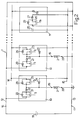
- Number 1 in Figure 1 indicates a device for controlling the control electromagnets of injectors 3 of an injection system 4 of an internal combustion engine 5, in particular a supercharged diesel engine.
- the control electromagnets are represented by the electric equivalents comprising inductors 2.
- Control device 1 comprises a timing circuit 6 receiving information signals S measured on engine 5, and generating timing signals T for controlling injectors 3; and a modular circuit 7 receiving timing signals T and for driving injectors 3 accordingly.
- Modular circuit 7 comprises a number of modular circuits 10, one for each inductor 2, activated selectively and receiving timing signals T as described in detail later on; and a common circuit 11 connected to modular circuits 10 and cooperating with the activated modular circuit 10 to supply respective inductor 2 as also described in detail later on.
- modular circuit 7 comprises a supply line 12; a ground line 13; and a first and second connecting line 14, 15 between modular circuits 10 and common circuit 11.
- Modular circuit 7 also comprises a first and second input terminal 16, 17 respectively connectable to a positive pole and a negative pole of a supply source, e.g. a battery 18; and a number of pairs of output terminals, one for each injector 3.
- Each pair of output terminals comprises a first and second output terminal 19, 20 between which a respective inductor 2 is connected in use. More specifically, the first input terminal 16 of modular circuit 7 is connected to supply line 12, and the second input terminal 17 and the second output terminals 20 are connected to ground line 13.
- Each modular circuit 10 comprises a MOSFET charging transistor 21 having a control terminal connected to timing circuit 6 and receiving from timing circuit 6 a first timing signal T 1 , a drain terminal connected to supply line 12, and a source terminal connected to the anode of a charging diode 22, the cathode of which is connected to a respective first output terminal 19 of modular circuit 7.
- Modular circuit 10 also comprises a MOSFET discharging transistor 23 having a control terminal connected to timing circuit 6 and receiving from timing circuit 6 a second timing signal T 2 , a drain terminal connected to first connecting line 14, and a source terminal connected to respective first output terminal 19 of modular circuit 7.
- Modular circuit 10 also comprises a clamping diode 24 with the anode connected to second connecting line 15, and the cathode connected to respective first output terminal 19 of modular circuit 7.
- Common circuit 11 comprises a capacitor 25 having a first and second terminal connected respectively to first connecting line 14 and second connecting line 15.
- Common circuit 11 also comprises a MOSFET recirculating transistor 26 having a control terminal connected to timing circuit 6 and receiving from timing circuit 6 a third timing signal T 3 , a drain terminal connected to ground line 13, and a source terminal connected to the anode of a recirculating diode 27, the cathode of which is connected to second connecting line 15.
- a MOSFET recirculating transistor 26 having a control terminal connected to timing circuit 6 and receiving from timing circuit 6 a third timing signal T 3 , a drain terminal connected to ground line 13, and a source terminal connected to the anode of a recirculating diode 27, the cathode of which is connected to second connecting line 15.
- Common circuit 11 also comprises a discharging diode 28 with the anode connected to ground line 13, and the cathode connected to first connecting line 14.
- each transistor 21, 23, 26 of modular circuits 10 and common circuit 11 are connected respectively to the cathode and anode of a respective protection diode 29 operating in known manner and therefore not described in detail.
- Timing circuit 6 selectively activates each modular circuit 10 by supplying the control terminals of transistors 21, 23, 26 with timing signals T 1 , T 2 , T 3 , which are only supplied to the modular circuit to be activated, so that the other modular circuits 10 remain off. Furthermore, timing signals T 1 , T 2 , T 3 , control MOSFET transistors 21, 23, 26 to saturate them or to switch them off, so that each transistor acts as a closed or open switch.
- control device 1 Operation of control device 1 will now be described with reference to one injector 3 and one modular circuit 10 - the other modular circuits - operating in the same way - which cooperates with common circuit 11 to supply respective inductor 2, and with specific reference to Figures 3 to 7 showing time graphs of timing signals T 1 , T 2 , T 3 of transistors 21, 23, 26, the voltage V C of capacitor 25, and the current flow I L in inductor 2.
- timing circuit 6 opens all of transistors 21, 23, 26, so that both modular circuit 10 and common circuit 11 are off.
- Timing circuit 6 then closes and opens, several times in succession, the charging transistor 21 of the modular circuit 10 activated at the time, by supplying the control terminal of charging transistor 21 with a train of so-called recharging pulses, as shown in Figure 3 (RECHARGING PHASE). More specifically, when charging transistor 21 is closed (instant t 0 in Figure 3), a closed loop is formed comprising battery 18, charging transistor 21, charging diode 22 and inductor 2; and inductor 2, being supplied by battery 18 with a constant voltage, is supplied with an increasing current, which increases the energy stored in inductor 2.
- capacitor 25 and inductor 2 are connected to each other in series via discharging diode 28 and clamping diode 24 to form a resonant circuit, so that current flows in the loop defined by inductor 2, discharging diode 28, capacitor 25 and clamping diode 24, thus charging capacitor 25 and increasing the voltage at the terminals of capacitor 25, so that the energy stored in inductor 2 is transferred, minus any losses, to capacitor 25.
- Timing circuit 6 then closes recirculating transistor 23 and discharging transistor 26 sequentially (instant t 2 in Figures 4 and 5) to form a further closed loop comprising capacitor 25, inductor 2, transistors 23, 26 and recirculating diode 27, and so form a further resonant circuit, so that a current flow is generated to discharge capacitor 25, reduce the voltage at the terminals of capacitor 25, and transfer all the energy stored in capacitor 25 to inductor 2, as shown in Figure 6 (RESONANT DISCHARGE PHASE).
- charging diode 22 Upon the voltage at the terminals of capacitor 25 reaching a value V 2 equal to the voltage of battery 18 minus the threshold voltage of charging diode 22, charging diode 22 begins conducting and again connects inductor 2 in series with battery 18, which supplies inductor 2 with a constant voltage, so that the inductor is supplied with increasing current to keep injector 3 open (BYPASS PHASE). The current flow in inductor 2 therefore continues increasing, as shown in Figure 7, but at a slower rate than before.
- timing circuit 6 opens discharging transistor 23 (instant t 3 in Figure 4), recirculating transistor 26 (instant t 4 in Figure 5) and charging transistor 21 (instant t 5 in Figure 3) to form a closed loop comprising capacitor 25, inductor 2 (which combine to form a resonant circuit), clamping diode 24 and discharging diode 28, and to generate a current flow to charge capacitor 25 and discharge inductor 2 (DELAY PHASE).
- Discharging inductor 2 permits recharging of capacitor 25, thus reducing the number of recharging pulses required in the next drive cycle, and hence recharging time, and also reducing the time interval between one injection and the next.
- timing circuit 6 closes and opens charging transistor 21 several times in succession by supplying a train of pulses to the control terminal, and the current flow in inductor 2 assumes a saw-tooth pattern oscillating about a predetermined mean value sufficient to keep injector 3 open.
- timing circuit 6 closes charging transistor 21 (instant t 7 ), so that inductor 2 is once more connected in series with battery 18 via charging transistor 21 and charging diode 22; the current flow in inductor 2 therefore increases to charge inductor 2 (CHOPPER ON PHASE) until timing circuit 6 opens charging transistor 21 (instant t 8 in Figure 3) to disconnect inductor 2 from battery 18, so that current is supplied to the loop defined by inductor 2, recirculating transistor 26, recirculating diode 27 and clamping diode 24; which current partially discharges inductor 2 (CHOPPER OFF PHASE) until timing circuit 6 again closes charging transistor 21, and the CHOPPER ON PHASE is repeated.
- timing circuit 6 sequentially opens recirculating transistor 26 and charging transistor 21 (instants t 9 and t 10 in Figures 5 and 6), so that capacitor 25 and inductor 2 are once more connected in series via clamping diode 24 and discharging diode 28 to form a resonant circuit, and the discharge current of inductor 2 charges and increases the voltage of capacitor 25 (RESONANT RECHARGING PHASE). This phase continues until inductor 2 is completely discharged, thus terminating the drive cycle of injector 3; at which point, timing circuit 6 may commence a further drive cycle of another injector 3 as described above.
- control device 1 The advantages of control device 1 are as follows. Firstly, by virtue of each inductor 2 being connected to control device 1 as described above, ground shorting of one of the terminals of inductor 2 in no way damages injector 3 or control device 1, but simply results in exclusion of injector 3, with no impairment in the operation of the other injectors 3, and without the engine suddenly being turned off.
- control device 1 provides for simultaneously driving a number of injectors 3, e.g. as in the case of multiple injections in some of the cylinders of engine 5.
- a number of injectors e.g. as in the case of multiple injections in some of the cylinders of engine 5.
- capacitor 25 is again charged and capable of enabling the RESONANT DISCHARGING phase to drive another injector 3.
Landscapes
- Engineering & Computer Science (AREA)
- Chemical & Material Sciences (AREA)
- Combustion & Propulsion (AREA)
- Mechanical Engineering (AREA)
- General Engineering & Computer Science (AREA)
- Electrical Control Of Air Or Fuel Supplied To Internal-Combustion Engine (AREA)
- Fuel-Injection Apparatus (AREA)
Description
Claims (14)
- A device (1) for controlling inductive loads (2), in particular of injectors (3) of an injection system (4) of an internal combustion engine (5), comprising:said drive means (7) also comprising a common circuit (11) comprising energy storing means (25); said common circuit being connected to the modular circuits (10) and cooperating with the activated modular circuit (10) to supply a respective inductive load (2);timing means (6) generating timing signals (T) for controlling said injectors (3);drive means (7) for driving said inductive loads (2) and comprising a number of modular circuits (10), one for each inductive load (2); said modular circuits being activated selectively and receiving said timing signals (T);
said drive means (7) also comprising a first and a second input terminal (16, 17) respectively connected, in use, to a positive pole and a negative pole of a supply source (18); and a number of pairs of output terminals, one for each injector (3); each pair of output terminals comprising a first and a second output terminal (19, 20) between which a respective inductive load (2) is connected in use; wherein
each of said modular circuits (10) comprises, in combination:and in that said common circuit (11) comprises:first controlled switching means (21, 22) connected between said first input terminal (16) and the respective first output terminal (19) of said drive means (7); andsecond controlled switching means (23, 24) connected between said respective first output terminal (19) and said energy storing means (25);third controlled switching means (26, 27, 28) connected between said energy storing means (25) and the respective second output terminal (20) of said drive means (7); said third controlled switching means (26, 27, 28) cooperating with said second controlled switching means (23, 24) to permit selective transfer of energy between said energy storing means (25) and said respective inductive load (2). - A device as claimed in Claim 1, characterized in that said drive means (7) also comprise a first and a second reference potential line (12, 13), and a first and a second connecting line (14, 15) between said modular circuits (10) and said common circuit (11); said first input terminal (16) being connected to said first reference potential line (12); and said second input and output terminals being connected to said second reference potential line (13).
- A device as claimed in Claim 2, characterized in that said first controlled switching means (21, 22) comprise first transistor means (21) and a first unipolar switch (22) connected to each other in series.
- A device as claimed in Claim 3, characterized in that said first transistor means comprise a charging transistor (21), and said first unipolar switch comprises a charging diode (22).
- A device as claimed in Claim 4, characterized in that said charging transistor (21) has a control terminal connected to said timing means (6) and receiving from said timing means (6) a first (T1) of said timing signals, a first terminal connected to said first reference potential line (12), and a second terminal connected to an anode terminal of said charging diode (22); said charging diode having a cathode terminal connected to said respective first output terminal (19) of said drive means (7).
- A device as claimed in any one of the foregoing Claims from 2 to 5, characterized in that said second controlled switching means (23, 24) comprise second transistor means (23) and a second unipolar switch (24), both having respective first terminals connected together to said respective first output terminal (19) of said drive means (7), and respective second terminals connected to said energy storing means (25).
- A device as claimed in Claim 6, characterized in that said second transistor means comprise a discharging transistor (23), and said second unipolar switch comprises a clamping diode (24).
- A device as claimed in Claim 7, characterized in that said discharging transistor (23) has a control terminal connected to said timing means (6) and receiving from said timing means (6) a second (T2) of said timing signals, a first terminal connected to said first connecting line (14), and a second terminal connected to said respective first output terminal (19) of said drive means (7); said clamping diode (24) having an anode terminal connected to said second connecting line (15), and a cathode terminal connected to said respective first output terminal (19) of said drive means (7).
- A device as claimed in any one of the foregoing Claims from 2 to 8, characterized in that said third controlled switching means (26, 27, 28) comprise third transistor means (26) and a third unipolar switch (27) connected to each other in series; said third controlled switching means (26, 27, 28) also comprising a fourth unipolar switch (28) connected between said first connecting line (14) and said second reference potential line (13).
- A device as claimed in Claim 9, characterized in that said third transistor means comprise a recirculating transistor (26); said third unipolar switch comprises a recirculating diode (27); and said fourth unipolar switch comprises a discharging diode (28).
- A device as claimed in Claim 10, characterized in that said recirculating transistor (26) has a control terminal connected to said timing means (6) and receiving from said timing means (6) a third (T3) of said timing signals, a first terminal connected to said second reference potential line (13), and a second terminal connected to an anode terminal of said recirculating diode (27); said recirculating diode having a cathode terminal connected to said second connecting line (15); and said discharging diode (28) having an anode terminal connected to said second reference potential line (13), and a cathode terminal connected to said first connecting line (14).
- A device as claimed in Claims 6, 8, 10, characterized in that said charging transistor (21), said discharging transistor (23) and said recirculating transistor (26) are MOSFET transistors.
- A device as claimed in Claims 7, 9, 11, characterized by comprising a protection diode (29) connected between said first and second terminal of each of said charging, discharging and recirculating transistors (21, 23, 26).
- A device as claimed in any one of the foregoing Claims from 2 to 13, characterized in that said energy storing means comprise a capacitive element (25) connected between said first and second connecting line (14, 15).
Applications Claiming Priority (2)
| Application Number | Priority Date | Filing Date | Title |
|---|---|---|---|
| ITTO960637 | 1996-07-23 | ||
| IT96TO000637A IT1284693B1 (en) | 1996-07-23 | 1996-07-23 | DEVICE FOR CONTROL OF INDUCTIVE LOADS, ESPECIALLY OF INJECTORS IN AN INJECTION SYSTEM FOR A COMBUSTION ENGINE |
Publications (2)
| Publication Number | Publication Date |
|---|---|
| EP0821149A1 EP0821149A1 (en) | 1998-01-28 |
| EP0821149B1 true EP0821149B1 (en) | 2001-11-21 |
Family
ID=11414812
Family Applications (1)
| Application Number | Title | Priority Date | Filing Date |
|---|---|---|---|
| EP97112560A Expired - Lifetime EP0821149B1 (en) | 1996-07-23 | 1997-07-22 | Device for controlling inductive loads, in particular of injectors of an internal combustion engine injection system |
Country Status (5)
| Country | Link |
|---|---|
| US (1) | US5877931A (en) |
| EP (1) | EP0821149B1 (en) |
| DE (1) | DE69708408T2 (en) |
| ES (1) | ES2168550T3 (en) |
| IT (1) | IT1284693B1 (en) |
Families Citing this family (6)
| Publication number | Priority date | Publication date | Assignee | Title |
|---|---|---|---|---|
| DE19719602A1 (en) * | 1997-05-09 | 1998-11-12 | Fahrzeugklimaregelung Gmbh | Electronic control circuit |
| US6175484B1 (en) * | 1999-03-01 | 2001-01-16 | Caterpillar Inc. | Energy recovery circuit configuration for solenoid injector driver circuits |
| IT1320679B1 (en) * | 2000-09-29 | 2003-12-10 | Fiat Ricerche | CONTROL DEVICE OF A COMMAND ELECTROMAGNET OF A DOSING VALVE OF A FUEL INJECTOR FOR A ENGINE |
| KR100367930B1 (en) * | 2001-12-26 | 2003-01-15 | Lucky Day Information & Comm C | Current inducing switch |
| US7057870B2 (en) * | 2003-07-17 | 2006-06-06 | Cummins, Inc. | Inductive load driver circuit and system |
| US9611797B2 (en) * | 2012-10-30 | 2017-04-04 | National Instruments Corporation | Direct injection flexible multiplexing scheme |
Family Cites Families (13)
| Publication number | Priority date | Publication date | Assignee | Title |
|---|---|---|---|---|
| FR2370216A1 (en) * | 1976-11-05 | 1978-06-02 | Renault | CONTROL DEVICE BY CURRENT PROGRAM OF SEVERAL SOLENOID VALVES WITH SIMULTANEOUS ASYNCHRONOUS OPERATION OR NOT |
| US4327693A (en) * | 1980-02-01 | 1982-05-04 | The Bendix Corporation | Solenoid driver using single boost circuit |
| FR2538942B1 (en) * | 1982-12-29 | 1989-05-05 | Renault | CONTROL DEVICE FOR QUICK-OPERATING ELECTROMAGNETIC MEMBER (S), SUCH AS ELECTROVALVE (S) OR INJECTOR (S) |
| FR2569238B1 (en) * | 1984-03-05 | 1989-06-30 | Mesenich Gerhard | METHOD FOR EXTENDING THE DETONATION LIMIT IN A CONTROLLED IGNITION EXPLOSION ENGINE |
| DE3702680A1 (en) * | 1986-02-18 | 1987-10-29 | Bosch Gmbh Robert | METHOD AND CIRCUIT FOR CONTROLLING ELECTROMAGNETIC CONSUMERS |
| IT1218673B (en) * | 1987-08-25 | 1990-04-19 | Marelli Autronica | CIRCUIT FOR THE CONTROL OF INDUCTIVE LOADS IN PARTICULAR FOR THE CONTROL OF THE ELECTROINJECTORS OF A DIESEL CYCLE ENGINE |
| US4862866A (en) * | 1987-08-25 | 1989-09-05 | Marelli Autronica S.P.A. | Circuit for the piloting of inductive loads, particularly for operating the electro-injectors of a diesel-cycle internal combustion engine |
| IT1223872B (en) * | 1988-10-27 | 1990-09-29 | Marelli Autronica | CIRCUIT FOR PILOTING AN INDUCTIVE LOAD IN PARTICULAR FOR THE CONTROL OF THE ELECTROINJECTORS OF A DIESEL CYCLE ENGINE |
| DE3921308A1 (en) * | 1989-06-29 | 1991-01-10 | Bosch Gmbh Robert | POWER CIRCUIT FOR OPERATING AN ELECTROMAGNETIC CONSUMER |
| US5430601A (en) * | 1993-04-30 | 1995-07-04 | Chrysler Corporation | Electronic fuel injector driver circuit |
| DE4332995C1 (en) * | 1993-09-28 | 1994-10-20 | Siemens Ag | Method for driving relays which are arranged in parallel |
| US5499157A (en) * | 1994-11-09 | 1996-03-12 | Woodward Governor Company | Multiplexed electronic fuel injection control system |
| US5717562A (en) * | 1996-10-15 | 1998-02-10 | Caterpillar Inc. | Solenoid injector driver circuit |
-
1996
- 1996-07-23 IT IT96TO000637A patent/IT1284693B1/en active IP Right Grant
-
1997
- 1997-07-21 US US08/897,465 patent/US5877931A/en not_active Expired - Lifetime
- 1997-07-22 EP EP97112560A patent/EP0821149B1/en not_active Expired - Lifetime
- 1997-07-22 DE DE69708408T patent/DE69708408T2/en not_active Expired - Lifetime
- 1997-07-22 ES ES97112560T patent/ES2168550T3/en not_active Expired - Lifetime
Also Published As
| Publication number | Publication date |
|---|---|
| ITTO960637A1 (en) | 1998-01-23 |
| DE69708408T2 (en) | 2002-10-31 |
| US5877931A (en) | 1999-03-02 |
| ES2168550T3 (en) | 2002-06-16 |
| DE69708408D1 (en) | 2002-01-03 |
| EP0821149A1 (en) | 1998-01-28 |
| IT1284693B1 (en) | 1998-05-21 |
Similar Documents
| Publication | Publication Date | Title |
|---|---|---|
| US5532526A (en) | Control circuit for predominantly inductive loads in particular electroinjectors | |
| US7057870B2 (en) | Inductive load driver circuit and system | |
| US5130598A (en) | Apparatus for driving a piezoelectric actuator | |
| US6760212B2 (en) | Piezoelectric injector drive circuit | |
| EP1288973B1 (en) | Electromagnetic load control apparatus having variable drive-starting energy supply | |
| US5975057A (en) | Fuel injector control circuit and system with boost and battery switching, and method therefor | |
| US6081061A (en) | Method and device for charging and discharging a piezoelectric element | |
| US5936827A (en) | Device for controlling at least one electromagnetic load | |
| US5907466A (en) | Device and process for activating at least two electromagnetic loads | |
| EP0924589B1 (en) | Electroactuator control device and method for controlling this control device | |
| US20180156148A1 (en) | Injection control unit | |
| US6212053B1 (en) | Device and method for driving at least one capacitive actuator | |
| US6526945B2 (en) | Control circuit for controlling at least one solenoid valve for fuel metering in an internal combustion engine | |
| US5877931A (en) | Device for controlling inductive loads, in particular of injectors of an internal combustion engine injection system | |
| EP0305342A1 (en) | Circuit for controlling inductive loads, particularly for the operation of the electro-injectors of a diesel engine | |
| US7349193B2 (en) | Solenoid driver with high-voltage boost and reverse current capability | |
| US6577488B1 (en) | Inductive load driver utilizing energy recovery | |
| EP1400676B1 (en) | Injector system | |
| EP0685030B1 (en) | Internal combustion engine fuel injector control system | |
| US4967718A (en) | Ignition system for an internal combustion engine using thyristors | |
| WO2005014992A1 (en) | Method for operating an inductive electroactuator control device | |
| US11428182B2 (en) | Method for controlling a high-pressure fuel injector | |
| US6553970B1 (en) | Control of driver current via low side gates | |
| KR20030037622A (en) | Injector force apparatus on vehicle |
Legal Events
| Date | Code | Title | Description |
|---|---|---|---|
| PUAI | Public reference made under article 153(3) epc to a published international application that has entered the european phase |
Free format text: ORIGINAL CODE: 0009012 |
|
| AK | Designated contracting states |
Kind code of ref document: A1 Designated state(s): DE ES FR GB IT SE |
|
| AX | Request for extension of the european patent |
Free format text: AL;LT;LV;RO;SI |
|
| 17P | Request for examination filed |
Effective date: 19980713 |
|
| RBV | Designated contracting states (corrected) |
Designated state(s): DE ES FR GB IT SE |
|
| GRAG | Despatch of communication of intention to grant |
Free format text: ORIGINAL CODE: EPIDOS AGRA |
|
| GRAG | Despatch of communication of intention to grant |
Free format text: ORIGINAL CODE: EPIDOS AGRA |
|
| GRAH | Despatch of communication of intention to grant a patent |
Free format text: ORIGINAL CODE: EPIDOS IGRA |
|
| 17Q | First examination report despatched |
Effective date: 20010410 |
|
| GRAH | Despatch of communication of intention to grant a patent |
Free format text: ORIGINAL CODE: EPIDOS IGRA |
|
| GRAA | (expected) grant |
Free format text: ORIGINAL CODE: 0009210 |
|
| RIN1 | Information on inventor provided before grant (corrected) |
Inventor name: CASELLATO GIANCARLO Inventor name: GROPPO RICCARDO |
|
| AK | Designated contracting states |
Kind code of ref document: B1 Designated state(s): DE ES FR GB IT SE |
|
| REG | Reference to a national code |
Ref country code: GB Ref legal event code: IF02 |
|
| REF | Corresponds to: |
Ref document number: 69708408 Country of ref document: DE Date of ref document: 20020103 |
|
| REG | Reference to a national code |
Ref country code: ES Ref legal event code: FG2A Ref document number: 2168550 Country of ref document: ES Kind code of ref document: T3 |
|
| PLBE | No opposition filed within time limit |
Free format text: ORIGINAL CODE: 0009261 |
|
| STAA | Information on the status of an ep patent application or granted ep patent |
Free format text: STATUS: NO OPPOSITION FILED WITHIN TIME LIMIT |
|
| 26N | No opposition filed | ||
| PGFP | Annual fee paid to national office [announced via postgrant information from national office to epo] |
Ref country code: GB Payment date: 20120718 Year of fee payment: 16 Ref country code: SE Payment date: 20120711 Year of fee payment: 16 |
|
| PGFP | Annual fee paid to national office [announced via postgrant information from national office to epo] |
Ref country code: DE Payment date: 20120718 Year of fee payment: 16 Ref country code: FR Payment date: 20120719 Year of fee payment: 16 Ref country code: ES Payment date: 20120824 Year of fee payment: 16 Ref country code: IT Payment date: 20120724 Year of fee payment: 16 |
|
| REG | Reference to a national code |
Ref country code: SE Ref legal event code: EUG |
|
| GBPC | Gb: european patent ceased through non-payment of renewal fee |
Effective date: 20130722 |
|
| REG | Reference to a national code |
Ref country code: FR Ref legal event code: ST Effective date: 20140331 |
|
| PG25 | Lapsed in a contracting state [announced via postgrant information from national office to epo] |
Ref country code: SE Free format text: LAPSE BECAUSE OF NON-PAYMENT OF DUE FEES Effective date: 20130723 Ref country code: GB Free format text: LAPSE BECAUSE OF NON-PAYMENT OF DUE FEES Effective date: 20130722 Ref country code: DE Free format text: LAPSE BECAUSE OF FAILURE TO SUBMIT A TRANSLATION OF THE DESCRIPTION OR TO PAY THE FEE WITHIN THE PRESCRIBED TIME-LIMIT Effective date: 20140201 |
|
| REG | Reference to a national code |
Ref country code: DE Ref legal event code: R119 Ref document number: 69708408 Country of ref document: DE Effective date: 20140201 |
|
| PG25 | Lapsed in a contracting state [announced via postgrant information from national office to epo] |
Ref country code: IT Free format text: LAPSE BECAUSE OF NON-PAYMENT OF DUE FEES Effective date: 20130722 Ref country code: FR Free format text: LAPSE BECAUSE OF NON-PAYMENT OF DUE FEES Effective date: 20130731 |
|
| REG | Reference to a national code |
Ref country code: ES Ref legal event code: FD2A Effective date: 20140807 |
|
| PG25 | Lapsed in a contracting state [announced via postgrant information from national office to epo] |
Ref country code: ES Free format text: LAPSE BECAUSE OF NON-PAYMENT OF DUE FEES Effective date: 20130723 |