EP0820156B1 - Reception timing detection circuit of CDMA receiver and detection method - Google Patents
Reception timing detection circuit of CDMA receiver and detection method Download PDFInfo
- Publication number
- EP0820156B1 EP0820156B1 EP19970111931 EP97111931A EP0820156B1 EP 0820156 B1 EP0820156 B1 EP 0820156B1 EP 19970111931 EP19970111931 EP 19970111931 EP 97111931 A EP97111931 A EP 97111931A EP 0820156 B1 EP0820156 B1 EP 0820156B1
- Authority
- EP
- European Patent Office
- Prior art keywords
- correlation
- cross
- signal
- memory
- reception
- Prior art date
- Legal status (The legal status is an assumption and is not a legal conclusion. Google has not performed a legal analysis and makes no representation as to the accuracy of the status listed.)
- Expired - Lifetime
Links
Images


Classifications
-
- H—ELECTRICITY
- H04—ELECTRIC COMMUNICATION TECHNIQUE
- H04B—TRANSMISSION
- H04B1/00—Details of transmission systems, not covered by a single one of groups H04B3/00 - H04B13/00; Details of transmission systems not characterised by the medium used for transmission
- H04B1/69—Spread spectrum techniques
- H04B1/707—Spread spectrum techniques using direct sequence modulation
- H04B1/7073—Synchronisation aspects
- H04B1/7075—Synchronisation aspects with code phase acquisition
- H04B1/7077—Multi-step acquisition, e.g. multi-dwell, coarse-fine or validation
- H04B1/70775—Multi-dwell schemes, i.e. multiple accumulation times
-
- H—ELECTRICITY
- H04—ELECTRIC COMMUNICATION TECHNIQUE
- H04B—TRANSMISSION
- H04B1/00—Details of transmission systems, not covered by a single one of groups H04B3/00 - H04B13/00; Details of transmission systems not characterised by the medium used for transmission
- H04B1/69—Spread spectrum techniques
- H04B1/707—Spread spectrum techniques using direct sequence modulation
- H04B1/7073—Synchronisation aspects
- H04B1/7075—Synchronisation aspects with code phase acquisition
- H04B1/70757—Synchronisation aspects with code phase acquisition with increased resolution, i.e. higher than half a chip
-
- H—ELECTRICITY
- H04—ELECTRIC COMMUNICATION TECHNIQUE
- H04B—TRANSMISSION
- H04B1/00—Details of transmission systems, not covered by a single one of groups H04B3/00 - H04B13/00; Details of transmission systems not characterised by the medium used for transmission
- H04B1/69—Spread spectrum techniques
- H04B1/707—Spread spectrum techniques using direct sequence modulation
- H04B1/7097—Interference-related aspects
-
- H—ELECTRICITY
- H04—ELECTRIC COMMUNICATION TECHNIQUE
- H04B—TRANSMISSION
- H04B1/00—Details of transmission systems, not covered by a single one of groups H04B3/00 - H04B13/00; Details of transmission systems not characterised by the medium used for transmission
- H04B1/69—Spread spectrum techniques
- H04B1/707—Spread spectrum techniques using direct sequence modulation
- H04B1/709—Correlator structure
-
- H—ELECTRICITY
- H04—ELECTRIC COMMUNICATION TECHNIQUE
- H04B—TRANSMISSION
- H04B2201/00—Indexing scheme relating to details of transmission systems not covered by a single group of H04B3/00 - H04B13/00
- H04B2201/69—Orthogonal indexing scheme relating to spread spectrum techniques in general
- H04B2201/707—Orthogonal indexing scheme relating to spread spectrum techniques in general relating to direct sequence modulation
- H04B2201/70701—Orthogonal indexing scheme relating to spread spectrum techniques in general relating to direct sequence modulation featuring pilot assisted reception
Definitions
- the present invention relates to a transmitter/receiver of a mobile communication system, especially an automobile phone/handy phone system (cellular system) using a direct spread code division multiple access (DS-CDMA) system and, more particularly, to a reception timing detection circuit of a receiver used in a base station.
- a transmitter/receiver of a mobile communication system especially an automobile phone/handy phone system (cellular system) using a direct spread code division multiple access (DS-CDMA) system and, more particularly, to a reception timing detection circuit of a receiver used in a base station.
- DS-CDMA direct spread code division multiple access
- TIA IS95 North America Standard system
- CDMA code division multiple access
- TIA/EIA/IS titled "Mobile Station - Base Station Compatibility Standard for Dual-Mode Wideband Spread Spectrum Cellular System PN-3421" was published on May, 1994 by TIA (Telecommunication Industry Association).
- TIA Telecommunication Industry Association
- the above specification describes the required operation of the mobile station in Chapter 6 of 95-A and the required operation of the base station in Chapter 7.
- This standard specification mainly aims at standardizing radio interface by specifying modulation method, signal format and the like. However the exact reception method is not specified in detail.
- common pilot channel (PLCH) not data modulated is transmitted using relatively high power in addition to data modulated traffic channel (TCH) of a plurality of users.
- the mobile station is able to decide the optimum reception timing using the pilot channel. Therefore determination of the reception timing under a low Eb/No (the ratio of noise power per Hz to signal power per bit) condition is considered as a minor problem.
- Eb/No the ratio of noise power per Hz to signal power per bit
- the uplink channel of IS-95-A from the mobile station to the base station employs a modulation method as a combination of modulation and 4 times direct spread using 64-ary orthogonal code and no common pilot channel thereon.
- Using the 64-ary orthogonal code allows for enhancing power per symbol compared with BPSK, QPSK and the like and prevents deterioration accompanied with coherent detection in spite of using a coherent detection. This results in, however, complicated reception method.
- the chip rate is relatively low and chip cycle is relatively longer than that of instantaneous variable amplitude of propagation delay. Therefore the reception characteristics are hardly susceptible to the effect of insufficient characteristics of the reception timing detection circuit.
- both bit rate and chip rate have to be accelerated at least 5 to 10 times higher for executing high-rate data communication as well as voice data. This problem has never been posed by the IS-95-A.
- the conventional reception timing detection method (chip synchronization) is described in the document titled "Principle of Spread Spectrum Communication” written by Andrew J. Viterbi, published on April, 1995, Chapter 3, pp. 39-66.
- the signal that has been spread with a spread code as pseudo random code is captured at two phases, initial searching synchronous and tracking synchronous .
- serial search is executed by sliding the reception timing by 1/2 chip interval until the correlation power exceeds a given threshold value as described in Chapter 3, section 4 of the above document.
- the timing is finely adjusted by obtaining the correlation power at the timing ahead the reception delay time by ⁇ t and the correlation power at the timing behind the reception delay time by ⁇ t so as to make the difference zero.
- DLL delay lock loop
- JP-A 34794/1992 discloses the method in which the above-described initial searching synchronous and tracking synchronous methods are improved, the circuit is shared and the function for tracking the multiple propagation paths is added.
- the basic operation of this method is identical to that of the reference as described above, failing to solve the task of the IS-95-A.
- CDMA code division multiple access
- the CDMA method requires strict synchronization of chip timing for reception. If the number of diversity branches (the number of paths) increases, the correct path timing has to be detected under a very low Eb/No condition per path.
- the power of the correlation per symbol is obtained by summing the signal power and the noise power.
- the correlation power value is averaged over a plurality of symbols, dispersion of the measured correlation values is decreased.
- the original correlation peak is too small to detect the right peak. This is the first reason.
- the reception signal does not always coincide with the one that has been used for calculating the correlation value with different delays.
- the reception level varies to the greatest degree owing to fading, the peak of the sliding correlation value does not always coincide with the peak of the right delay profile. This is the second reason.
- the conventional method obtains power of the correlation values and further the average value of the obtained power.
- the process for obtaining the power contains a square operation (non-linear operation), linearity is no longer retained, allowing for no interpolation of the delay profile. Therefore, the correlation value has to be calculated by changing the delay time with the intended accuracy.
- the conventional method requires a large sized hardware.
- initial searching synchronization circuit search circuit
- tracking synchronization circuit for example, delay lock loop: DLL
- CDMA code division multiple access
- the present invention provides a reception timing detection circuit of a CDMA receiver used for a mobile communication system using a direct spread code division multiple access method comprising correlation means for obtaining a cross-correlation between a reception signal and a known signal series periodically within a predetermined lag and outputting a cross-correlation signal indicating said obtained cross-correlation, an interpolation filter for re-sampling said cross-correlation signal at a frequency higher than a sampling frequency for said cross-correlation signal and outputting said re-sampled cross-correlation signal, power calculation means for calculating power of said re-sampled cross-correlation signal, averaging means for averaging said calculated power of cross-correlation signal over a plurality of cycles and peak detection means for detecting a peak of said averaged power of cross-correlation signal and determining a timing at which said peak is detected as a reception timing.
- the present invention obtains a cross-correlation between a reception signal and a known signal series comprising a plurality of symbols so as to decrease the power of noise component contained in the cross-correlation power.
- the cross-correlation is obtained at the minimum number of sampling frequency selected from the frequency bandwidth of the transmission/reception signal.
- the obtained cross-correlation value is interpolated through an interpolation filter so that cross-correlation power, i.e., peak of the delay profile is detected with a desired delay accuracy. Therefore the operation amount required for obtaining the cross-correlation can be reduced. Since the present invention uses the same reception signal for calculating all the cross-correlation values, the correlation value never varies accompanied with variation of the reception level due to fading.
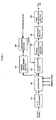
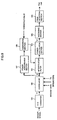
- Fig. 1 is a block diagram of a reception timing detection circuit of a CDMA receiver of a first embodiment of the present invention.
- the reception timing detection circuit of the CDMA receiver comprises an A/D converter 101 for converting a reception signal into a digital reception signal S, a correlator 102 for obtaining a cross-correlation between the digital reception signal S and a known signal series periodically within a predetermined lag (within a delay period), an interpolation filter 103 for re-sampling an output signal R of the correlator 102 at a frequency higher than the sampling frequency of the A/D converter 101, a power calculation section 104 for obtaining the cross-correlation signal power P that has been re-sampled at the interpolation filter 103, an averaging section 105 for averaging the cross-correlation signal power P over a plurality of cycles and a peak detection section 106 for obtaining a peak Popt of the cross-correlation signal power P that has been averaged by the averaging section 105 and determining an optimum reception timing ⁇ opt.
- the transmission/reception signal that reduces power leaking from the band is band limited with a raised cosine filter exhibiting a roll off factor ranging from 10 to 50%.
- the frequency bandwidth of the transmission/reception signal is kept to be 1.1 to 1.5 times more than the chip rate.
- the sampling frequency for the A/D converter 101 should be at least twice the chip rate.
- the in-phase component (I component) and orthogonal component (Q component) of the complex base band signal are A/D converted, respectively to obtain the digital reception signal S.
- the thus obtained digital reception signal S is expressed as a complex number comprising the in-phase component as a real number section and the orthogonal component as an imaginary number section.
- the digital reception signal S obtained through A/D conversion with an I/F signal at a sampling frequency four times higher than the chip rate also has an equivalent value.
- the sampling frequency is the minimum frequency shared by the data demodulation section. Accordingly any further higher frequency can be used for sampling. It is also possible that a correlation is obtained through the analogue circuit and then the output signal of the correlator 102 is A/D converted at the aforementioned sampling frequency.
- Fig. 2 is a time chart representing the respective formats of a transmission signal and a spread code received by the CDMA receiver of Fig. 1 as the reception signal.
- the transmission signal has an L symbol equivalent to 1 slot.
- the Np symbol as the pilot symbol (PL : known code) is inserted to the head of each slot.
- the spreading ratio (the number of chips of the spread code per symbol) is referred to as M.
- the correlator 102 obtains the cross-correlation value Rn( ⁇ ) at the nth slot using the following equation.
- the mobile station is basically expected to return the up link signal synchronized with the downlink signal from the base station. Accordingly the reception timing is readily predictable for the receiver of the base station. Dispersion of the reception timing is observed in the propagation delay time dependent upon the distance between the base station and the mobile station and synchronous accuracy of the uplink and downlink signals of the mobile unit.
- the wideband system representative of the CDMA method (for example, ranging from 1MHz to 20MHz) is likely to be affected by the propagation delay time rather than the synchronous accuracy of the mobile unit.
- the maximum propagation time can be derived from the time taken for the wave to run between the maximum cell radius covered by a certain base station.
- the minimum value ⁇ min of the delay range Tw can be derived from subtracting a margin from the delay within the receiver by setting the propagation delay to zero.
- the maximum value ⁇ max of the delay range Tw can be derived from adding the margin to the delay within the receiver to the maximum value of the propagation delay.
- the delay range Tw cannot be obtained in the above manner from the beginning. After synchronizing the clock with the base station by completing the initial synchronization, the delay range can be restricted in the similar manner so that the propagation delay is considered.
- the interpolation filter 103 interpolates a correlation value between 2 samples per chip output from the series cross-correlator 102 so as to calculate the correlation value with higher delay accuracy. It is required to obtain the correlation value at an interval of 1/4 to 1/16 chip conforming to the allowable timing detection difference and sensitivity deterioration.
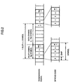
- Fig. 3A The example for obtaining the cross-correlation value with the accuracy of 1/8 chip is described referring to Fig. 3A to 3C.
- Three zeros are inserted between the cross-correlation values at an interval of 1/2 chip (Fig. 3A) output from the correlator 102, respectively so that the signal series at an interval of 1/8 chip is generated (see Fig. 3B).
- the series at an interval of 1/8 chip is subjected to filtering through a low pass filter (LPF) at cut off frequency identical to the chip rate, thus presenting the cross-correlated series having interpolation at each 1/8 chip interval (Fig. 3C).
- LPF low pass filter
- the above impulse response may have a limitless length. Practically it can be restricted to range from +/-1 chip to +/-8 chip by providing a window, allowing for the use of FIR filter.
- the impulse response is restricted to +/- 2 chip, the number of taps of the FIR filter becomes 16 ((8 samples/chip) x 4 chips). As 3 out of 4 samples of the input signal are preliminarily set to zero, adding operation required for calculating the output of 1 sample is executed only 8 times.
- the adding operation has to be executed Np x M times per cross-correlation value of 1 sample.
- the calculation for obtaining the correlation is executed once at 4 samples.
- the delay time when the cross-correlation value takes the peak is ultimately required for the output of the reception timing detection circuit.
- the interpolation filter does not have to execute.high accurate calculation for obtaining the delay time in the section where the cross-correlation power value is small. That is, the interpolation filter is so controlled not to operate in the section where the cross-correlation power value is smaller than a predetermined threshold value so as to reduce the calculation amount that should be done by the interpolation filter.
- the threshold value governing ON/OFF of the interpolation filter is decided by noise power and peak power of the predicted cross-correlation value as well as the calculation amount required to be reduced and the critical ratio causing detection failure owing to a peak error.
- the threshold can be set to a value smaller than 1/10 of the peak power expected to be twice the noise power.
- a power measurement section 107 measures power of an output R of the correlator 102. Then a comparison section 108 compares the measured power with the threshold value decided as described above. The comparison section 108 outputs a signal for stopping the operation of the interpolation filter 103 in the section where the cross-correlation power value is smaller than the threshold value. Upon receiving the stop signal, the interpolation filter 103 outputs an output R of the correlator 102 as it has been input.
- the phase of the reception signal may become gradually shifted between slots. It is thus impossible to improve Eb/No through in-phase combine that has been applied to the adjacent pilot symbols. So the phase component is removed by obtaining power of the correlation (sum of squares of the I component and Q component) in the power calculation section 104 and then the cross-correlation values between slots within the same delay time period are averaged by the averaging section 105.
- the aforementioned averaging is executed in order to average dispersion owing to noise and variation owing to fading. Taking a large number of averaged slots may reduce dispersion owing to noise. However, the speed for tracking shadowing is decreased. Therefore it is preferable to keep the number of the averaged slots as minimum as possible. In case of a large number of pilot symbols (for example, 16), averaging is not necessarily required.
- the average value can be obtained in several different ways, for example, by splitting into blocks at every predetermined number of slots, obtaining the mobile average through sliding, or obtaining an index weighted mean value.
- Pave n ( ⁇ ) ⁇ ⁇ Pave n ( ⁇ ) + (1 - ⁇ ) ⁇ Pn ( ⁇ ).
- the peak detection circuit 106 obtains the delay times ⁇ opt at which the averaged cross-correlation power Pave n( ⁇ ) takes a.maximum value. If the data reception section (not shown) is formed as a RAKE receiver that can combine a plurality of multiple paths in maximum ratio, the peak detection circuit 106 obtains the number of peaks equivalent to that of the RAKE fingers in order of larger size for outputting the delay time ⁇ opt.
- Fig. 4 is a block diagram of an example of the correlator 102 shown in Fig. 1.
- the correlator 102 comprises a matched filter 201 and a time window section 202.
- the matched filter 201 is the filter matched with the series obtained by spreading the pilot symbol with the spread code. More specifically, it is realized by a FIR filter, taking the complex conjugate series of the aforementioned series as the tap coefficient.
- the time window section 202 selectively allows only a cross-correlation value of the predetermined delay time range Tw to pass through.
- Fig. 5 is a block diagram of another example of the correlator 102 shown in Fig. 1.
- the circuit shown in Fig. 5 is effective only when the spread code length is equivalent to 1 symbol time of the pilot symbol. This type of circuit reduces the operation amount required for cross-correlation compared with the conventional circuit having the spread code length longer than 1 symbol.
- the correlator 102 comprises a first memory 301 of serial input parallel output type for storing a digital reception signal S for a time period obtained by adding 1 symbol time length of the pilot symbol to the time length of a predetermined delay range, an demodulation section 302 for demodulating the parallel output of the first memory 301 according to the pilot symbol code, an coherent adder section 306 provided with an adder 303 and a memory 304 for coherent adding the demodulated digital reception signal over a plurality of pilot symbols and a correlator 305 for obtaining a cross-correlation between the coherent added digital reception signal and the spread code within a predetermined delay range Tw.
- the size of the first memory 301 is 4M.
- the demodulation circuit 302 multiplies a complex conjugate number of the mth pilot symbol PL(m) at the nth slot with all the above 4M samples.
- the coherent adder 306 accumulation adds each 4M sample output from the demodulation circuit 302 to all Np pilot symbols.
- the head of the slot is cleared to zero and no addition is executed over the slots.
- Fig. 6 is a block diagram of another example of the correlator 102 shown in Fig. 1.
- the correlator 102 comprises a first memory 401 for storing a digital reception signal S for a period obtained by adding a time length of the pilot symbol series to a predetermined time length of the delay range Tw, a second memory 406 for storing a spread code c corresponding to a pilot symbol PL, a correlator 402 for obtaining a cross-correlation per symbol by reading the digital reception signal S and the spread code from the first memory 401 and the second memory 406, respectively , an demodulation section 403 for demodulating the cross-correlation value output from the correlator 402 conforming to the pilot symbol PL, an coherent adder section 404 for accumulation adding the demodulated correlation signals over a plurality of pilot symbols, and a timing control section 405 for controlling the reception timing so that the pilot symbol is contained in the digital reception signal S accumulated in the first memory 401 and controlling to read from the first memory 401 and the second memory 406 repeatedly by sliding the timing until all cross-correlations
- Fig. 7 is a block diagram of a further example of the correlator 102 shown in Fig. 1.
- this correlator 102 comprises a first memory 501 for storing a digital reception signal S for a period obtained by adding a time length of the pilot symbol series to a time length of a predetermined delay range Tw, a spread section 504 for spreading the pilot symbol PL with a spread code, a second memory 505 for storing the pilot symbol spread by the spread section 504, a correlator 502 for obtaining a cross-correlation by reading the digital reception signal S and the spread pilot symbol from the first memory 501 and the second memory 505, respectively and a timing control section 503 for controlling the reception timing so that the pilot symbol is contained in the digital reception signal S accumulated in the first memory 501 and controlling to read from the first memory 501 and the second memory 505 repeatedly by sliding the timing until all cross-correlations are obtained within the predetermined delay range Tw.
- Each of the correlators 102 shown in Fig. 6 and Fig. 7 is the circuit that can be applied when the spread code has a longer symbol time length, i.e., direct spread using a long code, than 1 symbol time. length of the pilot symbol.
- the correlation between the reception data and the spread code is obtained (de-spread) in the same manner as normal data reception and demodulation is executed using a known pilot symbol. Then coherent adding is executed by removing the demodulation component.
- the series in which the pilot symbol is preliminarily spread is obtained and the cross-correlation between the known series and the reception signal is directly obtained.
- the method shown in Fig. 6 can provide the correlation value at every symbol as the result of the middle of the process.
- the circuit shown in Fig. 7 should be better choice because of its simple construction.
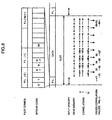
- Fig. 8 is a time chart showing the operation of the correlator 102 shown in Fig. 7.
- Fig. 8 represents that the correlator 502 parallel calculates to obtain the cross-correlation with respect to 32 delay times.
- the number of parallel calculations that can be done is defined by a trade-off, relationship between the hardware size and the cross-correlation operation time. Therefore an optimum number can be decided by considering the spreading ratio, delay time range for searching the peak, slot cycle, process clock rate and the like.
- 32 units of parallel correlators are used to obtain 4M cross-correlation values.
- the reception signal and the spread pilot symbol series are read from the memories repeatedly 4M/32 times for executing correlation operation.
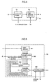
- the reception timing detection circuit of the CDMA receiver processes decided data obtained by deciding reception data of a reception signal as a known signal instead of using the pilot symbol. That is, the reception timing detection circuit of the CDMA receiver shown in Fig. 9 is identical to the reception timing detection circuit of the CDMA receiver as shown in Fig. 1 except that the known signal input to the correlator 102 is not the pilot symbol but the decided data.
- Fig. 10 is a block diagram of a CDMA receiver comprising the reception timing detection circuit shown in Fig. 1.
- the CDMA receiver comprises the correlator 102 as shown in Fig. 7.
- the CDMA receiver comprises a radio reception section 602 for converting a radio signal received via an antenna 601 into a complex base band signal.
- An A/D converter 101 digitizes the complex base band signal into a digital reception signal.
- a first memory 501 stores the digital reception signal.
- a spread section 504 spreads the pilot symbol PL with a spread code.
- a second memory 505 stores the spread pilot symbol series.
- a correlator 502 reads the digital reception signal and the spread pilot symbol from the first memory 501 and the second memory 505, respectively for obtaining a cross-correlation.
- a power calculation section 104 calculates power of the cross-correlation series that has been interpolated by an interpolation filter 103 as the cross-correlation power.
- An averaging section 105 averages the cross-correlation power within the same delay time over a plurality of slots.
- a peak detection section 106 detects a peak of the averaged cross-correlation power.
- a timing control section 503 controls the respective operation timings.of the first and the second memories 501 and 505, correlator 502, interpolation filter 103, power calculation section 104, averaging section 105 and peak detection section 106.
- a spread code generation section 603 generates a spread code and supplies the spread code to the spread section 504 and an de-spread section 605.
- the de-spread section 605 outputs a de-spread data signal by multiplying a complex conjugate of the spread code by the digital reception signal and integrating the multiplication result by 1 symbol.
- a pilot symbol assisted coherent detection section 606 obtains a reference phase at each symbol timing within the slot through straight interpolation, taking a known pilot symbol inserted to the head of 2 successive slots as a reference signal for coherent detection.
- Fig. 11 is a block diagram of another example of the CDMA receiver that realizes the same function as performed by the CDMA receiver as shown in Fig. 10.
- the CDMA receiver comprises the identical elements to those designated as the same reference numerals.
- the CDMA receiver comprises a searcher correlator 705 for storing a correlation series between the digital reception signal and the spread pilot symbol series at each slot in a 2 port RAM 706, a RAM 704 for temporarily storing reception data used by the searcher correlator 705, a spread code generator 708 for generating a spread code and a spread pilot symbol series and supplying them to the searcher correlator 705 and the data demodulation correlator 709, a data demodulation correlator 709 for de-spreading a digital signal to a plurality of multiple path signals with a plurality of RAKE fingers in accordance with a reception delay ordered by a DSP (digital signal processor) 707 and storing the de-spread signal in the 2 port RAM 710 and the DSP 707 for setting an optimum reception timing in the spread code generator 708 by detecting the peak of the cross-correlation series stored in the
- DSP
- the searcher correlator 705, spread code generator 708 and data demodulation correlator 709 can be formed by a hardware, for example, gate array (G/A), exclusive LSI, and the like. Assuming that the chip rate is set to 4.096 Mcps and the symbol rate to 256 ksps, the exclusive hardware may process the chip rate requiring simple and high-rate processing. The DSP firmware, however, may realize symbol rate processing requiring a relatively low rate but complex processing. As a result, the most desirable embodiment can be realized.
- G/A gate array
- exclusive LSI exclusive LSI
- a first advantageous effect of the present invention is that the probability and accuracy for appropriately detecting the peak point of the delay profile can be improved even if the Eb/No per path is low. Therefore the appropriate reception timing can be always established, leading to the improved reception quality. Furthermore, as the present invention meets desired reception quality even under the lower Eb/No condition, the capacity of the cellular system using the CDMA and the cell radius covered by 1 base station can be enlarged.
- the present invention can completely solve such problem that the cross-correlation value obtained at a moment when the reception level is raised by fading exceeds the cross-correlation value of the correct peak point obtained at a moment when the reception level is low.
- the cross-correlation value is obtained at 1/2 chip interval and then it is obtained at a shorter interval using an interpolation filter. Accordingly more accurate peak point (delay time) of the delay profile can be obtained.
- the present invention greatly improves the accuracy of detecting the reception timing without increasing processing amount.
- a second advantageous effect of the present invention is that the operation amount required for obtaining the peak of the delay profile can be reduced.
- the present invention requires to obtain the correlation value only at 1/2 interval in order to keep deterioration of the Eb/No required to an optimum reception timing to be 1dB or less.
- the prior art requires to obtain power of the correlation value at 1/4 interval. Since the noise contained in the cross-correlation value can be reduced, the number of averaging processings for restraining the dispersion of the noise power can also be decreased.
- a third advantageous effect of the present invention is that the size of the hardware used for the base station system can be reduced.
- the power measurement section 107 and comparison section 108 are provided and the interpolation filter 103 is operated at a predetermined threshold value or more.
- the objective of the present invention can be achieved by operating the interpolation filter 103 irrespective of the threshold value under no provision of the power measurement section 107 and comparison section 108.
Description
- The present invention relates to a transmitter/receiver of a mobile communication system, especially an automobile phone/handy phone system (cellular system) using a direct spread code division multiple access (DS-CDMA) system and, more particularly, to a reception timing detection circuit of a receiver used in a base station.
- Among many mobile communication systems, North America Standard system (TIA IS95) using a code division multiple access (CDMA) method is well known as the digital automobile phone/handy phone system (cellular system). The standard specification TIA/EIA/IS (INTERIM STANDARD) titled "Mobile Station - Base Station Compatibility Standard for Dual-Mode Wideband Spread Spectrum Cellular System PN-3421" was published on May, 1994 by TIA (Telecommunication Industry Association). The above specification describes the required operation of the mobile station in Chapter 6 of 95-A and the required operation of the base station in Chapter 7. This standard specification mainly aims at standardizing radio interface by specifying modulation method, signal format and the like. However the exact reception method is not specified in detail.
- On the downlink channel from the base station to the mobile station, common pilot channel (PLCH) not data modulated is transmitted using relatively high power in addition to data modulated traffic channel (TCH) of a plurality of users. The mobile station is able to decide the optimum reception timing using the pilot channel. Therefore determination of the reception timing under a low Eb/No (the ratio of noise power per Hz to signal power per bit) condition is considered as a minor problem. In order to transmit the pilot channel using high power, the number of traffic channels through which data are actually transmitted has to be reduced. This leads to decrease the number of users per base station.
- The uplink channel of IS-95-A from the mobile station to the base station employs a modulation method as a combination of modulation and 4 times direct spread using 64-ary orthogonal code and no common pilot channel thereon. Using the 64-ary orthogonal code allows for enhancing power per symbol compared with BPSK, QPSK and the like and prevents deterioration accompanied with coherent detection in spite of using a coherent detection. This results in, however, complicated reception method.
- Main items of the IS-95-A are:
- chip rate : 1.2288Mcps;
- bit rate : 9.6kbps; and
- spreading ratio of direct spread : 128 times.
-
- The chip rate is relatively low and chip cycle is relatively longer than that of instantaneous variable amplitude of propagation delay. Therefore the reception characteristics are hardly susceptible to the effect of insufficient characteristics of the reception timing detection circuit. However, both bit rate and chip rate have to be accelerated at least 5 to 10 times higher for executing high-rate data communication as well as voice data. This problem has never been posed by the IS-95-A.
- The conventional reception timing detection method (chip synchronization) is described in the document titled "Principle of Spread Spectrum Communication" written by Andrew J. Viterbi, published on April, 1995, Chapter 3, pp. 39-66. The signal that has been spread with a spread code as pseudo random code is captured at two phases, initial searching synchronous and tracking synchronous .
- In the initial searching synchronous method, serial search is executed by sliding the reception timing by 1/2 chip interval until the correlation power exceeds a given threshold value as described in Chapter 3, section 4 of the above document.
- In the tracking synchronous method, called as "early-late gate" or "delay lock loop" (DLL), the timing is finely adjusted by obtaining the correlation power at the timing ahead the reception delay time by Δt and the correlation power at the timing behind the reception delay time by Δt so as to make the difference zero.
- A publication of JP-A 34794/1992 discloses the method in which the above-described initial searching synchronous and tracking synchronous methods are improved, the circuit is shared and the function for tracking the multiple propagation paths is added. The basic operation of this method is identical to that of the reference as described above, failing to solve the task of the IS-95-A.
- The code division multiple access (CDMA) method realizes communication that satisfies quality requirement under a very low Eb/No condition by employing such technologies as path diversity using multiple path propagation (RAKE), macro diversity for connecting a plurality of base stations around the cell boundary (soft hand off), error correction code exhibiting high encoding gain, transmission power control and the like.
- The CDMA method requires strict synchronization of chip timing for reception. If the number of diversity branches (the number of paths) increases, the correct path timing has to be detected under a very low Eb/No condition per path.
- In the conventional method for obtaining a correlation value by sliding a correlation timing and detecting the timing when the correlation power becomes maximum, especially when the noise power is higher than the signal power, failure in peak detection frequently occurs owing to noise. This is the first problem of the conventional art.
- The power of the correlation per symbol is obtained by summing the signal power and the noise power. When the correlation power value is averaged over a plurality of symbols, dispersion of the measured correlation values is decreased. However, the original correlation peak is too small to detect the right peak. This is the first reason.
- In the conventional method, the reception signal does not always coincide with the one that has been used for calculating the correlation value with different delays. In case the reception level varies to the greatest degree owing to fading, the peak of the sliding correlation value does not always coincide with the peak of the right delay profile. This is the second reason.
- In order to obtain the peak of the delay profile accurately, the conventional method requires a large amount of correlation operation. This is the second problem that should be solved.
- The conventional method obtains power of the correlation values and further the average value of the obtained power. As the process for obtaining the power contains a square operation (non-linear operation), linearity is no longer retained, allowing for no interpolation of the delay profile. Therefore, the correlation value has to be calculated by changing the delay time with the intended accuracy.
- As the third problem, the conventional method requires a large sized hardware.
- More specifically, two types of circuits, initial searching synchronization circuit (search circuit) and tracking synchronization circuit (for example, delay lock loop: DLL) are required to cope with the change in the propagation condition resulted from the initial timing capture, secondary synchronization capture after getting off the synchronization, shadowing, or the like, resulting in an enlarged hardware.
- It is an objective of the present invention to provide a reception timing detection circuit of a CDMA receiver of a mobile communication system employing a code division multiple access (CDMA) method, allowing for obtaining the delay profile with high accuracy under a low Eb/No environment condition, requiring least calculation amount, thus improving reception quality of the CDMA receiver and saving power consumption.
- The present invention provides a reception timing detection circuit of a CDMA receiver used for a mobile communication system using a direct spread code division multiple access method comprising correlation means for obtaining a cross-correlation between a reception signal and a known signal series periodically within a predetermined lag and outputting a cross-correlation signal indicating said obtained cross-correlation, an interpolation filter for re-sampling said cross-correlation signal at a frequency higher than a sampling frequency for said cross-correlation signal and outputting said re-sampled cross-correlation signal, power calculation means for calculating power of said re-sampled cross-correlation signal, averaging means for averaging said calculated power of cross-correlation signal over a plurality of cycles and peak detection means for detecting a peak of said averaged power of cross-correlation signal and determining a timing at which said peak is detected as a reception timing.
- The present invention obtains a cross-correlation between a reception signal and a known signal series comprising a plurality of symbols so as to decrease the power of noise component contained in the cross-correlation power.
- . The cross-correlation is obtained at the minimum number of sampling frequency selected from the frequency bandwidth of the transmission/reception signal. The obtained cross-correlation value is interpolated through an interpolation filter so that cross-correlation power, i.e., peak of the delay profile is detected with a desired delay accuracy. Therefore the operation amount required for obtaining the cross-correlation can be reduced. Since the present invention uses the same reception signal for calculating all the cross-correlation values, the correlation value never varies accompanied with variation of the reception level due to fading.
- This and other objectives, features and advantages of the present invention will become more apparent upon a reading of the following detailed description and drawings, in which:
- Fig. 1 is a block diagram of a reception timing detection circuit of a CDMA receiver of a first embodiment of the present invention;
- Fig. 2 is a time chart representing each format of a transmission signal and a spread code received by the reception timing detection circuit of the CDMA receiver shown in Fig. 1 as a reception signal;
- Fig. 3A to 3C are time charts representing an operation of an interpolation filter of the reception timing detection circuit of the CDMA receiver shown in Fig. 1;
- Fig. 4 is a block diagram of an example of a correlator of the reception timing detection circuit of the CDMA receiver shown in Fig. 1;
- Fig. 5 is a block diagram of another example of a correlator of the reception timing detection circuit of the CDMA receiver shown in Fig. 1;
- Fig. 6 is a block diagram of other example of a correlator of the reception timing detection circuit of the CDMA receiver shown in Fig. 1;
- Fig. 7 is a block diagram of a still further example of a correlator of the reception timing detection circuit of the CDMA receiver shown in Fig. 1;
- Fig. 8 is a time chart representing an operation of the correlator shown in Fig. 7;
- Fig. 9 is a block diagram of a reception timing detection circuit of a CDMA receiver of a second embodiment of the present invention;
- Fig. 10 is a block diagram of the CDMA receiver comprising the reception timing detection circuit shown in Fig. 1; and
- Fig. 11 is a block diagram of another type of the CDMA receiver that realizes the same function performed by the CDMA receiver shown in Fig. 10.
-
- Embodiments of the present invention are described referring to the drawings.
- Fig. 1 is a block diagram of a reception timing detection circuit of a CDMA receiver of a first embodiment of the present invention.
- Referring to Fig. 1, the reception timing detection circuit of the CDMA receiver comprises an A/
D converter 101 for converting a reception signal into a digital reception signal S, acorrelator 102 for obtaining a cross-correlation between the digital reception signal S and a known signal series periodically within a predetermined lag (within a delay period), aninterpolation filter 103 for re-sampling an output signal R of thecorrelator 102 at a frequency higher than the sampling frequency of the A/D converter 101, apower calculation section 104 for obtaining the cross-correlation signal power P that has been re-sampled at theinterpolation filter 103, anaveraging section 105 for averaging the cross-correlation signal power P over a plurality of cycles and apeak detection section 106 for obtaining a peak Popt of the cross-correlation signal power P that has been averaged by the averagingsection 105 and determining an optimum reception timing τopt. - The transmission/reception signal that reduces power leaking from the band is band limited with a raised cosine filter exhibiting a roll off factor ranging from 10 to 50%. In this case, the frequency bandwidth of the transmission/reception signal is kept to be 1.1 to 1.5 times more than the chip rate. When digitizing a radio band signal that has been converted into a complex base band signal, the sampling frequency for the A/
D converter 101 should be at least twice the chip rate. The in-phase component (I component) and orthogonal component (Q component) of the complex base band signal are A/D converted, respectively to obtain the digital reception signal S. The thus obtained digital reception signal S is expressed as a complex number comprising the in-phase component as a real number section and the orthogonal component as an imaginary number section. The digital reception signal S obtained through A/D conversion with an I/F signal at a sampling frequency four times higher than the chip rate also has an equivalent value. - The sampling frequency, as the most effective feature of the present invention, is the minimum frequency shared by the data demodulation section. Accordingly any further higher frequency can be used for sampling. It is also possible that a correlation is obtained through the analogue circuit and then the output signal of the
correlator 102 is A/D converted at the aforementioned sampling frequency. - Fig. 2 is a time chart representing the respective formats of a transmission signal and a spread code received by the CDMA receiver of Fig. 1 as the reception signal.
- Referring to Fig. 1 and Fig. 2, the transmission signal has an L symbol equivalent to 1 slot. The Np symbol as the pilot symbol (PL : known code) is inserted to the head of each slot. The spreading ratio (the number of chips of the spread code per symbol) is referred to as M.
- The
correlator 102 obtains the cross-correlation value Rn(τ) at the nth slot using the following equation. - Supposing that the known signal series at the nth slot is Pn(i), the known signal length N = Np x M chip, sampling frequency twice the chip rate used for the reception signal, the period for obtaining the cross-correlation (delay range) Tw is τmin to τmax, the following equation is established:
- The delay range Tw = τmin ∼ τmax used for obtaining the correlation can be decided as described below. In the cellular system for communication between the base station and mobile station, especially the mobile station is basically expected to return the up link signal synchronized with the downlink signal from the base station. Accordingly the reception timing is readily predictable for the receiver of the base station. Dispersion of the reception timing is observed in the propagation delay time dependent upon the distance between the base station and the mobile station and synchronous accuracy of the uplink and downlink signals of the mobile unit. The wideband system representative of the CDMA method (for example, ranging from 1MHz to 20MHz) is likely to be affected by the propagation delay time rather than the synchronous accuracy of the mobile unit. The maximum propagation time can be derived from the time taken for the wave to run between the maximum cell radius covered by a certain base station. In the receiver of the base station, the minimum value τmin of the delay range Tw can be derived from subtracting a margin from the delay within the receiver by setting the propagation delay to zero. The maximum value τmax of the delay range Tw can be derived from adding the margin to the delay within the receiver to the maximum value of the propagation delay. In the mobile unit, however, the delay range Tw cannot be obtained in the above manner from the beginning. After synchronizing the clock with the base station by completing the initial synchronization, the delay range can be restricted in the similar manner so that the propagation delay is considered.
- The
interpolation filter 103 interpolates a correlation value between 2 samples per chip output from theseries cross-correlator 102 so as to calculate the correlation value with higher delay accuracy. It is required to obtain the correlation value at an interval of 1/4 to 1/16 chip conforming to the allowable timing detection difference and sensitivity deterioration. - The example for obtaining the cross-correlation value with the accuracy of 1/8 chip is described referring to Fig. 3A to 3C. Three zeros are inserted between the cross-correlation values at an interval of 1/2 chip (Fig. 3A) output from the
correlator 102, respectively so that the signal series at an interval of 1/8 chip is generated (see Fig. 3B). The series at an interval of 1/8 chip is subjected to filtering through a low pass filter (LPF) at cut off frequency identical to the chip rate, thus presenting the cross-correlated series having interpolation at each 1/8 chip interval (Fig. 3C). The impulse response of the LPF can be expressed by the following equation: - The above impulse response may have a limitless length. Practically it can be restricted to range from +/-1 chip to +/-8 chip by providing a window, allowing for the use of FIR filter. When the impulse response is restricted to +/- 2 chip, the number of taps of the FIR filter becomes 16 ((8 samples/chip) x 4 chips). As 3 out of 4 samples of the input signal are preliminarily set to zero, adding operation required for calculating the output of 1 sample is executed only 8 times.
- In the conventional method without using the interpolation filter to obtain the cross-correlation with 1/8 chip accuracy, the adding operation has to be executed Np x M times per cross-correlation value of 1 sample. In the present embodiment, however, the calculation for obtaining the correlation is executed once at 4 samples. As for the rest of 3 times, only 8 times of adding operation are required as described above. Therefore the number of required adding operations is defined by the following equation:
- Normally as it is obvious that M (spreading ratio) >>1, the operation amount can be reduced by about 1/4 compared with the conventional method.
- The delay time when the cross-correlation value takes the peak is ultimately required for the output of the reception timing detection circuit. When all the cross-correlation values in the short section corresponding to the impulse response time of the interpolation filter are small, a large signal is never output from the interpolation filter. Therefore the interpolation filter does not have to execute.high accurate calculation for obtaining the delay time in the section where the cross-correlation power value is small. That is, the interpolation filter is so controlled not to operate in the section where the cross-correlation power value is smaller than a predetermined threshold value so as to reduce the calculation amount that should be done by the interpolation filter. The threshold value governing ON/OFF of the interpolation filter is decided by noise power and peak power of the predicted cross-correlation value as well as the calculation amount required to be reduced and the critical ratio causing detection failure owing to a peak error. For example, the threshold can be set to a value smaller than 1/10 of the peak power expected to be twice the noise power.
- In this embodiment, a
power measurement section 107 measures power of an output R of thecorrelator 102. Then acomparison section 108 compares the measured power with the threshold value decided as described above. Thecomparison section 108 outputs a signal for stopping the operation of theinterpolation filter 103 in the section where the cross-correlation power value is smaller than the threshold value. Upon receiving the stop signal, theinterpolation filter 103 outputs an output R of thecorrelator 102 as it has been input. - The phase of the reception signal may become gradually shifted between slots. It is thus impossible to improve Eb/No through in-phase combine that has been applied to the adjacent pilot symbols. So the phase component is removed by obtaining power of the correlation (sum of squares of the I component and Q component) in the
power calculation section 104 and then the cross-correlation values between slots within the same delay time period are averaged by the averagingsection 105. - The aforementioned averaging is executed in order to average dispersion owing to noise and variation owing to fading. Taking a large number of averaged slots may reduce dispersion owing to noise. However, the speed for tracking shadowing is decreased. Therefore it is preferable to keep the number of the averaged slots as minimum as possible. In case of a large number of pilot symbols (for example, 16), averaging is not necessarily required. The average value can be obtained in several different ways, for example, by splitting into blocks at every predetermined number of slots, obtaining the mobile average through sliding, or obtaining an index weighted mean value.
- The cross-correlation power Pn(τ) to the delay τ at the nth slot can be obtained by the following equation:
- When index weighting with an oblivion index λ, the averaged cross-correlation power Pave n (τ) to the delay τ at the nth slot is derived from the following equation:
- The
peak detection circuit 106 obtains the delay times τ opt at which the averaged cross-correlation power Pave n(τ) takes a.maximum value. If the data reception section (not shown) is formed as a RAKE receiver that can combine a plurality of multiple paths in maximum ratio, thepeak detection circuit 106 obtains the number of peaks equivalent to that of the RAKE fingers in order of larger size for outputting the delay time τopt. - Fig. 4 is a block diagram of an example of the
correlator 102 shown in Fig. 1. - Referring to Fig. 4, the
correlator 102 comprises a matchedfilter 201 and atime window section 202. - The matched
filter 201 is the filter matched with the series obtained by spreading the pilot symbol with the spread code. More specifically, it is realized by a FIR filter, taking the complex conjugate series of the aforementioned series as the tap coefficient. - The
time window section 202 selectively allows only a cross-correlation value of the predetermined delay time range Tw to pass through. - Fig. 5 is a block diagram of another example of the
correlator 102 shown in Fig. 1. The circuit shown in Fig. 5 is effective only when the spread code length is equivalent to 1 symbol time of the pilot symbol. This type of circuit reduces the operation amount required for cross-correlation compared with the conventional circuit having the spread code length longer than 1 symbol. - Referring to Fig. 5, the
correlator 102 comprises afirst memory 301 of serial input parallel output type for storing a digital reception signal S for a time period obtained by adding 1 symbol time length of the pilot symbol to the time length of a predetermined delay range, andemodulation section 302 for demodulating the parallel output of thefirst memory 301 according to the pilot symbol code, ancoherent adder section 306 provided with anadder 303 and amemory 304 for coherent adding the demodulated digital reception signal over a plurality of pilot symbols and acorrelator 305 for obtaining a cross-correlation between the coherent added digital reception signal and the spread code within a predetermined delay range Tw. - In order to simplify the explanation how the
correlation 102 shown in Fig. 5 operates, it is assumed that τmin is equivalent to zero and τmax is equivalent to 2M-1 (M chip represents 1 symbol time). - In the above condition, the size of the
first memory 301 is 4M. After receiving a digital reception signal equivalent to 1 symbol time, thefirst memory 301 parallel outputs the reception signal equivalent to the time of last 2 symbols. That is, after receiving the digital reception signal corresponding to the (m+1)th symbol (m = 0 - Np-1) at the nth slot, thefirst memory 301 parallel outputs a digital reception signal for 4M samples obtained by the equation as below: - The
demodulation circuit 302 multiplies a complex conjugate number of the mth pilot symbol PL(m) at the nth slot with all the above 4M samples. - The
coherent adder 306 accumulation adds each 4M sample output from thedemodulation circuit 302 to all Np pilot symbols. The head of the slot is cleared to zero and no addition is executed over the slots. - The coherent added 4M sample is obtained by the following equation;
- The
correlator 305 calculates the coherent added signal Save (i) ; i=0∼4M-1 and cross-correlation of the spread code series c(i) ; i=0∼M-1 within the delay time τ=0∼2M-1. - The correlation Rn(τ) is obtained by the following equation:
- The number of adding operations required for obtaining the cross-correlation in the range of τ=0∼2M-1 is 4M x Np + 2M2. Increasing the number of the pilot symbols Np can reduce the number of the above adding operations.
- Fig. 6 is a block diagram of another example of the
correlator 102 shown in Fig. 1. - Referring to Fig. 6, the
correlator 102 comprises afirst memory 401 for storing a digital reception signal S for a period obtained by adding a time length of the pilot symbol series to a predetermined time length of the delay range Tw, asecond memory 406 for storing a spread code c corresponding to a pilot symbol PL, acorrelator 402 for obtaining a cross-correlation per symbol by reading the digital reception signal S and the spread code from thefirst memory 401 and thesecond memory 406, respectively , andemodulation section 403 for demodulating the cross-correlation value output from thecorrelator 402 conforming to the pilot symbol PL, ancoherent adder section 404 for accumulation adding the demodulated correlation signals over a plurality of pilot symbols, and atiming control section 405 for controlling the reception timing so that the pilot symbol is contained in the digital reception signal S accumulated in thefirst memory 401 and controlling to read from thefirst memory 401 and thesecond memory 406 repeatedly by sliding the timing until all cross-correlations are obtained within the predetermined delay range Tw. - Fig. 7 is a block diagram of a further example of the
correlator 102 shown in Fig. 1. - Referring to Fig. 7, this
correlator 102 comprises afirst memory 501 for storing a digital reception signal S for a period obtained by adding a time length of the pilot symbol series to a time length of a predetermined delay range Tw, aspread section 504 for spreading the pilot symbol PL with a spread code, asecond memory 505 for storing the pilot symbol spread by thespread section 504, acorrelator 502 for obtaining a cross-correlation by reading the digital reception signal S and the spread pilot symbol from thefirst memory 501 and thesecond memory 505, respectively and atiming control section 503 for controlling the reception timing so that the pilot symbol is contained in the digital reception signal S accumulated in thefirst memory 501 and controlling to read from thefirst memory 501 and thesecond memory 505 repeatedly by sliding the timing until all cross-correlations are obtained within the predetermined delay range Tw. - Each of the
correlators 102 shown in Fig. 6 and Fig. 7 is the circuit that can be applied when the spread code has a longer symbol time length, i.e., direct spread using a long code, than 1 symbol time. length of the pilot symbol. In Fig. 6, the correlation between the reception data and the spread code is obtained (de-spread) in the same manner as normal data reception and demodulation is executed using a known pilot symbol. Then coherent adding is executed by removing the demodulation component. In Fig. 7, the series in which the pilot symbol is preliminarily spread is obtained and the cross-correlation between the known series and the reception signal is directly obtained. The method shown in Fig. 6 can provide the correlation value at every symbol as the result of the middle of the process. In order to obtain the cross-correlation series as the objective of the present invention, the circuit shown in Fig. 7 should be better choice because of its simple construction. - The operation of the
correlator 102 shown in Fig.7 is described. - Fig. 8 is a time chart showing the operation of the
correlator 102 shown in Fig. 7. - Referring to Fig. 7 and Fig. 8, after the digital reception signal corresponding to the pilot symbol and the series where the pilot symbol is spread are input in the
first memory 501 and thesecond memory 505, respectively, the data section is repeatedly read during reception so that the cross-correlation operation is executed repeatedly. Fig. 8 represents that thecorrelator 502 parallel calculates to obtain the cross-correlation with respect to 32 delay times. The number of parallel calculations that can be done is defined by a trade-off, relationship between the hardware size and the cross-correlation operation time. Therefore an optimum number can be decided by considering the spreading ratio, delay time range for searching the peak, slot cycle, process clock rate and the like. In this example, 32 units of parallel correlators are used to obtain 4M cross-correlation values. The reception signal and the spread pilot symbol series are read from the memories repeatedly 4M/32 times for executing correlation operation. - Fig. 9 is a block diagram showing a reception timing detection circuit of a CDMA receiver of a second embodiment of the present invention.
- Referring to Fig. 9, the reception timing detection circuit of the CDMA receiver processes decided data obtained by deciding reception data of a reception signal as a known signal instead of using the pilot symbol. That is, the reception timing detection circuit of the CDMA receiver shown in Fig. 9 is identical to the reception timing detection circuit of the CDMA receiver as shown in Fig. 1 except that the known signal input to the
correlator 102 is not the pilot symbol but the decided data. - Fig. 10 is a block diagram of a CDMA receiver comprising the reception timing detection circuit shown in Fig. 1. Referring to Fig. 10, the CDMA receiver comprises the
correlator 102 as shown in Fig. 7. - The CDMA receiver comprises a
radio reception section 602 for converting a radio signal received via anantenna 601 into a complex base band signal. - An A/
D converter 101 digitizes the complex base band signal into a digital reception signal. Afirst memory 501 stores the digital reception signal. Aspread section 504 spreads the pilot symbol PL with a spread code. Asecond memory 505 stores the spread pilot symbol series. Acorrelator 502 reads the digital reception signal and the spread pilot symbol from thefirst memory 501 and thesecond memory 505, respectively for obtaining a cross-correlation. - A
power calculation section 104 calculates power of the cross-correlation series that has been interpolated by aninterpolation filter 103 as the cross-correlation power. Anaveraging section 105 averages the cross-correlation power within the same delay time over a plurality of slots. Apeak detection section 106 detects a peak of the averaged cross-correlation power. - A
timing control section 503 controls the respective operation timings.of the first and thesecond memories correlator 502,interpolation filter 103,power calculation section 104, averagingsection 105 andpeak detection section 106. - A spread
code generation section 603 generates a spread code and supplies the spread code to thespread section 504 and ande-spread section 605. Thede-spread section 605 outputs a de-spread data signal by multiplying a complex conjugate of the spread code by the digital reception signal and integrating the multiplication result by 1 symbol. A pilot symbol assistedcoherent detection section 606 obtains a reference phase at each symbol timing within the slot through straight interpolation, taking a known pilot symbol inserted to the head of 2 successive slots as a reference signal for coherent detection. ARAKE combining section 607 comprising an de-spread section identical to thede-spread section 605 and a plurality of pilot symbol assisted coherent detection sections identical to the pilot symbol assistedcoherent detection section 606 outputs reception data by wave detecting each path of the multiple path transmission channel and combining in a maximum ratio. A sync.protection section 604 monitors errors of an optimum reception timing τopt detected by thepeak detection section 106, the peak power Popt at the optimum reception timing τ opt and a sync. signal contained in the reception data (The known pilot symbol can be used as the sync. signal.) and controls the spreadcode generation section 603 and thetiming control section 503 so that sync. status is maintained. , - Fig. 11 is a block diagram of another example of the CDMA receiver that realizes the same function as performed by the CDMA receiver as shown in Fig. 10.
- Referring to Fig. 11, the CDMA receiver comprises the identical elements to those designated as the same reference numerals. The CDMA receiver comprises a
searcher correlator 705 for storing a correlation series between the digital reception signal and the spread pilot symbol series at each slot in a 2port RAM 706, aRAM 704 for temporarily storing reception data used by thesearcher correlator 705, aspread code generator 708 for generating a spread code and a spread pilot symbol series and supplying them to thesearcher correlator 705 and thedata demodulation correlator 709, adata demodulation correlator 709 for de-spreading a digital signal to a plurality of multiple path signals with a plurality of RAKE fingers in accordance with a reception delay ordered by a DSP (digital signal processor) 707 and storing the de-spread signal in the 2port RAM 710 and theDSP 707 for setting an optimum reception timing in thespread code generator 708 by detecting the peak of the cross-correlation series stored in the 2port RAM 706 by thesearcher correlator 705 with respect to the interpolation filter operation, power calculation, slot-to-slot averaging and the number of RAKE fingers and reading the de-spread signal written in the 2 port RAM by thedata demodulation correlator 709, combining at a maximum ratio (RAKE combination) by pilot symbol assisted coherent detecting the respective RAKE fingers and then deciding the reception data. - The
searcher correlator 705, spreadcode generator 708 anddata demodulation correlator 709 can be formed by a hardware, for example, gate array (G/A), exclusive LSI, and the like. Assuming that the chip rate is set to 4.096 Mcps and the symbol rate to 256 ksps, the exclusive hardware may process the chip rate requiring simple and high-rate processing. The DSP firmware, however, may realize symbol rate processing requiring a relatively low rate but complex processing. As a result, the most desirable embodiment can be realized. - A first advantageous effect of the present invention is that the probability and accuracy for appropriately detecting the peak point of the delay profile can be improved even if the Eb/No per path is low. Therefore the appropriate reception timing can be always established, leading to the improved reception quality. Furthermore, as the present invention meets desired reception quality even under the lower Eb/No condition, the capacity of the cellular system using the CDMA and the cell radius covered by 1 base station can be enlarged.
- As the first reason for the above-described effect provided by the present invention, the delay profile is provided by obtaining a cross-correlation between a known signal and the reception signal over a plurality of symbols or coherent adding over a plurality of symbols (normally the number of pilot symbols per slot). And then the power (sum of squares) is obtained. As a result, the power of the noise component contained in the cross-correlation value is reduced to 1/(number of pilot symbols), which is smaller than that of the prior art case. Assuming that the number of the pilot symbols per slot is 16, the power of the noise component can be reduced by about 12dB.
- As the second reason, since the same reception signal is repeatedly used for calculating the correlation value with different delays, the level relationship among cross-correlation values with different delays can be strictly maintained irrespective of large variation of the reception level owing to fading. Therefore, the present invention can completely solve such problem that the cross-correlation value obtained at a moment when the reception level is raised by fading exceeds the cross-correlation value of the correct peak point obtained at a moment when the reception level is low.
- As the third reason, in the present invention, the cross-correlation value is obtained at 1/2 chip interval and then it is obtained at a shorter interval using an interpolation filter. Accordingly more accurate peak point (delay time) of the delay profile can be obtained. The present invention greatly improves the accuracy of detecting the reception timing without increasing processing amount.
- A second advantageous effect of the present invention is that the operation amount required for obtaining the peak of the delay profile can be reduced.
- This is because that the present invention requires to obtain the correlation value only at 1/2 interval in order to keep deterioration of the Eb/No required to an optimum reception timing to be 1dB or less. In contrast the prior art requires to obtain power of the correlation value at 1/4 interval. Since the noise contained in the cross-correlation value can be reduced, the number of averaging processings for restraining the dispersion of the noise power can also be decreased.
- A third advantageous effect of the present invention is that the size of the hardware used for the base station system can be reduced.
- This is because that as the circuit of the present invention realizes all functions of the initial sync. capture (initial search), new path capture (search) and sync. tracking by replacing two circuits, initial sync. capture circuit (search circuit) and sync. tracking circuit (for example, DLL (Delay Lock Loop)) that have been required to be equipped with the conventional system.
- Referring to Fig.1 and Fig.9, the
power measurement section 107 andcomparison section 108 are provided and theinterpolation filter 103 is operated at a predetermined threshold value or more. However the objective of the present invention can be achieved by operating theinterpolation filter 103 irrespective of the threshold value under no provision of thepower measurement section 107 andcomparison section 108.
Claims (16)
- A reception timing detection circuit of a CDMA receiver used for a mobile communication system using a direct spread code division multiple access method comprising:correlation means (102) for obtaining a cross-correlation between a reception signal and a known signal series periodically within a predetermined lag and outputting a cross-correlation signal indicating said obtained cross-correlation;an interpolation filter (103) for re-sampling said cross-correlation signal at a frequency higher than a sampling frequency for said cross-correlation signal and outputting said re-sampled cross-correlation signal;power calculation means (104) for calculating power of said re-sampled cross-correlation signal;averaging means (105) for averaging said calculated power of cross-correlation signal over a plurality of cycles; andpeak detection means (106) for detecting a peak of said averaged power of cross-correlation signal and determining a timing at which said peak is detected as a reception timing.
- The reception timing detection circuit of a CDMA receiver of claim 1, wherein said known signal series is obtained by spreading a known pilot symbol inserted to said reception signal at predetermined period with a spread code.
- The reception timing detection circuit of a CDMA receiver of claim 1, wherein said known signal series is obtained by re-spreading a signal series produced by de-spreading said reception signal with a spread code.
- The reception timing detection circuit of a CDMA receiver of claim 1, 2 or 3, wherein said correlation means (102) comprises a matched filter (201) that matches a series produced by spreading a known signal series with a spread code and time window means (202) that allows a signal output from said matched filter (201) to pass through within a predetermined period only.
- The circuit of any one of claims 1 to 3,
wherein a cycle of a spread code is equivalent to that of a pilot symbol and said correlation means (102) comprises:a first memory (301; 401; 501) of a serial input parallel output type for storing a reception signal for a period obtained by adding 1 symbol time length of said pilot symbol to a time length of a predetermined period;demodulating means (302; 403) for demodulating a parallel output of said first memory (301; 401; 501) based on a pilot symbol code;coherent adder means (303; 404) for coherent adding said demodulated reception signals over a plurality of pilot symbols; anda correlator (305; 402; 502) for obtaining a cross-correlation between said coherent added reception signal and a spread code within a predetermined period. - The circuit of any one of claims 1 to 3,
wherein said correlation means (102) comprises:a first memory (401; 501) for storing a reception signal for a period obtained by adding a time length of a pilot symbol series to a time length of a predetermined period;a second memory (406; 505) for storing a spread code corresponding to a pilot symbol;a correlator (402; 502) for obtaining a cross-correlation at each symbol by reading a reception signal and a spread code from said first memory and said second memory;demodulating means (403) for demodulating a correlation value output from said correlator based on a pilot symbol code;coherent adder means (404) for accumulation adding said demodulated correlation signals over a plurality of pilot symbols; andtiming control means (405; 503) for controlling a reception timing so that a pilot symbol is contained in a reception signal stored in said first memory (401; 501) and controlling a timing for reading said first memory (401; 501) and second memory (406; 505) until all cross-correlations are obtained within a predetermined period. - The circuit of any one of claims 1 to 3,
wherein said correlation means (102) comprises:a first memory (401; 501) for storing a reception signal for a period obtained by adding a time length of a pilot symbol series to a time length of a predetermined period;spreading means (504) for spreading a pilot symbol with a spread code;a second memory (406; 505) for storing said pilot symbol spread by said spread means;a correlator (402; 502) for reading a reception signal and a spread pilot symbol from said first memory and said second memory, respectively and obtaining a cross-correlation; andtiming control means (405; 503) for controlling a reception timing so that a pilot symbol is contained in a reception signal stored in said first memory (401; 501) and controlling a timing for reading said first memory and said second memory (406; 505) until all cross-correlations are obtained within a predetermined period. - The reception timing detection circuit of a CDMA receiver of claim 1, wherein said correlation means (102) further comprises means for obtaining a cross-correlation within a time corresponding to the time required for electric wave to propagate between a base station and a mobile station and outputting a cross-correlation signal indicating said obtained cross-correlation.
- The circuit of any one of claims 1 to 8,
wherein said interpolation filter (103) operates in a segment where power of a cross-correlation value output from said correlation means (102) exceeds a predetermined threshold value. - A reception timing detection circuit of a CDMA receiver of claim 1 further comprising:an A/D converter (101) for converting a reception signal into a digital reception signal; wherein the correlation means (102) comprisesa matched filter (201) for matching a signal series produced by spreading a pilot symbol with a spread code, obtaining a cross-correlation between said signal series and said digital reception signal and outputting a cross-correlation signal and atime window means (202) for allowing said cross-correlation signal output from said matched filter (201) to pass through within a delay range only; andthe interpolation filter (103) re-samples said cross-correlation signal at a frequency higher than a sampling frequency for a cross-correlation signal that has passed through said time window means (202) and outputting said re-sampled cross-correlation signal.
- A reception timing detection circuit of a CDMA receiver of claim 1, further comprising:an A/D converter (101) for converting a reception signal into a digital reception signal; wherein the correlation means (102) comprisesa first memory (301; 401; 501) of a serial input parallel output type for storing said digital reception signal for a period obtained by adding 1 symbol time length of a pilot symbol to a time length of a predetermined period;demodulating means (302; 403) for demodulating a parallel output of said first memory based on a pilot symbol code;coherent adder (303; 404) means for coherent adding said demodulated reception signal over a plurality of pilot symbols; anda correlator (305; 403; 502) for obtaining a cross-correlation between said coherent added reception signal and a spread code and outputting a cross-correlation signal.
- A reception timing detection circuit of a CDMA receiver of claim 1, further comprising:an A/D converter (101) for converting a reception signal into a digital reception signal; wherein the correlation means (102) comprisesa first memory (301; 401; 501) for storing said digital reception signal for a period obtained by adding a time length of a pilot symbol series to a time length of a predetermined period;a second memory (406; 505) for storing a spread code corresponding to a pilot symbol;a correlator (402; 502) for obtaining a cross-correlation at each symbol by reading a reception signal and a spread code from said first memory and said second memory, respectively;demodulating means (403) for demodulating a correlation value output from said correlator conforming to a pilot symbol code;coherent adder means (404) for accumulation adding said demodulated correlation values over a plurality of pilot symbols and outputting a cross-correlation signal; and atiming control means (405; 503) for controlling a reception timing so that a pilot symbol is contained in said reception signal stored in said first memory and controlling a timing for reading said first memory and said second memory.
- A reception timing detection circuit of a CDMA receiver of claim 1, further comprising:an A/D converter (101) for converting a reception signal into a digital reception signal; wherein the correlation means (102) comprisesa first memory (301; 401; 501) for storing said digital reception signal for a period obtained by adding a time length of a pilot symbol series to a time length of a predetermined period;spread means (504) for spreading a pilot symbol with said spread means;a second memory (406; 505) for storing a pilot symbol spread with said spread means (504);a correlator (402; 502) for obtaining a cross-correlation by reading a reception signal and a spread pilot symbol from said first memory and said second memory, respectively and outputting a cross-correlation signal; and atiming control means (405; 503) for controlling a reception timing so that a pilot symbol is contained in said reception signal stored in said first memory and controlling a timing for reading said first memory and said second memory.
- A method of detecting a reception timing of a CDMA receiver for a mobile communication system using a direct spread code division multiple access method comprising the steps of:obtaining a cross-correlation value between a reception signal and a known signal series periodically within a predetermined lag;re-sampling said cross-correlation value at a frequency higher than a sampling frequency for said obtained cross-correlation value;calculating power of said re-sampled cross-correlation value;averaging said calculated power of cross-correlation value over a plurality of cycles; anddetecting a peak of said averaged power of cross-correlation value and determining a timing when said peak is detected as a reception timing.
- The method of detecting a reception timing of a CDMA receiver of claim 14, wherein said known signal series is obtained by spreading a known pilot symbol inserted to said reception signal at a predetermined period with a spread code.
- The method of detecting a reception timing of a CDMA receiver of claim 14, wherein said known signal series is obtained by re-spreading said signal series resulted from de-spreading said reception signal with a spread code.
Applications Claiming Priority (3)
| Application Number | Priority Date | Filing Date | Title |
|---|---|---|---|
| JP18510396 | 1996-07-15 | ||
| JP185103/96 | 1996-07-15 | ||
| JP18510396A JP2751959B2 (en) | 1996-07-15 | 1996-07-15 | Reception timing detection circuit of CDMA receiver |
Publications (3)
| Publication Number | Publication Date |
|---|---|
| EP0820156A2 EP0820156A2 (en) | 1998-01-21 |
| EP0820156A3 EP0820156A3 (en) | 2002-10-09 |
| EP0820156B1 true EP0820156B1 (en) | 2004-12-15 |
Family
ID=16164914
Family Applications (1)
| Application Number | Title | Priority Date | Filing Date |
|---|---|---|---|
| EP19970111931 Expired - Lifetime EP0820156B1 (en) | 1996-07-15 | 1997-07-14 | Reception timing detection circuit of CDMA receiver and detection method |
Country Status (6)
| Country | Link |
|---|---|
| US (1) | US5982763A (en) |
| EP (1) | EP0820156B1 (en) |
| JP (1) | JP2751959B2 (en) |
| KR (1) | KR100254751B1 (en) |
| CA (1) | CA2210475C (en) |
| DE (1) | DE69731916T2 (en) |
Families Citing this family (122)
| Publication number | Priority date | Publication date | Assignee | Title |
|---|---|---|---|---|
| JP2800796B2 (en) * | 1996-08-12 | 1998-09-21 | 日本電気株式会社 | CDMA synchronization acquisition circuit |
| JPH10173630A (en) | 1996-12-13 | 1998-06-26 | Nec Corp | Cdma chip-synchronizing circuit |
| JP2853705B2 (en) * | 1997-05-07 | 1999-02-03 | 日本電気株式会社 | Spread spectrum communication receiver |
| JP2850959B2 (en) * | 1997-05-12 | 1999-01-27 | 日本電気株式会社 | Spread spectrum communication synchronous acquisition demodulator |
| JPH1141141A (en) * | 1997-05-21 | 1999-02-12 | Mitsubishi Electric Corp | Spread spectrum signal receiving method and device therefor |
| JP2861985B2 (en) * | 1997-06-16 | 1999-02-24 | 日本電気株式会社 | High-speed cell search method for CDMA |
| JP2870526B1 (en) * | 1997-09-04 | 1999-03-17 | 日本電気株式会社 | CDMA receiver |
| US6208632B1 (en) * | 1998-01-29 | 2001-03-27 | Sharp Laboratories Of America | System and method for CDMA channel estimation |
| JPH11251959A (en) * | 1998-03-05 | 1999-09-17 | Fujitsu Ltd | Interference canceler device and radio communication equipment |
| JP2894342B1 (en) * | 1998-03-13 | 1999-05-24 | 日本電気株式会社 | Slot timing detection method and detection circuit, mobile station and mobile communication system |
| JP3891373B2 (en) * | 1998-03-26 | 2007-03-14 | ソニー株式会社 | Demodulator and demodulation method |
| JP3484072B2 (en) * | 1998-04-14 | 2004-01-06 | 株式会社日立国際電気 | Despreading circuit |
| US6317422B1 (en) * | 1998-04-15 | 2001-11-13 | Nortel Networks Limited | Methods and apparatus of N-chip resistant spreading in CDMA systems |
| JP3180769B2 (en) * | 1998-07-17 | 2001-06-25 | 日本電気株式会社 | Receiving power calculation method and mobile station |
| US6445714B1 (en) * | 1998-08-19 | 2002-09-03 | Nortel Networks Limited | Code generator for multiple correlators |
| US6424641B1 (en) * | 1998-08-19 | 2002-07-23 | Nortel Networks Limited | Searcher architecture for CDMA systems |
| JP3967472B2 (en) * | 1998-09-07 | 2007-08-29 | 富士通株式会社 | CDMA receiver |
| JP3031353B1 (en) | 1998-09-29 | 2000-04-10 | 日本電気株式会社 | Receiving circuit, mobile terminal having the same, and receiving method |
| JP3883713B2 (en) | 1998-10-05 | 2007-02-21 | 富士通株式会社 | Spreading code and timing detection apparatus and method |
| US6519300B1 (en) * | 1998-11-12 | 2003-02-11 | Ericsson Inc. | System and method for automatic frequency correction in a pilot symbol assisted demodulator |
| US6104747A (en) * | 1998-11-30 | 2000-08-15 | Motorola, Inc. | Method for determining optimum number of complex samples for coherent averaging in a communication system |
| US6256338B1 (en) * | 1998-11-30 | 2001-07-03 | Motorola, Inc. | Method for determining fading correction factor in a communication system |
| JP3264259B2 (en) * | 1998-12-10 | 2002-03-11 | 日本電気株式会社 | CDMA receiver |
| US6678313B1 (en) * | 1998-12-25 | 2004-01-13 | Kokusai Electric Co., Ltd. | Correlation circuit for spread spectrum communication |
| US6424642B1 (en) * | 1998-12-31 | 2002-07-23 | Texas Instruments Incorporated | Estimation of doppler frequency through autocorrelation of pilot symbols |
| JP3156783B2 (en) * | 1999-01-21 | 2001-04-16 | 日本電気株式会社 | Synchronization acquisition device and synchronization acquisition method in spread spectrum communication system |
| JP3583006B2 (en) * | 1999-02-24 | 2004-10-27 | 株式会社日立国際電気 | Code division multiple access receiver |
| US7643540B2 (en) * | 1999-03-15 | 2010-01-05 | Lg Electronics Inc. | Pilot signals for synchronization and/or channel estimation |
| KR100294711B1 (en) * | 1999-03-15 | 2001-07-12 | 서평원 | Frame Synchronization Method using Optimal Pilot Symbol |
| US7012906B1 (en) * | 1999-03-15 | 2006-03-14 | Lg Information & Communications, Ltd. | Pilot signals for synchronization and/or channel estimation |
| US6721299B1 (en) * | 1999-03-15 | 2004-04-13 | Lg Information & Communications, Ltd. | Pilot signals for synchronization and/or channel estimation |
| US7496132B2 (en) * | 1999-03-15 | 2009-02-24 | Kg Electronics Inc. | Pilot signals for synchronization and/or channel estimation |
| US6791960B1 (en) | 1999-03-15 | 2004-09-14 | Lg Information And Communications, Ltd. | Pilot signals for synchronization and/or channel estimation |
| US6169759B1 (en) | 1999-03-22 | 2001-01-02 | Golden Bridge Technology | Common packet channel |
| US6574267B1 (en) | 1999-03-22 | 2003-06-03 | Golden Bridge Technology, Inc. | Rach ramp-up acknowledgement |
| US6606341B1 (en) | 1999-03-22 | 2003-08-12 | Golden Bridge Technology, Inc. | Common packet channel with firm handoff |
| KR100640337B1 (en) * | 1999-04-24 | 2006-10-31 | 삼성전자주식회사 | Aparatus for pn despreading in the cdma system |
| US6314130B1 (en) * | 1999-04-28 | 2001-11-06 | Dspc Technologies, Ltd. | System and method for joint time tracking of multiple paths |
| JP2001016135A (en) | 1999-06-29 | 2001-01-19 | Nec Corp | Method and system for automatically controlling frequency and cdma receiver |
| DE19929727C2 (en) * | 1999-06-29 | 2003-01-30 | Siemens Ag | Receiving part for operating a receiving part |
| JP3322243B2 (en) * | 1999-06-30 | 2002-09-09 | 日本電気株式会社 | Direct spread CDMA receiver |
| US6765894B1 (en) * | 1999-07-05 | 2004-07-20 | Matsushita Electric Industrial Co, Ltd. | Communication terminal apparatus and base station apparatus |
| JP2001024556A (en) * | 1999-07-05 | 2001-01-26 | Matsushita Electric Ind Co Ltd | Communication device |
| JP3344478B2 (en) | 1999-07-16 | 2002-11-11 | 日本電気株式会社 | Path search circuit in CDMA cellular system |
| KR100346783B1 (en) * | 1999-07-19 | 2002-08-01 | 한국전자통신연구원 | Apparatus of timing recovery using interpolation filter |
| JP3322246B2 (en) * | 1999-07-21 | 2002-09-09 | 日本電気株式会社 | Path search apparatus and method |
| US6463048B1 (en) * | 1999-07-21 | 2002-10-08 | Lucent Technologies Inc. | Code generator for multiple rake finger and method of use |
| KR100346227B1 (en) * | 1999-09-18 | 2002-08-01 | 삼성전자 주식회사 | Apparatus and method for noise power estimation in cdma mobile communication system |
| US6996162B1 (en) * | 1999-10-05 | 2006-02-07 | Texas Instruments Incorporated | Correlation using only selected chip position samples in a wireless communication system |
| KR100733997B1 (en) * | 1999-10-20 | 2007-06-29 | 소니 가부시끼 가이샤 | Signal receiving apparatus of global positioning system and mobile wireless terminal apparatus |
| US6643318B1 (en) | 1999-10-26 | 2003-11-04 | Golden Bridge Technology Incorporated | Hybrid DSMA/CDMA (digital sense multiple access/code division multiple access) method with collision resolution for packet communications |
| EP1228598B1 (en) * | 1999-11-02 | 2007-09-26 | Broadcom Corporation | A method and apparatus for the detection and classification of collisions on a shared access rf network |
| US6757319B1 (en) | 1999-11-29 | 2004-06-29 | Golden Bridge Technology Inc. | Closed loop power control for common downlink transport channels |
| US6480525B1 (en) | 1999-11-29 | 2002-11-12 | Golden Bridge Technology Inc. | Second level collision resolution for packet data communications |
| GB9929132D0 (en) * | 1999-12-10 | 2000-02-02 | Koninkl Philips Electronics Nv | Spread spectrum receiver |
| JP3419726B2 (en) * | 2000-02-03 | 2003-06-23 | 松下電器産業株式会社 | Memory circuit and synchronous detection circuit |
| DE10004874C2 (en) | 2000-02-04 | 2002-01-17 | Infineon Technologies Ag | Device for performing search procedures in a mobile radio receiver |
| JP4590113B2 (en) * | 2000-03-14 | 2010-12-01 | キヤノン株式会社 | Receiver for spread spectrum communication system |
| JP3805205B2 (en) | 2000-04-06 | 2006-08-02 | 株式会社エヌ・ティ・ティ・ドコモ | Method and apparatus for measuring communication quality in CDMA cellular system |
| US6449302B2 (en) * | 2000-04-19 | 2002-09-10 | Powerwave Technologies, Inc. | System and method for peak power reduction in spread spectrum communications systems |
| JP3407711B2 (en) * | 2000-04-27 | 2003-05-19 | 日本電気株式会社 | Path search circuit in DS-CDMA receiver |
| JP2001326584A (en) | 2000-05-18 | 2001-11-22 | Nec Corp | Path detection system and receiver |
| JP3438701B2 (en) | 2000-06-09 | 2003-08-18 | 日本電気株式会社 | Receive path timing detection circuit in DS-CDMA system |
| CN1334658A (en) * | 2000-06-28 | 2002-02-06 | 三星电子株式会社 | Device for measuring pilot frequency channel power of mobile station in asynchronous CDMA communication system |
| JP2002026767A (en) | 2000-07-04 | 2002-01-25 | Nec Corp | Cdma receiver and path detection method |
| US6728301B1 (en) | 2000-07-07 | 2004-04-27 | Texas Instruments Incorporated | System and method for automatic frequency control in spread spectrum communications |
| ATE422739T1 (en) * | 2000-08-03 | 2009-02-15 | Infineon Technologies Ag | FLEXIBLE TDMA SYSTEM ARCHITECTURE |
| EP1806890B1 (en) * | 2000-11-01 | 2010-12-15 | NTT DoCoMo, Inc. | Adaptive equalization apparatus and method |
| US6424673B1 (en) * | 2000-11-10 | 2002-07-23 | Motorola, Inc. | Method and apparatus in a wireless communication system for facilitating detection of, and synchronization with, a predetermined synchronization signal |
| JP2002164811A (en) | 2000-11-24 | 2002-06-07 | Toshiba Corp | Time identification method, time identification unit and time identification system |
| US6985516B1 (en) * | 2000-11-27 | 2006-01-10 | Qualcomm Incorporated | Method and apparatus for processing a received signal in a communications system |
| KR100488078B1 (en) * | 2000-12-21 | 2005-05-09 | 엘지전자 주식회사 | Pilot Signal Detector of Mobile Communication System and Method thereof |
| JP4558225B2 (en) * | 2001-02-15 | 2010-10-06 | 株式会社日立国際電気 | Code division multiple access receiver |
| GB0110464D0 (en) * | 2001-04-28 | 2001-06-20 | Koninkl Philips Electronics Nv | A method of detecting and a receiver for a spread spectrum signal |
| US20030133430A1 (en) * | 2001-05-31 | 2003-07-17 | Dickson William D. | Efficient method of improving detection of signals containing repetitive components |
| US7104534B2 (en) | 2001-06-08 | 2006-09-12 | Broadcom Corporation | System and method for detecting collisions in a shared communications medium |
| SG108257A1 (en) * | 2001-06-15 | 2005-01-28 | Oki Electric Ind Co Ltd | Receiving circuit |
| CN1314219C (en) * | 2001-06-18 | 2007-05-02 | 皇家菲利浦电子有限公司 | Peak detection accuracy |
| US7092469B1 (en) * | 2001-09-26 | 2006-08-15 | Nokia Corporation | Synchronization signal detector and method of detection of synchronization signal |
| JP2003198427A (en) * | 2001-12-28 | 2003-07-11 | Fujitsu Ltd | Cdma receiver |
| KR100431083B1 (en) * | 2002-01-25 | 2004-05-12 | 한국전자통신연구원 | Region scanning optimization and method of driving the same and code acquisition using the same |
| US7324584B1 (en) * | 2002-01-31 | 2008-01-29 | Nortel Networks Limited | Low complexity interference cancellation |
| US6792037B2 (en) * | 2002-02-28 | 2004-09-14 | Interdigital Technology Corporation | Apparatus and method of searching for known sequences |
| JP2005519521A (en) * | 2002-03-05 | 2005-06-30 | コーニンクレッカ フィリップス エレクトロニクス エヌ ヴィ | Mobile terminal with downlink synchronization via iterative correlation system |
| FI116179B (en) * | 2002-03-13 | 2005-09-30 | Nokia Corp | Method and system for determining propagation delay and electronic device |
| DE10228723B4 (en) * | 2002-06-27 | 2007-04-26 | Harman Becker Automotive Systems Gmbh | Method for evaluating the reception quality of a stereo radio receiver and stereo radio receiver |
| US7227886B2 (en) * | 2002-07-29 | 2007-06-05 | Thomson Licensing | Synchronization strategy and architecture for spread-spectrum receivers |
| JP4012444B2 (en) | 2002-08-06 | 2007-11-21 | 松下電器産業株式会社 | Delay profile creation method and delay profile creation apparatus |
| JP4052060B2 (en) | 2002-08-21 | 2008-02-27 | 日本電気株式会社 | CDMA radio apparatus and simple path estimation method used therefor |
| FR2845217B1 (en) * | 2002-09-27 | 2004-12-17 | St Microelectronics Sa | PROCESS FOR PROCESSING AN INCIDENT SIGNAL WITHIN A MULTI-FINGER "RAKE" RECEIVER AND CORRESPONDING "RAKE" RECEIVER |
| KR20040037473A (en) * | 2002-10-28 | 2004-05-07 | 엘지전자 주식회사 | Early syncrounization method for mobile communication system |
| CA2503694A1 (en) * | 2002-11-22 | 2004-06-10 | Interdigital Technology Corporation | Channel gain estimation in a rake receiver |
| US20040125865A1 (en) * | 2002-12-30 | 2004-07-01 | Frank Colin D. | Maximum signal-to-interference-and-noise spread spectrum rake receiver and method |
| US7336699B2 (en) * | 2003-02-19 | 2008-02-26 | Analog Devices, Inc. | Method and apparatus for code identification in wireless applications |
| JP2005086585A (en) * | 2003-09-10 | 2005-03-31 | Nec Corp | Communication device, base station search method used for the same, and its program |
| US7336739B2 (en) * | 2003-09-26 | 2008-02-26 | Lockheed Martin Corporation | Cross-correlation signal detector |
| AU2003296211A1 (en) * | 2003-12-26 | 2005-07-21 | Zte Corporation | Multi-path search method of code-division multiple-access system |
| US20050169353A1 (en) * | 2004-02-02 | 2005-08-04 | Wei An | Post despreading interpolation in CDMA systems |
| JP4448403B2 (en) * | 2004-08-16 | 2010-04-07 | 富士通株式会社 | Power level measuring apparatus and mobile station |
| JP4308105B2 (en) * | 2004-08-23 | 2009-08-05 | Okiセミコンダクタ株式会社 | Synchronous tracking circuit |
| DE102004059957A1 (en) | 2004-12-13 | 2006-06-14 | Fraunhofer-Gesellschaft zur Förderung der angewandten Forschung e.V. | Synchronization device and device for generating a synchronization signal |
| DE102004059946B4 (en) * | 2004-12-13 | 2008-10-02 | Fraunhofer-Gesellschaft zur Förderung der angewandten Forschung e.V. | Apparatus and method for determining a correlation maximum |
| KR100771194B1 (en) * | 2005-08-29 | 2007-10-30 | 삼성탈레스 주식회사 | Apparatus for acquiring a timing synchronization in the direct sequence spread spectrum burst wireless communication system |
| ATE437481T1 (en) * | 2005-09-01 | 2009-08-15 | Ericsson Telefon Ab L M | METHOD AND DEVICE FOR SELECTING DELAY VALUES FOR A RAKE RECEIVER |
| US8027373B2 (en) | 2005-09-15 | 2011-09-27 | Qualcomm Incorporated | Quick detection of signaling in a wireless communication system |
| US8594151B2 (en) * | 2005-10-31 | 2013-11-26 | Nokia Corporation | Pilot sequence detection |
| US7995676B2 (en) * | 2006-01-27 | 2011-08-09 | The Mitre Corporation | Interpolation processing for enhanced signal acquisition |
| JP4837403B2 (en) * | 2006-03-08 | 2011-12-14 | ルネサスエレクトロニクス株式会社 | Synchronization timing detection device, reception device, and synchronization timing detection method |
| WO2007116488A1 (en) * | 2006-03-31 | 2007-10-18 | Fujitsu Limited | Cdma receiver and cdma receiving method |
| US8170087B2 (en) * | 2007-05-10 | 2012-05-01 | Texas Instruments Incorporated | Correlation coprocessor |
| JP5499435B2 (en) * | 2007-11-20 | 2014-05-21 | セイコーエプソン株式会社 | Cross-correlation determination method, positioning device, and electronic equipment |
| US8204377B2 (en) * | 2008-10-23 | 2012-06-19 | Alcatel Lucent | System, method and apparatus for joint self phase modulation compensation for coherent optical polarization-division-multiplexed orthogonal-frequency division-multiplexing systems |
| JP2011003970A (en) * | 2009-06-16 | 2011-01-06 | Fujitsu Ltd | Receiving apparatus, base station apparatus, and synchronization timing detection method |
| CN102045084B (en) * | 2009-10-26 | 2013-12-04 | 中兴通讯股份有限公司 | Multi-path searching method and device |
| EP2326022A1 (en) * | 2009-11-23 | 2011-05-25 | Nxp B.V. | Device for acquiring a spread spectrum signal |
| JP5423505B2 (en) * | 2010-03-17 | 2014-02-19 | 富士通株式会社 | Wireless base station and communication method |
| US9490867B2 (en) | 2011-08-16 | 2016-11-08 | Harris Corporation | CDMA communications device and related methods |
| US8768275B2 (en) * | 2011-11-10 | 2014-07-01 | National Instruments Corporation | Spectral averaging |
| US9621205B2 (en) * | 2015-03-26 | 2017-04-11 | Vt Idirect, Inc. | Apparatus and method for frequency estimation ambiguity removal of a burst signal |
| KR101594450B1 (en) * | 2015-05-06 | 2016-02-16 | 국방과학연구소 | A method for performing an incoming signal cross-correlation |
| CN112887235B (en) * | 2020-12-30 | 2022-11-29 | 鹤壁天海电子信息系统有限公司 | Interference detection method of received signal, terminal and storage device |
| CN113543298B (en) * | 2021-06-07 | 2022-09-02 | 中国联合网络通信集团有限公司 | Timing synchronization method and base station |
Family Cites Families (7)
| Publication number | Priority date | Publication date | Assignee | Title |
|---|---|---|---|---|
| JP2692434B2 (en) * | 1991-02-22 | 1997-12-17 | 三菱電機株式会社 | Spread spectrum demodulator |
| JPH06277227A (en) * | 1993-03-26 | 1994-10-04 | Toshiba Medical Eng Co Ltd | Laser medical treatment device |
| DE69634845T2 (en) * | 1995-01-05 | 2006-05-18 | Ntt Docomo Inc. | DEVICE AND METHOD FOR THE COHERENT TRACKING OF A SIGNAL FOR USE IN A CDMA RECEIVER |
| GB2298342B (en) * | 1995-02-16 | 1999-04-28 | Roke Manor Research | Apparatus for aquiring code phase lock in direct sequence spread spectrum systems |
| FI101256B1 (en) * | 1995-10-03 | 1998-05-15 | Nokia Mobile Phones Ltd | A method for measuring the timing of a received signal in a communication system and a mobile station implementing the method |
| JP3273539B2 (en) * | 1996-01-19 | 2002-04-08 | シャープ株式会社 | Spread spectrum signal receiver |
| US5799038A (en) * | 1996-04-30 | 1998-08-25 | Advantest Corporation | Method for measuring modulation parameters of digital quadrature-modulated signal |
-
1996
- 1996-07-15 JP JP18510396A patent/JP2751959B2/en not_active Expired - Lifetime
-
1997
- 1997-07-14 DE DE1997631916 patent/DE69731916T2/en not_active Expired - Lifetime
- 1997-07-14 EP EP19970111931 patent/EP0820156B1/en not_active Expired - Lifetime
- 1997-07-14 US US08/892,497 patent/US5982763A/en not_active Expired - Lifetime
- 1997-07-15 KR KR1019970032740A patent/KR100254751B1/en not_active IP Right Cessation
- 1997-07-15 CA CA002210475A patent/CA2210475C/en not_active Expired - Fee Related
Also Published As
| Publication number | Publication date |
|---|---|
| JPH1032523A (en) | 1998-02-03 |
| CA2210475A1 (en) | 1998-01-15 |
| EP0820156A2 (en) | 1998-01-21 |
| US5982763A (en) | 1999-11-09 |
| EP0820156A3 (en) | 2002-10-09 |
| DE69731916T2 (en) | 2005-05-25 |
| DE69731916D1 (en) | 2005-01-20 |
| KR980012987A (en) | 1998-04-30 |
| KR100254751B1 (en) | 2000-05-01 |
| JP2751959B2 (en) | 1998-05-18 |
| CA2210475C (en) | 2000-10-17 |
Similar Documents
| Publication | Publication Date | Title |
|---|---|---|
| EP0820156B1 (en) | Reception timing detection circuit of CDMA receiver and detection method | |
| US6154487A (en) | Spread-spectrum signal receiving method and spread-spectrum signal receiving apparatus | |
| EP1158690B1 (en) | Path search circuit dividing a received signal into a plurality of FFT windows | |
| EP0848503B1 (en) | CDMA chip synchronization circuit | |
| AU756608B2 (en) | Multipath propagation delay determining means using periodically inserted pilot symbols | |
| US7167456B2 (en) | Apparatus for estimating propagation path characteristics | |
| JP3159378B2 (en) | Spread spectrum communication system | |
| US7142587B2 (en) | Received path timing detecting circuit at DS-CDMA system | |
| US7042862B1 (en) | Path searching method and device | |
| KR100348191B1 (en) | Apparatus and method for measuring non-orthogonal noise in cdma communication system | |
| EP1280282B1 (en) | Apparatus and method for measuring SIR in a Rake-receiver | |
| US7106783B2 (en) | Method and apparatus for searching multipaths of mobile communication system | |
| KR100651505B1 (en) | Apparatus and method for code tracker at multipath environment in ds-cdma communication system | |
| KR20030044067A (en) | Receiver and reception method | |
| US6775341B2 (en) | Time recovery circuit and method for synchronizing timing of a signal in a receiver to timing of the signal in a transmitter | |
| JP2855170B2 (en) | CDMA demodulation circuit and demodulation method | |
| KR20010025817A (en) | Channel persumption apparatus of reverse direction link in the CDMA system |
Legal Events
| Date | Code | Title | Description |
|---|---|---|---|
| PUAI | Public reference made under article 153(3) epc to a published international application that has entered the european phase |
Free format text: ORIGINAL CODE: 0009012 |
|
| AK | Designated contracting states |
Kind code of ref document: A2 Designated state(s): AT BE CH DE DK ES FI FR GB GR IE IT LI LU MC NL PT SE |
|
| PUAL | Search report despatched |
Free format text: ORIGINAL CODE: 0009013 |
|
| AK | Designated contracting states |
Kind code of ref document: A3 Designated state(s): AT BE CH DE DK ES FI FR GB GR IE IT LI LU MC NL PT SE |
|
| 17P | Request for examination filed |
Effective date: 20020830 |
|
| AKX | Designation fees paid |
Designated state(s): DE GB SE |
|
| 17Q | First examination report despatched |
Effective date: 20030714 |
|
| GRAP | Despatch of communication of intention to grant a patent |
Free format text: ORIGINAL CODE: EPIDOSNIGR1 |
|
| GRAS | Grant fee paid |
Free format text: ORIGINAL CODE: EPIDOSNIGR3 |
|
| GRAA | (expected) grant |
Free format text: ORIGINAL CODE: 0009210 |
|
| AK | Designated contracting states |
Kind code of ref document: B1 Designated state(s): DE GB SE |
|
| REG | Reference to a national code |
Ref country code: GB Ref legal event code: FG4D |
|
| REG | Reference to a national code |
Ref country code: IE Ref legal event code: FG4D |
|
| REF | Corresponds to: |
Ref document number: 69731916 Country of ref document: DE Date of ref document: 20050120 Kind code of ref document: P |
|
| PLBE | No opposition filed within time limit |
Free format text: ORIGINAL CODE: 0009261 |
|
| STAA | Information on the status of an ep patent application or granted ep patent |
Free format text: STATUS: NO OPPOSITION FILED WITHIN TIME LIMIT |
|
| 26N | No opposition filed |
Effective date: 20050916 |
|
| PGFP | Annual fee paid to national office [announced via postgrant information from national office to epo] |
Ref country code: GB Payment date: 20140709 Year of fee payment: 18 |
|
| PGFP | Annual fee paid to national office [announced via postgrant information from national office to epo] |
Ref country code: DE Payment date: 20150707 Year of fee payment: 19 |
|
| PGFP | Annual fee paid to national office [announced via postgrant information from national office to epo] |
Ref country code: SE Payment date: 20150713 Year of fee payment: 19 |
|
| GBPC | Gb: european patent ceased through non-payment of renewal fee |
Effective date: 20150714 |
|
| PG25 | Lapsed in a contracting state [announced via postgrant information from national office to epo] |
Ref country code: GB Free format text: LAPSE BECAUSE OF NON-PAYMENT OF DUE FEES Effective date: 20150714 |
|
| REG | Reference to a national code |
Ref country code: DE Ref legal event code: R119 Ref document number: 69731916 Country of ref document: DE |
|
| REG | Reference to a national code |
Ref country code: SE Ref legal event code: EUG |
|
| PG25 | Lapsed in a contracting state [announced via postgrant information from national office to epo] |
Ref country code: DE Free format text: LAPSE BECAUSE OF NON-PAYMENT OF DUE FEES Effective date: 20170201 Ref country code: SE Free format text: LAPSE BECAUSE OF NON-PAYMENT OF DUE FEES Effective date: 20160715 |