EP0819071B1 - Control circuit for controlling power supplied to an igniter element and igniter system - Google Patents
Control circuit for controlling power supplied to an igniter element and igniter system Download PDFInfo
- Publication number
- EP0819071B1 EP0819071B1 EP97902306A EP97902306A EP0819071B1 EP 0819071 B1 EP0819071 B1 EP 0819071B1 EP 97902306 A EP97902306 A EP 97902306A EP 97902306 A EP97902306 A EP 97902306A EP 0819071 B1 EP0819071 B1 EP 0819071B1
- Authority
- EP
- European Patent Office
- Prior art keywords
- signal
- control circuit
- coupled
- output
- input
- Prior art date
- Legal status (The legal status is an assumption and is not a legal conclusion. Google has not performed a legal analysis and makes no representation as to the accuracy of the status listed.)
- Expired - Lifetime
Links
- 238000010304 firing Methods 0.000 claims description 23
- 238000012545 processing Methods 0.000 claims description 20
- 239000003990 capacitor Substances 0.000 claims description 15
- 230000003111 delayed effect Effects 0.000 claims description 15
- 239000004065 semiconductor Substances 0.000 claims description 15
- 230000004044 response Effects 0.000 claims description 6
- 230000000977 initiatory effect Effects 0.000 claims 3
- 230000008878 coupling Effects 0.000 claims 1
- 238000010168 coupling process Methods 0.000 claims 1
- 238000005859 coupling reaction Methods 0.000 claims 1
- 230000001934 delay Effects 0.000 claims 1
- 238000012544 monitoring process Methods 0.000 claims 1
- 238000010586 diagram Methods 0.000 description 10
- 239000000463 material Substances 0.000 description 4
- 238000005065 mining Methods 0.000 description 4
- 230000008901 benefit Effects 0.000 description 3
- 238000000034 method Methods 0.000 description 2
- 208000032365 Electromagnetic interference Diseases 0.000 description 1
- 230000004913 activation Effects 0.000 description 1
- 230000005540 biological transmission Effects 0.000 description 1
- 238000011161 development Methods 0.000 description 1
- 230000000694 effects Effects 0.000 description 1
- 238000005516 engineering process Methods 0.000 description 1
- 230000020169 heat generation Effects 0.000 description 1
- 230000036039 immunity Effects 0.000 description 1
- 238000005259 measurement Methods 0.000 description 1
- 230000003071 parasitic effect Effects 0.000 description 1
- 230000008569 process Effects 0.000 description 1
- 239000003380 propellant Substances 0.000 description 1
- 230000000630 rising effect Effects 0.000 description 1
- 230000035945 sensitivity Effects 0.000 description 1
- 230000003068 static effect Effects 0.000 description 1
- 239000000126 substance Substances 0.000 description 1
- 238000012360 testing method Methods 0.000 description 1
- 238000012795 verification Methods 0.000 description 1
Images

Classifications
-
- B—PERFORMING OPERATIONS; TRANSPORTING
- B60—VEHICLES IN GENERAL
- B60R—VEHICLES, VEHICLE FITTINGS, OR VEHICLE PARTS, NOT OTHERWISE PROVIDED FOR
- B60R21/00—Arrangements or fittings on vehicles for protecting or preventing injuries to occupants or pedestrians in case of accidents or other traffic risks
- B60R21/01—Electrical circuits for triggering passive safety arrangements, e.g. airbags, safety belt tighteners, in case of vehicle accidents or impending vehicle accidents
- B60R21/017—Electrical circuits for triggering passive safety arrangements, e.g. airbags, safety belt tighteners, in case of vehicle accidents or impending vehicle accidents including arrangements for providing electric power to safety arrangements or their actuating means, e.g. to pyrotechnic fuses or electro-mechanic valves
- B60R21/0173—Diagnostic or recording means therefor
-
- F—MECHANICAL ENGINEERING; LIGHTING; HEATING; WEAPONS; BLASTING
- F42—AMMUNITION; BLASTING
- F42D—BLASTING
- F42D1/00—Blasting methods or apparatus, e.g. loading or tamping
- F42D1/04—Arrangements for ignition
- F42D1/045—Arrangements for electric ignition
Definitions
- This invention relates to a control circuit for controlling power supplied to an igniter element and an igniter system.
- Igniter devices are used commonly in applications such as airbag deployment and seat belt pretensioner activation in cars.
- the igniter device comprises an igniter element which converts electrical energy to heat.
- the igniter element comprises a hot wire bridge which is heated by a current of 1 Amp (A) or more.
- A 1 Amp
- the heat generated in the igniter element ignites a pyrotechnic material adjacent the heater element which burns a propellant. This produces gas to inflate the airbag.
- igniter devices firing inadvertently due to a fault.
- inadvertent firing of an airbag igniter device could have serious consequences for a driver whilst driving.
- Two of the major type of faults which can occur in igniter devices are: 1) improper connections to either side of the igniter element; and 2) faulty igniter elements themselves. It is therefore common to have both high and low side switches coupled to the igniter element by wires to ensure that a fault, such as improper connection to the igniter element, does not fire the igniter device.
- the igniter device may still be inadvertently fired due to Electrical Static Discharge (ESD) and/or RF energy induced in the long wires between the high and low side switches and the igniter element.
- ESD Electrical Static Discharge
- RF energy induced in the long wires between the high and low side switches and the igniter element.
- This problem can be mitigated by using a hot wire bridge igniter element which has a low resistance of 2 ohms and 1.5 Amps (A) for 3ms firing conditions. That is, 13 milli-Joules (mJ) of energy is required to fire the hot wire bridge.
- the required firing energy is thus relatively high compared to the typical ESD and RF induced energies and thus this solution provides some protection against induced currents.
- RF sources such as GSM radios, repeaters and electromagnetic interferences
- automotive manufacturers consider that this form of protection is not sufficient.
- a further disadvantage of using a low resistance igniter element is that the high and low side switches have to supply a current of 1A or more and therefore require the use of oversized MOSFET power transistors which have an on-resistance R dson in the range of 2 ohms, like the igniter element itself. Such high and low side switches are therefore expensive and require large die area. Furthermore, about 66% of the available energy is lost through the high and low side switches which means that the efficiency of the firing loop is relatively low. Under these conditions, the level of energy that must be stored in the reservoir capacitors, which are used to fire an airbag igniter element should the battery be disconnected or shorted during a crash, is very high.
- Airbag igniter devices are safety devices which are not intended to explode in normal driving conditions but must explode when fired due to an accident. It is therefore necessary to make regular diagnostics to ensure that the igniter is able to work in case of an accident over the given lifetime of the airbag equipment (typically 15 years). In fact, airbag manufacturers are now requiring that diagnostics be provided for all airbag igniter devices.
- a typical diagnostic system uses current limited voltage sources or current sources to test for improper connections to either side of the igniter element.
- a diagnostic current which is less than the current required to fire the igniter element is applied and the voltage at one or the other end of the igniter element is measured to check for shorts to battery, shorts to ground and open firing loops.
- Typical diagnostic currents are in the range of 15 to 30mA.
- the resistance of the hot wire igniter element is chosen to be relatively small at about 2 ohms.
- diagnostic currents in the range of 15 to 30 mA, the diagnostic voltages to be measured are relatively small (less than 60mv).
- Precision measurement circuits may be used but this increases cost, complexity and size of the diagnostic circuit.
- a semiconductor igniter element in an igniter device will improve and reduce the cost of the igniter device since the firing current of the semiconductor igniter is narrowly defined and the level of energy required to fire the device is reduced (less than 1mJ). These improvements also mean that the size of the high and low side power transistors can be reduced and also the level of the energy stored in the reservoir capacitor. However, the sensitivity of such a device incorporating a semiconductor igniter to external energies, such as ESD and RF, increases.
- US patent no. 5,225,986 discloses an igniter system having a hot wire bridge igniter element, an electronic lock and a controlled switch.
- the igniter element is only fired after transmission of an unlocking code which corresponds to a specific code of the electronic lock.
- Such a system is therefore substantially immune to the affects of external energies such as ESD and RF.
- the igniter system disclosed in this US patent has no diagnostic circuits and suffers from the disadvantages outlined above with respect to a low resistance hot wire bridge element.
- US patent no. 4,359,715 discloses a coded failure indicator for an air bag system. When a failure occurs, a digital signal is generated having a number of pulses: the number of pulses indicating the type of failure. This US patent does not disclose an igniter system having an igniter which is only fired by a specific code.
- the present invention provides a control circuit having enhanced security for controlling the power supplied to an igniter element in automotive or other electronic firing systems.
- the logic means comprises:
- control circuit further comprises a power supply coupled between the first input of the control circuit and a second input of the control circuit which second input is coupled to a reference voltage, and wherein the power supply derives energy from the encoded input signal so as to supply power at an output to the logic means.
- the igniter element preferably comprises a semiconductor igniter element.
- an igniter device comprising a semiconductor igniter element and a control circuit in accordance with the invention may be integrated in a single chip with just two connection wires.
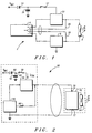
- FIG. 1 shows a known igniter system 2 comprising a processing unit 4 for generating the firing signal when an accident occurs and for performing diagnostics, and a hot wire bridge igniter element 6.
- a low side switch 8 couples a first terminal of the igniter element 6 to ground and a high side switch 10 couples a second terminal of the igniter element 6 to a battery voltage (Vbat) via a switch 12, which may be a mechanical crash sensor, and a diode 14.
- a reservoir capacitor 16, coupled to a node between the diode and switch 12, ensures that when an accident occurs and switch 12 and high side switch 10 are closed, sufficient power is provided to fire the igniter element 6 even when the battery has been disconnected.
- the high side switch 10 and low side switch 8 are opened and closed under the control of the processing unit 4.
- the igniter system 2 When an accident occurs, the igniter system 2 operates in a firing mode wherein switch 12 is closed, the processing unit 4 closes both the low 8 and high 10 side switches so that current from the battery flows through the igniter element 6, and heats the element until it fires and ignites adjacent pyrotechnic material (not shown).
- the hot wire bridge igniter element 6 has a resistance of 2 ohms and is fired when a current of 1.5 A flows therethrough for 2 ms.
- the igniter system 2 also operates in a diagnostic mode wherein a current of between 15 and 30 mA is passed through the igniter element 6 and the voltage signal across the igniter element 6 is provided to the processing unit 4 via diagnostic wires 18, 20.
- the processing unit uses the voltage signal to determine the resistance of the igniter element 6 and to determine whether the first and second terminals of the igniter element 6 are open circuit, short circuit to battery or ground.
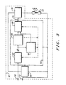
- an igniter system 50 in accordance with a preferred embodiment of the invention comprises a control circuit 52 for controlling the power supplied to an igniter element 54.
- the control circuit 52 has a first input 70 coupled to a first voltage supply, battery voltage (Vbat), via a high side switch 56, a switch 58 and a diode 60 and a second input 72 coupled to a reference voltage, preferably ground.
- a reservoir capacitor 62 is coupled to a node 64 between the switch 58, which may be a mechanical crash sensor, and the diode 60.
- the high side switch 56 is open and closed under the control of a processing unit 66 which supplies a signal to a control input of the high side switch 56.
- Processing unit 66 may be an airbag MCU.
- An encoded input signal is supplied under the control of the processing unit 66 via a load resistor 68 to the first input 70 of the control circuit 52.
- the igniter element 54 comprises a semiconductor igniter element such as a semiconductor igniter element.
- the control circuit 52 and the igniter element 54 can therefore be integrated onto one igniter device chip which significantly improves EMC performance.
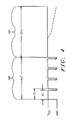
- FIG. 3 shows the control circuit 52 in accordance with the preferred embodiment in more detail.
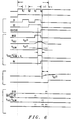
- the first input 70 of the control circuit 52 is coupled to receive the encoded input signal generated by the processing unit 66, such as the encoded input signal shown in FIG. 4, and the second input 72 is coupled to ground.
- the encoded input signal comprises a code portion 100 and a power portion 102.
- the code portion comprises at least two pulses having substantially the same frequency (1/T). The preferred number of pulses is four, which number allows the code portion to be verified in a reasonable time and with significantly less risk of parasitics corrupting the verification process. The following description will however be directed to a code portion 100 comprising four pulses but it is not intended that the invention be limited to a four pulse code portion. Preferably, the code portion has a duration of less than 6 ⁇ s.
- the power portion 102 comprises a signal having a constant voltage level Vcc or one which decays with time as shown by the dotted lines on FIG. 4. The power portion 102 does not supply enough power to fire the igniter element 54.
- the control circuit 52 comprises logic means 74 coupled to the first input 70 for determining whether the code portion of a received encoded input signal is valid and for providing an unlocking signal at an output 76 when the code portion is determined to be valid.
- the control circuit further comprises a switch 78 having an input coupled to the first input 70, a control input coupled to the output 76 of the logic means 74 and an output coupled to the igniter element 54.
- the switch 78 is enabled in response to receiving the unlocking signal at its control input and when enabled, supplies the power portion 102 of the received signal to the igniter element.
- the switch 78 may comprise a MOS transistor or a thyristor or any other type of switch.
- a power supply 80 supplies power to the logic means 74 and derives its energy from the received encoded input signal.
- the logic means 74 comprises a counter 82 which is clocked by the received encoded input signal for counting the number of pulses in the code portion 100 of the received encoded input signal.
- An output of the counter 82 is coupled both to a first logic circuit 84 and a second logic circuit 86.
- the first logic circuit 84 determines the number of pulses in the code portion 100 and provides a valid signal to an unlocking circuit 88 when the code portion 100 comprises only four pulses and a reset signal when the code portion 100 comprises any number of pulses other than four.
- the second logic circuit 86 determines whether the code portion 100 meets predefined conditions within a predetermined time window and if it does, a valid signal is provided to the unlocking circuit 88 but if it does not, a reset signal is generated.
- the unlocking circuit 88 on receipt of valid signals from both the first 84 and second 86 logic circuits, which indicates that the code portion is valid, then generates the unlocking signal. If either of the first 84 or second 86 logic circuits generate a reset signal, the counter 82 and unlocking circuit 88 are reset.
- FIG. 5 shows the logic means 74 and power supply 80 in accordance with the preferred embodiment in more detail.
- the power supply 80 comprises a Shottky diode 90 and a capacitor 92 and supplies a voltage supply signal Vsupply to each of the logic gates of the logic means 74.
- the counter 82 is clocked by the received encoded input signal so as to provide three output signals Q1, Q2, Q3.
- the first Q1 and second Q2 output signals are coupled to respective inputs of a first AND logic gate 94.
- the output signal (Q1.Q2) of first AND logic gate 94 is coupled to first 98 and second 104 delay circuits.
- Each of the first 98 and second 104 delay circuits comprise a resistor and capacitor whose values are chosen so that the time constant or first predetermined delay of the first delay circuit 98 is less than the second predetermined delay of the second delay circuit 104 (R1C1 ⁇ R2C2).
- the first delay circuit 98 provides a first delayed output signal Vfast to a first input of a second AND logic gate 96 and the second delay circuit 104 provides a second delayed output signal Vslow to a second inverted input of the second AND logic gate 96.
- the output signal Vslow .Vfast of the second AND logic gate 96 is coupled to a data input D of a latch, such as a D-type flip-flop 106.
- the first 98 and second 104 delay circuits determine the time window in which the code portion 100 must meet predefined conditions in order for the code portion 100 to be determined to be valid.
- the flip-flop 106 is clocked by the third output signal D3 provided by the counter 82.
- the signal Qd at the output of the flip-flop 106 is coupled to a Schmitt trigger 108 via a third RC delay circuit 110.
- the signal Sfire at the output of the Schmitt trigger 108 provides the unlocking signal which is coupled to the control input of the switch 78.
- the unlocking circuit 88 comprises the flip-flop 106, Schmitt trigger 108, and the third delay circuit 110.
- the first Q1 and third Q3 output signals provided by the counter 82 are also coupled to respective inputs of a third AND logic gate 112.
- the output signal Q1.Q3 of the third AND logic gate 112 is coupled to a first input of an OR logic gate 114.
- the first and second delayed output signals Vfast and Vslow of the first 98 and second 104 delay circuits are coupled to respective inputs of a fourth AND logic gate 116.
- the output signal Vslow.Vfast of the fourth AND logic gate 116 is coupled to a second input of the OR logic gate 114.
- the third output signal Q3 of the counter 82, the inverse Vfast of the first delayed output signal of the first delay circuit 98 and the inverse Qd of the output signal of the flip-flop 106 are coupled to respective inputs of a fifth AND logic gate 118.
- Qd of the fifth AND logic gate 118 is coupled to a third input of the OR logic gate 114.
- the output signal of the OR logic gate 114 provides the reset signal which is coupled to the reset input of the counter 82 and the reset input of the flip-flop 106.
- the first logic circuit 84 comprises the third AND logic gate 112 and the third output signal Q3 which clocks the flip-flop 106 and the second logic circuit 86 comprises the first 94, second 96, fourth 116 and fifth 118 AND logic gates, and the first 98 and second 104 delay circuits.
- control circuit 52 in accordance with the present invention to verify the validity of the code portion 100 of a received encoded input signal and to unlock the igniter element 54 will now be described with reference also to FIG. 6 which shows the timing diagrams for the signals generated by the different components of control circuit 52.
- the processing unit 66 In order to unlock the igniter element 54, the processing unit 66 generates the encoded input signal which it supplies to the first input 70 of the control circuit 52 via load resistor 68.
- the first rising edge of the encoded input signal is used to charge the capacitor 92 through the Shottky diode 90.
- No limitation resistor is used to ensure that the capacitor 92 is correctly charged after the first pulse in a very short time.
- the energy which is stored in capacitor 92 is used as power supply Vsupply for the logic means 74.
- the four consecutive falling edges of the code portion of the encoded input signal are used as the clock signal for the counter 82 which generates the three output signals Q1, Q2, Q3 as shown in the timing diagrams of FIG. 6.
- the output signal Q1.Q2 of the first AND logic gate 94 charges the capacitances C1, C2 of respective first 98 and second 104 delay circuits so as to provide the first and second delayed output signals Vfast and Vslow respectively.
- the signal at the first input of the second AND logic gate 96 represents a logic '1' and when the second delayed output signal Vslow is below a predetermined value Vcc/2, the inverted signal at the second inverted input of the second AND logic gate 96 also represents a logic '1'.
- the output signal Vslow .Vfast of the second AND logic gate 96 can be used to set a predetermined time window for the code portion 100.
- the output signal Vslow .Vfast is a logic '1' when the counter's third output signal Q3 changes from logic '0' to a logic '1'. This allows the output signal Qd of the flip-flop 106 to switch from logic '0' to logic '1'.
- the signal Qd is therefore generated as the counter 82 counts the falling edge of the fourth pulse as long as the timing conditions dictated by the first 98 and second 104 delay circuits are met.
- a delay 120 is introduced by the third delay circuit 110 and Schmitt trigger 108 which delay Td is shown in FIG.
- the unlocking signal Sfire having a logic '1' is generated once the delay Td has expired and no additional pulse has been counted which indicates that the received code portion is valid.
- the unlocking signal enables the switch 78 which unlocks the igniter system 50.
- the logic means 74 works normally up to the R3.C3 time constant.
- An advantage of the present invention is that the when the code portion is determined to be invalid, the logic means 74 is reset asynchronously so that all the components of the logic means 74 are reset and in the right condition should the igniter element 54 need to be fired.
- the control circuit 52 in accordance with the present invention thus provides enhanced protection against inadvertent firing of the igniter element 54, having three levels of protection corresponding to the three conditions.
- the present invention ensure that the code portion 100 of the received encoded input signal is verified by the logic means 74 to determine whether the code portion is valid.
- the logic means 74 determines that the code portion 100 satisfies certain predefined conditions within a predetermined time window, the code portion is determined to be valid and an unlocking signal is generated which enables the switch 78.
- the power portion of the received encoded input signal is then supplied to the igniter element 54.
- the switch 78 is only enabled when the code portion is determined to be valid. This means that power can only be supplied to the igniter element 54 when the logic means 74 verifies that the code portion 100 is valid.
- the igniter system is locked.
- the igniter system 50 is required to be unlocked during a firing mode when an accident occurs and the igniter element 54 is to be fired and during a diagnostic mode when the processing unit 66 carries out diagnostics on the igniter element 54 to determine that the igniter element is functioning correctly.
- the processing unit 66 provides the encoded input signal comprising a code portion 100 and a power portion 102 to the first input 70 of the control circuit 52.
- the firing mode is entered when an accident occurs.
- the processing unit 66 supplies the encoded input signal comprising a four pulse code portion 100 and the power portion 102 to the control circuit 52. Once the control circuit 52 has determined that the code portion 100 is valid, the switch 78 is enabled and the power portion 102 of the encoded input signal is provided to the igniter element 54. The power portion 102 does not have sufficient energy to fire the igniter element 54.
- the processing unit 66 provides a control signal to the control input of the high side switch 56 and the switch 58 is closed so that power from the battery voltage Vbat or reservoir capacitor 62 is supplied to the igniter element 54 which fires the igniter element 54.
- control circuit 52 and igniter element 54 are not supplied with any current. The stand-by consumption is therefore zero.
- the diagnostic mode is entered under the control of the processing unit 66.
- the high side switch 56 and switch 58 remain open so that no power is supplied by the batter voltage Vbat or reservoir capacitor 62.
- the processing unit 66 supplies the encoded input signal comprising a four pulse code portion 100 and the power portion 102 to the control circuit 52.
- the switch 78 is enabled and the power portion 102 of the encoded input signal is provided to the igniter element 54.
- the power portion 102 comprises a low current signal to verify the integrity of the logic means 74 itself as well as the integrity of the igniter element 54 (open, short circuit and resistance of igniter element).
- the current signal must be low enough to limit the heat generation of the igniter element 54 which could alter the chemical nature of the pyrotechnic material surrounding the igniter element. Since the logic means 74 only allows the igniter element 54 to be fired on receipt of a valid code, the logic means 74 provides protection against ESD and RF perturbations. This means that the resistance of the igniter element 54 can be increased with the result that the voltage signals to be measured in the diagnostic mode have a higher level and can be measured more accurately. Thus, the present invention allows for more accurate diagnostics than the prior art arrangements described above.
- the present invention provides a robust, simple control circuit for controlling the power delivered to the igniter element so that only a specific code generated by the processing unit will unlock the igniter system and allow the igniter element to be fired or for diagnostics to be carried out.
- the enhanced three-level protection provided by the control circuit ensures that bad codes can be detected and the control circuit reset for the next received code.
- the simple technique employed by the control circuit in accordance with the invention to determine the validity of a code portion of an encoded input signal means that only simple logic is needed for its implementation which reduces the die size of such a circuit.
- control circuit in accordance with the present invention is powered by the encoded input signal supplied by the processing unit, the control circuit and igniter element can be integrated on the same chip and the integrated chip only requires two connection wires. Such a solution is therefore compatible with existing systems.
- control circuit and igniter element may be implemented using CMOS technology which improves noise immunity and tolerance due to power supply variations.
- a full wave rectifier circuit may be coupled across the first 70 and second 72 inputs of the control circuit 52. This optional feature ensures that the control circuit 52 is symmetrical; it does not matter which way round the first 70 and second 72 inputs are connected.
Landscapes
- Engineering & Computer Science (AREA)
- Mechanical Engineering (AREA)
- General Engineering & Computer Science (AREA)
- Air Bags (AREA)
Description
Claims (10)
- A control circuit (52) for controlling power supplied to an igniter element (54), the control circuit comprising:a first input (70) for receiving an encoded input signal generated in response to the initiation of a firing mode and a diagnostic mode, the encoded input signal comprising a code portion (100) and a power portion (102), the code portion comprising n pulses having substantially a predetermined frequency, where n is at least two;logic means (74) for determining whether the code portion of the received encoded input signal is valid, the code portion being determined valid when the code portion meets predefined conditions within a predetermined time window and for providing an unlocking signal at an output (76) when the code portion is determined to be valid; anda switch (78) having a control input coupled to the output (76) of the logic means, an input coupled to the first input (70) of the control circuit, and an output for coupling to the igniter element (54), wherein the switch (78) is enabled on receipt of the unlocking signal such that in the firing mode power, including the power portion of the received encoded input signal, at the first input (70) of the control circuit is supplied to the output of the switch (78) for firing the igniter element (54) and in the diagnostic mode, the power portion of the received encoded input signal is supplied to the output of the switch (78) for energising the igniter element (54).
- A control circuit according to claim 1 further comprising a power supply (80) coupled between the first input (70) of the control circuit and a second input (72) of the control circuit which second input is coupled to a reference voltage, the power supply deriving energy from the encoded input signal so as to supply power at an output to the logic means.
- A control circuit according to claim 2 wherein the power supply comprises a diode (90) coupled in series with a capacitor (92) between the first (70) and second (72) inputs of the control circuit (52) the output of the power supply being coupled to a node between the capacitor (92) and diode (90).
- A control circuit according to claim 2 or 3 further comprising a full wave rectifier circuit coupled across the first (70) and second (72) inputs of the control circuit.
- A control circuit according to claim 1, 2, 3 or 4 wherein the logic means (74) comprises:a counter (82) having a clock input coupled to the first input (70) of the control circuit so as to receive the encoded input signal for counting each pulse in the code portion of the encoded input signal;a first logic circuit (84) coupled to the counter (82) for determining the number of pulses in the code portion and for providing a valid signal when the code portion is determined to comprise n pulses and a reset signal when the code portion is determined to comprise any other number of pulses;a second logic circuit (86) coupled to the counter (82) for determining whether the code portion meets predefined conditions within the predetermined time window, the predefined conditions including a condition that the predetermined frequency of the code portion is within a predetermined range, and for providing a valid signal when the predefined conditions are met within the predetermined time window and a reset signal when the predefined conditions are not met within the predetermined time window; andan unlocking circuit (88) coupled to receive the valid signals and reset signals from the first (84) and second (86) logic circuits, for generating the unlocking signal on receipt of the valid signals from both the first and second logic circuits and for being reset in response to receiving a reset signal from one of the first and second logic circuits.
- A control circuit according to claim 5 wherein n is equal to four such that the code portion comprises four pulses.
- A control circuit according to claim 6 wherein the counter is clocked by the code portion of the encoded input signal to provide first, second and third output signals,
wherein the first logic circuit (84) comprises a third AND logic gate (112) having first and second inputs coupled to receive the first and third output signals provided by the counter and an output for providing the reset signal,
wherein the second logic circuit (86) comprises:wherein the unlocking circuit (88) comprises:a first AND logic gate (94) having first and second inputs coupled to receive respective first and second output signals provided by the counter and an output;first delay circuit (98) coupled to the output of the first AND logic gate (94) for delaying the signal at the output of the first AND logic gate (94) by a first predetermined delay and for providing a first delayed output signal;second delay circuit (104) coupled to the output of the first AND logic gate (94) for delaying the signal at the output of the first AND logic gate by a second predetermined delay and for providing a second delayed output signal, the first and second predetermined delays being different so as to define the predetermined time window;a second AND logic gate (96) having a first input coupled to receive the first delayed output signal, a second inverted input coupled to receive the second delayed output signal and an output;a fourth AND logic gate (116) having first and second inputs coupled to receive respective first and second delayed output signals and an output for providing the reset signal; anda fifth AND logic gate (118) having a first inverted input coupled to receive the first delayed output signal, a second input coupled to receive the third output signal provided by the counter, a third input and an output for providing the reset signal, anda latch (106) having a clock input coupled to receive the third signal provided by the counter, a data input coupled to the output of the second AND logic gate (96), a reset input coupled to receive the reset signals, and an output coupled to the third input of the fifth AND logic gate (118);third delay circuit (110) coupled to the output of the latch for delaying the signal at the output of the latch so as to provide a delayed output signal; anda Schmitt trigger (108) coupled to the third delay circuit (110) for generating the unlocking signal when the delayed output signal reaches a predetermined level, the latch (106) being reset on receipt of one of the reset signals such that the unlocking signal is not generated. - A control circuit according to claim 7 wherein the logic means (74) further comprises an OR logic gate (114) coupled to the outputs of the third (112), fourth (116) and fifth (118) AND logic gates, the OR logic gate (114) having an output for providing a reset signal to the reset input of the latch (106) and a reset input of the counter (82).
- An igniter device comprising a semiconductor igniter element (54) and a control circuit (52) according to any preceding claim, wherein the semiconductor igniter element and the control circuit are integrated on the same chip.
- An igniter system comprising:a control circuit (52) according to any preceding claim;an igniter element (54) coupled to the output of the switch (78) of the control circuit such that when the control circuit switch (78) is enabled power is supplied to the igniter element;a power switch (56) coupled to the first input (70) of the control circuit (52) and a first voltage supply, the power switch when enabled providing a power signal to the first input of the control circuit;a processing unit (66) for generating the encoded input signal generated in response to the initiation of a firing mode and a diagnostic mode and for providing the encoded input signal to the first input (70) of the control circuit (52), for providing a control signal to the power switch (56) to enable the power switch in response to the initiation of the firing mode, and for monitoring a voltage signal across the igniter element in the diagnostic mode, wherein in the firing mode the power signal at the first input (70) of the control circuit (52) is supplied with the power portion (102) of the encoded input signal to the igniter element (54) when the control circuit (52) enables the control circuit switch (78) to fire the igniter element (54), and wherein in the diagnostic mode the processing unit (66) does not enable the power switch (56) wherein only the power portion (102) of the encoded input signal is provided to the igniter element (54) when the control circuit enables the control circuit switch (78).
Applications Claiming Priority (3)
| Application Number | Priority Date | Filing Date | Title |
|---|---|---|---|
| FR9601675A FR2744862B1 (en) | 1996-02-12 | 1996-02-12 | CIRCUIT FOR CONTROLLING THE ELECTRICAL SUPPLY OF AN IGNITOR ELEMENT |
| FR9601675 | 1996-02-12 | ||
| PCT/EP1997/000478 WO1997029932A1 (en) | 1996-02-12 | 1997-02-03 | Control circuit for controlling power supplied to an igniter element and igniter system |
Publications (2)
| Publication Number | Publication Date |
|---|---|
| EP0819071A1 EP0819071A1 (en) | 1998-01-21 |
| EP0819071B1 true EP0819071B1 (en) | 2001-01-31 |
Family
ID=9489075
Family Applications (1)
| Application Number | Title | Priority Date | Filing Date |
|---|---|---|---|
| EP97902306A Expired - Lifetime EP0819071B1 (en) | 1996-02-12 | 1997-02-03 | Control circuit for controlling power supplied to an igniter element and igniter system |
Country Status (8)
| Country | Link |
|---|---|
| US (1) | US5957988A (en) |
| EP (1) | EP0819071B1 (en) |
| JP (1) | JPH11504704A (en) |
| KR (1) | KR100458343B1 (en) |
| CN (1) | CN1085160C (en) |
| DE (1) | DE69704006T2 (en) |
| FR (1) | FR2744862B1 (en) |
| WO (1) | WO1997029932A1 (en) |
Families Citing this family (24)
| Publication number | Priority date | Publication date | Assignee | Title |
|---|---|---|---|---|
| JPH11180248A (en) * | 1997-12-22 | 1999-07-06 | Takata Kk | Ignition device for air bag |
| DE19822780A1 (en) * | 1998-05-20 | 1999-12-09 | Siemens Ag | Method and device for checking an electrical circuit, in particular an ignition circuit of a motor vehicle occupant protection system |
| DE19836197C2 (en) * | 1998-08-10 | 2001-06-28 | Breed Automotive Tech | Device for preparing an electric ignition device of a tensioner drive for tightening a seat belt |
| US6166452A (en) * | 1999-01-20 | 2000-12-26 | Breed Automotive Technology, Inc. | Igniter |
| EP1237761B1 (en) | 1999-12-16 | 2004-09-01 | Siemens Aktiengesellschaft | Method for testing an ignition device and a corresponding ignition device |
| US6275756B1 (en) * | 2000-06-21 | 2001-08-14 | Breed Automotive Technology, Inc. | Smart ignitor control system |
| DE10123215A1 (en) * | 2001-05-12 | 2002-12-12 | Bosch Gmbh Robert | Method for activating an occupant protection application in a motor vehicle |
| US6490976B1 (en) | 2001-08-22 | 2002-12-10 | Breed Automotive Technology, Inc. | Smart igniter communications repeater |
| US7155353B2 (en) * | 2002-04-25 | 2006-12-26 | Daicel Chemical Industries, Ltd. | Method for determining charging capacitance of capacitor |
| US6732656B1 (en) | 2002-09-16 | 2004-05-11 | The United States Of America As Represented By The Secretary Of The Air Force | High voltage tolerant explosive initiation |
| DE10252990B3 (en) * | 2002-11-14 | 2004-04-15 | Siemens Ag | Control unit for a motor vehicle occupant safety system, especially an airbag system, has additional AND gates in addition to dual controlling computers to ensure reliable detection and resetting of a faulty computer unit |
| DE10259546A1 (en) * | 2002-12-19 | 2004-07-01 | Robert Bosch Gmbh | Device for wireless transmission of a trigger signal |
| US6799999B2 (en) * | 2003-02-07 | 2004-10-05 | Fci Americas Technology, Inc. | Filtered electrical connector |
| US6997750B2 (en) | 2003-07-23 | 2006-02-14 | Fci Americas Technology, Inc. | Electrical connector contact |
| US7857794B2 (en) * | 2004-06-14 | 2010-12-28 | Alcon, Inc. | Handpiece tip |
| JP5175782B2 (en) * | 2009-03-24 | 2013-04-03 | トヨタ自動車株式会社 | Remote control system and portable device |
| DE102011087077A1 (en) * | 2011-11-25 | 2013-05-29 | Robert Bosch Gmbh | Method and arrangement for controlling at least one triggering element for a personal protection device |
| US9283912B2 (en) * | 2013-06-27 | 2016-03-15 | Zodiac Cabin Controls Gmbh | Airbag control unit |
| KR20150062760A (en) * | 2013-11-29 | 2015-06-08 | 에스케이하이닉스 주식회사 | Flip-Flop Circuit and Semiconductor Apparatus Using the Same |
| DE102014207302A1 (en) * | 2014-04-16 | 2015-10-22 | Robert Bosch Gmbh | Method and device for switching off at least one ignition output stage for a squib of a pyrotechnic protective agent for a vehicle |
| DE102019204033B3 (en) * | 2019-03-25 | 2020-07-23 | Volkswagen Aktiengesellschaft | Electrical fuse, method of operating an electrical fuse and electrical traction network |
| DE102020124056A1 (en) * | 2020-09-15 | 2022-03-17 | Bayerische Motoren Werke Aktiengesellschaft | Method and control unit for protection against unauthorized installation of a pyrotechnic component |
| EP4484226A1 (en) * | 2023-06-30 | 2025-01-01 | NXP USA, Inc. | Device, system and method |
| CN120065798B (en) * | 2024-09-30 | 2026-04-03 | 天水七四九电子有限公司 | An ignition circuit system based on digital structure |
Family Cites Families (10)
| Publication number | Priority date | Publication date | Assignee | Title |
|---|---|---|---|---|
| DE2158930A1 (en) * | 1971-11-27 | 1973-06-07 | Volkswagenwerk Ag | AIR-BAG-SYSTEM |
| FR2467740A1 (en) * | 1979-10-23 | 1981-04-30 | Renault | SYSTEM FOR DETECTING COLLISIONS AND CONTROLLING A SAFETY DEVICE |
| US4359715A (en) * | 1980-12-22 | 1982-11-16 | Ford Motor Company | Coded failure indicator for an air bag system |
| US4950914A (en) * | 1987-03-30 | 1990-08-21 | Honda Giken Kogyo Kabushiki Kaisha | Collision detection system for a vehicle |
| JP2578368B2 (en) * | 1988-04-15 | 1997-02-05 | ダイムラー―ベンツ・アクチエンゲゼルシヤフト | Detector and energy supply device for circuit including load to be monitored |
| US5422965A (en) * | 1992-02-18 | 1995-06-06 | Hitachi, Ltd. | Air bag operation device |
| JP2661863B2 (en) * | 1993-10-29 | 1997-10-08 | 富士通テン株式会社 | Squib line diagnostic device for airbag system of vehicle |
| JPH07228215A (en) * | 1994-02-17 | 1995-08-29 | Mitsubishi Electric Corp | Control circuit for vehicle safety device |
| US5749059A (en) * | 1995-09-14 | 1998-05-05 | Trw Technar Inc. | Apparatus and method for controlling an actuatable restraint device |
| GB2310303B (en) * | 1996-02-13 | 1999-07-28 | Autoliv Dev | Improvements in or relating to a crash detector arrangement |
-
1996
- 1996-02-12 FR FR9601675A patent/FR2744862B1/en not_active Expired - Fee Related
-
1997
- 1997-02-03 EP EP97902306A patent/EP0819071B1/en not_active Expired - Lifetime
- 1997-02-03 KR KR1019970707295A patent/KR100458343B1/en not_active Expired - Fee Related
- 1997-02-03 DE DE69704006T patent/DE69704006T2/en not_active Expired - Fee Related
- 1997-02-03 WO PCT/EP1997/000478 patent/WO1997029932A1/en not_active Ceased
- 1997-02-03 CN CN97190190A patent/CN1085160C/en not_active Expired - Fee Related
- 1997-02-03 JP JP9528938A patent/JPH11504704A/en not_active Ceased
- 1997-02-03 US US08/930,294 patent/US5957988A/en not_active Expired - Fee Related
Also Published As
| Publication number | Publication date |
|---|---|
| KR19980703894A (en) | 1998-12-05 |
| KR100458343B1 (en) | 2005-06-01 |
| US5957988A (en) | 1999-09-28 |
| CN1085160C (en) | 2002-05-22 |
| CN1181732A (en) | 1998-05-13 |
| FR2744862A1 (en) | 1997-08-14 |
| WO1997029932A1 (en) | 1997-08-21 |
| FR2744862B1 (en) | 1998-04-30 |
| DE69704006D1 (en) | 2001-03-08 |
| JPH11504704A (en) | 1999-04-27 |
| EP0819071A1 (en) | 1998-01-21 |
| DE69704006T2 (en) | 2001-07-19 |
Similar Documents
| Publication | Publication Date | Title |
|---|---|---|
| US5957988A (en) | Control circuit for controlling power supplied to an igniter element and igniter system | |
| US4864202A (en) | Method and apparatus for monitoring the operation of a computer-controlled operating element, particularly triggered safety apparatus for an automotive vehicle | |
| RU2077699C1 (en) | Device to initiate electric loads, method of initiation of electric loads after expiry of time delays set in advance and remote electric device to delay initiation of electric load | |
| US6597181B2 (en) | High and low side driver tests for airbag module | |
| US5446442A (en) | Circuit arrangement for triggering a vehicle passenger protection system | |
| US5146104A (en) | Electronic device for triggering a safety device | |
| US5194755A (en) | Airbag triggering system | |
| US4243971A (en) | Test circuit for automotive passenger restraint systems | |
| KR950003268B1 (en) | Ignition Circuit of Air Bag System | |
| CN103135030A (en) | System and method for testing a power supply controller | |
| KR100392920B1 (en) | Method for checking the capacitance of memory-capacitor provided in a passenger-protecting-system and testing apparatus | |
| US20040020392A1 (en) | Electronic switching system for a detonation device, method of operation and explosive device including same | |
| US7142407B2 (en) | Squib driver for airbag application | |
| KR20160008588A (en) | Method and apparatus for identifying a polarity of a freewheeling diode, actuator circuit and safety apparatus for a vehicel | |
| US4438424A (en) | Electric apparatus for a vehicle safety device | |
| EP0558513B1 (en) | Test circuit for detection of malfunctions in an electric triggering device in a vehicle occupant protection device | |
| US5549325A (en) | Activating device in a passenger protection apparatus | |
| US6028431A (en) | On-board wiring fault detection device | |
| US6507053B1 (en) | Highly reliable OTP device | |
| US6864599B1 (en) | System and method for testing an ignition device | |
| EP0547693B1 (en) | Circuit arrangement comprising an end-of-life detector | |
| CN120474525A (en) | Delay system, controller power supply system, controller power supply method and vehicle | |
| JP3319179B2 (en) | Explosive element ignition device | |
| White et al. | Inflatable restraint sensing and diagnostic strategy | |
| JP3927906B2 (en) | Method for enabling at least two separately ignitable ignition stages in an occupant protection system to be ignitable, and an electrical enable circuit for the occupant protection system |
Legal Events
| Date | Code | Title | Description |
|---|---|---|---|
| PUAI | Public reference made under article 153(3) epc to a published international application that has entered the european phase |
Free format text: ORIGINAL CODE: 0009012 |
|
| AK | Designated contracting states |
Kind code of ref document: A1 Designated state(s): DE GB IT |
|
| 17P | Request for examination filed |
Effective date: 19980223 |
|
| 17Q | First examination report despatched |
Effective date: 19990726 |
|
| GRAG | Despatch of communication of intention to grant |
Free format text: ORIGINAL CODE: EPIDOS AGRA |
|
| RIC1 | Information provided on ipc code assigned before grant |
Free format text: 7F 42C 11/00 A, 7B 60R 21/00 B |
|
| GRAG | Despatch of communication of intention to grant |
Free format text: ORIGINAL CODE: EPIDOS AGRA |
|
| GRAH | Despatch of communication of intention to grant a patent |
Free format text: ORIGINAL CODE: EPIDOS IGRA |
|
| GRAH | Despatch of communication of intention to grant a patent |
Free format text: ORIGINAL CODE: EPIDOS IGRA |
|
| GRAA | (expected) grant |
Free format text: ORIGINAL CODE: 0009210 |
|
| AK | Designated contracting states |
Kind code of ref document: B1 Designated state(s): DE GB IT |
|
| PG25 | Lapsed in a contracting state [announced via postgrant information from national office to epo] |
Ref country code: IT Free format text: LAPSE BECAUSE OF FAILURE TO SUBMIT A TRANSLATION OF THE DESCRIPTION OR TO PAY THE FEE WITHIN THE PRESCRIBED TIME-LIMIT;WARNING: LAPSES OF ITALIAN PATENTS WITH EFFECTIVE DATE BEFORE 2007 MAY HAVE OCCURRED AT ANY TIME BEFORE 2007. THE CORRECT EFFECTIVE DATE MAY BE DIFFERENT FROM THE ONE RECORDED. Effective date: 20010131 |
|
| REF | Corresponds to: |
Ref document number: 69704006 Country of ref document: DE Date of ref document: 20010308 |
|
| EN | Fr: translation not filed | ||
| PLBE | No opposition filed within time limit |
Free format text: ORIGINAL CODE: 0009261 |
|
| STAA | Information on the status of an ep patent application or granted ep patent |
Free format text: STATUS: NO OPPOSITION FILED WITHIN TIME LIMIT |
|
| REG | Reference to a national code |
Ref country code: GB Ref legal event code: IF02 |
|
| 26N | No opposition filed | ||
| PGFP | Annual fee paid to national office [announced via postgrant information from national office to epo] |
Ref country code: GB Payment date: 20040107 Year of fee payment: 8 |
|
| PGFP | Annual fee paid to national office [announced via postgrant information from national office to epo] |
Ref country code: DE Payment date: 20040227 Year of fee payment: 8 |
|
| PG25 | Lapsed in a contracting state [announced via postgrant information from national office to epo] |
Ref country code: GB Free format text: LAPSE BECAUSE OF NON-PAYMENT OF DUE FEES Effective date: 20050203 |
|
| PG25 | Lapsed in a contracting state [announced via postgrant information from national office to epo] |
Ref country code: DE Free format text: LAPSE BECAUSE OF NON-PAYMENT OF DUE FEES Effective date: 20050901 |
|
| GBPC | Gb: european patent ceased through non-payment of renewal fee |
Effective date: 20050203 |