EP0818034B1 - Black level setting - Google Patents
Black level setting Download PDFInfo
- Publication number
- EP0818034B1 EP0818034B1 EP97900023A EP97900023A EP0818034B1 EP 0818034 B1 EP0818034 B1 EP 0818034B1 EP 97900023 A EP97900023 A EP 97900023A EP 97900023 A EP97900023 A EP 97900023A EP 0818034 B1 EP0818034 B1 EP 0818034B1
- Authority
- EP
- European Patent Office
- Prior art keywords
- value
- control
- black level
- predetermined ratio
- iref1
- Prior art date
- Legal status (The legal status is an assumption and is not a legal conclusion. Google has not performed a legal analysis and makes no representation as to the accuracy of the status listed.)
- Expired - Lifetime
Links
- 230000004044 response Effects 0.000 claims abstract description 8
- 238000000034 method Methods 0.000 claims abstract description 5
- 230000001419 dependent effect Effects 0.000 description 3
- 230000006870 function Effects 0.000 description 3
- 238000005259 measurement Methods 0.000 description 3
- 238000012937 correction Methods 0.000 description 2
- 238000012546 transfer Methods 0.000 description 2
- 239000003990 capacitor Substances 0.000 description 1
- 238000009125 cardiac resynchronization therapy Methods 0.000 description 1
- 238000013461 design Methods 0.000 description 1
- 230000006641 stabilisation Effects 0.000 description 1
- 238000011105 stabilization Methods 0.000 description 1
Images
Classifications
-
- G—PHYSICS
- G09—EDUCATION; CRYPTOGRAPHY; DISPLAY; ADVERTISING; SEALS
- G09G—ARRANGEMENTS OR CIRCUITS FOR CONTROL OF INDICATING DEVICES USING STATIC MEANS TO PRESENT VARIABLE INFORMATION
- G09G3/00—Control arrangements or circuits, of interest only in connection with visual indicators other than cathode-ray tubes
- G09G3/20—Control arrangements or circuits, of interest only in connection with visual indicators other than cathode-ray tubes for presentation of an assembly of a number of characters, e.g. a page, by composing the assembly by combination of individual elements arranged in a matrix no fixed position being assigned to or needed to be assigned to the individual characters or partial characters
-
- H—ELECTRICITY
- H04—ELECTRIC COMMUNICATION TECHNIQUE
- H04N—PICTORIAL COMMUNICATION, e.g. TELEVISION
- H04N5/00—Details of television systems
- H04N5/44—Receiver circuitry for the reception of television signals according to analogue transmission standards
- H04N5/57—Control of contrast or brightness
- H04N5/59—Control of contrast or brightness in dependence upon beam current of cathode ray tube
-
- H—ELECTRICITY
- H04—ELECTRIC COMMUNICATION TECHNIQUE
- H04N—PICTORIAL COMMUNICATION, e.g. TELEVISION
- H04N5/00—Details of television systems
- H04N5/14—Picture signal circuitry for video frequency region
- H04N5/16—Circuitry for reinsertion of DC and slowly varying components of signal; Circuitry for preservation of black or white level
-
- H—ELECTRICITY
- H04—ELECTRIC COMMUNICATION TECHNIQUE
- H04N—PICTORIAL COMMUNICATION, e.g. TELEVISION
- H04N9/00—Details of colour television systems
- H04N9/64—Circuits for processing colour signals
- H04N9/645—Beam current control means
-
- H—ELECTRICITY
- H04—ELECTRIC COMMUNICATION TECHNIQUE
- H04N—PICTORIAL COMMUNICATION, e.g. TELEVISION
- H04N9/00—Details of colour television systems
- H04N9/64—Circuits for processing colour signals
- H04N9/72—Circuits for processing colour signals for reinsertion of DC and slowly varying components of colour signals
Definitions
- the invention relates to a method and a circuit for black level setting, and to a display apparatus including a black level setting circuit.
- US-A-5,278,476 discloses a display apparatus including a black level setting circuit with a control circuit adapted to successively apply at least two control voltages in a predetermined ratio to the cathode of the display device.
- the black level setting circuit includes a correction circuit for supplying a correction value dependent on the ratio between the currents generated in the relevant cathode in response to the at least two control voltages.
- a multiplier circuit provides a gain control to ensure that an arbitrary video voltage applied to the input yields the same cathode current for all three electron guns (cathodes), provided that the factors K and ⁇ are equal for all three cathodes.
- a first aspect of the invention provides a black level and gain control setting device as defined in claim 1.
- a second aspect of the invention provides a method of black level and gain control setting as defined in claim 6.
- a third aspect of the invention provides a display apparatus as defined in claim 7. Advantageous embodiments are defined in the dependent claims.
- a method of black level and gain control setting which comprises the steps of applying at least two mutually differing control values in a first predetermined ratio, and controlling the black level and gain in response to the at least two mutually differing control values, is characterized in that at least two mutually differing reference values in a second predetermined ratio and corresponding to the at least two mutually differing control values are applied to the controlling step, where a predetermined relationship exists between the first predetermined ratio and the second predetermined ratio, a first error value depending on a first control value and a first reference value is integrated to obtain a black level setting value, and a second error value depending on a second control value and a second reference value is integrated to obtain a gain setting value.
- the magnitudes of the cathode currents obtained in response to the control values are compared to the respective reference values to obtain error values. In a control loop, these error values are controlled to zero. Consequently, the magnitude of the cathode current no longer depends on the gain of a cathode drive circuit, the cut-off voltage and the factor K in the above-mentioned cathode current formula, but is exclusively determined by the magnitudes of the control values and reference values.
- US-A-4,370,674 discloses a stabilization network for a cathode ray tube which compensates for variable emission characteristics of a cathode in a television receiver's cathode ray tube.
- a variable gain video amplifier applies a black level DC voltage to the cathode.
- the resulting cathode current is sensed and compared to a low level reference current. If the cathode current does not equal the reference current, a control signal is applied to the amplifier.
- the amplifier responds to the control signal by changing its DC output voltage until the cathode current is equal to the reference current.
- the amplifier also responds to the control signal by altering its gain so that, when a video signal is received, the cathode develops peak white currents of a given value in response to peak white portions of the video signal. For example, a peak white reference current may be compared to cathode current in response to a simulated peak white output from the amplifier.
- an input video signal Vin is applied to a switch 42, whose output is connected to a cathode 9 of a display device D thru a gain control circuit (e.g. a multiplier) 35, a level control circuit (e.g. an adder) 3, a buffer circuit 5, and a video output stage 7.
- a measuring circuit 15 subtracts a reference signal received from a switch 47, from a signal related to the output current Ik supplied to the cathode 9 and received from the video output stage 7.
- An error current Ie from the measuring circuit 15 is applied to integrators (e.g. capacitors) 43 and 44 thru switches 46 and 45, respectively.
- the control circuits 35 and 3 are controlled by output signals of integrators 44 and 43, respectively, which function as memory elements. In a non-calibration state of the display apparatus, the switches 42, 45, 46 and 47 are in the positions shown.
- Calibration occurs in two phases.
- a first phase of the calibration state which occurs during a few measuring lines in a first field F1
- a first control voltage Vd1 is supplied to the circuit by the switch 42
- a first reference current Iref1 is applied to the measuring circuit 15 by the switch 47.
- switch 46 is closed.
- the cathode current Ik will have become equal to Irefl, so that the error current Ie is zero.
- a second control voltage Vd2 is supplied to the circuit by the switch 42, and a second reference current Iref2 is applied to the measuring circuit 15 by the switch 47.
- ⁇ 2.25, only a small error is made.
- the ratio to be selected between Vd1 and Iref1 (or between Vd2 and Iref2) depends on the desired gain of the transfer function.
- the absolute values of Vd1,2 and Iref1,2 do not influence the black level or the gain.
- a compromise has been sought between interference-susceptibility (which determines the minimum values of Vd1,2 and Iref1,2) and visibility of the measurement lines (which determine the maximum values of Vd1,2 and Irefl,2).
- an arrangement 48, 49 is present in addition to the elements of Fig. 1 , to compensate for leakage currents and for line frequency interference currents to the cathode connections.
- the switches 42 apply blanking voltages Vbl so that no current is applied to the cathodes.
- the switch 47 is in the position shown.
- the switch 48 is closed, so that the error current Ie is integrated by integrator 49 to set a compensation current Ic which compensates for all leakage and interference currents. After opening switch 48, the integrator 49 maintains the compensation current Ic.
- the measuring circuit 15 subtracts the compensation current Ic from the difference between the cathode current Ik and the reference current Iref1,2.
- Fig. 3 illustrates a complete calibration cycle.
- the blanking voltage Vbl is offered to all three cathodes 9.
- Var indicates the voltage applied to the red channel of the circuit
- Vag indicates the voltage applied to the green channel
- Vab indicates the voltage applied to the blue channel.
- the total leakage / interference current is measured and compensated for by closing switch 48 during this image line (see line SW48 in Fig. 3 ).
- the red channel is calibrated: its switch 46 is closed (see line SW46R in Fig. 3 ), and the control voltage Vd1 is supplied by its switch 42.
- the blanking voltage Vbl is supplied by their respective switches 42 so that the green and blue cathode currents do not influence calibration in the red channel.
- the green channel is calibrated: its switch 46 is closed (see line SW46G in Fig. 3 ).
- the blue channel is calibrated: its switch 46 is closed (see line SW46B in Fig. 3 ).
- the second phase which is carried out during a subsequent field F2, resembles the first phase to a large extent. Instead of switches 46R, 46G and 46B, switches 45R, 45G and 45B are successively closed during the second, third and fourth image lines used for calibration.
Landscapes
- Engineering & Computer Science (AREA)
- Multimedia (AREA)
- Signal Processing (AREA)
- Physics & Mathematics (AREA)
- Computer Hardware Design (AREA)
- General Physics & Mathematics (AREA)
- Theoretical Computer Science (AREA)
- Processing Of Color Television Signals (AREA)
- Picture Signal Circuits (AREA)
- Testing, Inspecting, Measuring Of Stereoscopic Televisions And Televisions (AREA)
Abstract
Description
- The invention relates to a method and a circuit for black level setting, and to a display apparatus including a black level setting circuit.
-
US-A-5,278,476 (PHN 13,885) discloses a display apparatus including a black level setting circuit with a control circuit adapted to successively apply at least two control voltages in a predetermined ratio to the cathode of the display device. Moreover, the black level setting circuit includes a correction circuit for supplying a correction value dependent on the ratio between the currents generated in the relevant cathode in response to the at least two control voltages. The following formula is given for the cathode current Ik:
where Vd is the drive voltage, Vco is the cut-off voltage, and γ (gamma) is a quantity related to the display tube. In one embodiment, a multiplier circuit provides a gain control to ensure that an arbitrary video voltage applied to the input yields the same cathode current for all three electron guns (cathodes), provided that the factors K and γ are equal for all three cathodes. - It is, inter alia, an object of the invention to provide a black level setting which is less dependent on the factor K. To this end, a first aspect of the invention provides a black level and gain control setting device as defined in claim 1. A second aspect of the invention provides a method of black level and gain control setting as defined in claim 6. A third aspect of the invention provides a display apparatus as defined in
claim 7. Advantageous embodiments are defined in the dependent claims.
In accordance with a primary aspect of the invention, a method of black level and gain control setting which comprises the steps of applying at least two mutually differing control values in a first predetermined ratio, and controlling the black level and gain in response to the at least two mutually differing control values, is characterized in that at least two mutually differing reference values in a second predetermined ratio and corresponding to the at least two mutually differing control values are applied to the controlling step, where a predetermined relationship exists between the first predetermined ratio and the second predetermined ratio, a first error value depending on a first control value and a first reference value is integrated to obtain a black level setting value, and a second error value depending on a second control value and a second reference value is integrated to obtain a gain setting value. - In one embodiment, the magnitudes of the cathode currents obtained in response to the control values are compared to the respective reference values to obtain error values. In a control loop, these error values are controlled to zero. Consequently, the magnitude of the cathode current no longer depends on the gain of a cathode drive circuit, the cut-off voltage and the factor K in the above-mentioned cathode current formula, but is exclusively determined by the magnitudes of the control values and reference values.
- It is noted that
US-A-4,370,674 discloses a stabilization network for a cathode ray tube which compensates for variable emission characteristics of a cathode in a television receiver's cathode ray tube. During the receiver's vertical interval, a variable gain video amplifier applies a black level DC voltage to the cathode. The resulting cathode current is sensed and compared to a low level reference current. If the cathode current does not equal the reference current, a control signal is applied to the amplifier. The amplifier responds to the control signal by changing its DC output voltage until the cathode current is equal to the reference current. The amplifier also responds to the control signal by altering its gain so that, when a video signal is received, the cathode develops peak white currents of a given value in response to peak white portions of the video signal. For example, a peak white reference current may be compared to cathode current in response to a simulated peak white output from the amplifier. This prior art document does not teach that the respective control signals for black level and gain control should be in a first predetermined ratio, that the reference currents for black level and gain control should be in a second predetermined ratio, and that there should be a predetermined relationship between the first and second ratios to obtain a control which does not depend on the various parameters (K, Vco) in the above-mentioned formula, but which solely depends on control value and reference value ratios which can be precisely determined. - These and other aspects of the invention will be apparent from and elucidated with reference to the embodiments described hereinafter.
- In the drawings:
-
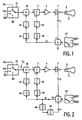
Fig. 1 shows a first embodiment of a display apparatus including a black level setting circuit in accordance with the present invention; -
Fig. 2 shows a second embodiment of a display apparatus including a black level setting circuit in accordance with the present invention; and -
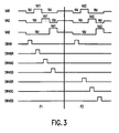
Fig. 3 illustrates some waveforms occurring in the black level setting circuit ofFigs. 1 and 2 . - In the display apparatus of
Fig. 1 , an input video signal Vin is applied to aswitch 42, whose output is connected to acathode 9 of a display device D thru a gain control circuit (e.g. a multiplier) 35, a level control circuit (e.g. an adder) 3, abuffer circuit 5, and avideo output stage 7. Ameasuring circuit 15 subtracts a reference signal received from aswitch 47, from a signal related to the output current Ik supplied to thecathode 9 and received from thevideo output stage 7. An error current Ie from themeasuring circuit 15 is applied to integrators (e.g. capacitors) 43 and 44thru switches control circuits integrators switches - Calibration occurs in two phases. In a first phase of the calibration state, which occurs during a few measuring lines in a first field F1, a first control voltage Vd1 is supplied to the circuit by the
switch 42, and a first reference current Iref1 is applied to themeasuring circuit 15 by theswitch 47. Moreover,switch 46 is closed. After some time, the cathode current Ik will have become equal to Irefl, so that the error current Ie is zero. In a second phase of the calibration state, which occurs during a few measuring lines in a second field F2, a second control voltage Vd2 is supplied to the circuit by theswitch 42, and a second reference current Iref2 is applied to themeasuring circuit 15 by theswitch 47. Moreover,switch 45 is closed (switch 46 is open). After some time, the cathode current Ik will have become equal to Iref2, so that the error current Ie is zero. The calibration is effected during several iterations of the calibration cycle formed by the first phase followed by the second phase, because of the mutual influence of gain control and level control. - Just like in the prior art black level setting of
US-A-5,278,476 , two measurement voltages are applied to the cathode. By observing the ratio between the resulting measured cathode currents, the black level is set at the cut-off point of the cathode ray tube (CRT). Moreover, the gain of the video signal applied to the cathode is controlled. As only two measurements are carried out, the factor γ of the cathode must be known. For usual CRTs this means no limitation because the factor γ is approximately constant (γ = 2.25). New in the present invention is that for an accurate gain control, it is no longer necessary that the level shifts and gain factors of theamplifiers - The ratios between the drive voltages Vd1 and Vd2 and the reference currents Iref1 and Iref2 follow from the observation that for a correctly set black level it holds that (Vd1/Vd2)γ = Iref1/Iref2. To guarantee convergence of the iterative control, Vd2 should exceed Vd1. In a preferred embodiment, Vd1/Vd2 = 213, and Iref1/Iref2 = 2/5, which ratios can easily be realized. When γ = 2.25, only a small error is made. The ratio to be selected between Vd1 and Iref1 (or between Vd2 and Iref2) depends on the desired gain of the transfer function. After calibration, the transfer function is given by: Ik = Iref1,2 * (Vin/Vd1,2)γ. The absolute values of Vd1,2 and Iref1,2 do not influence the black level or the gain. In the embodiment, a compromise has been sought between interference-susceptibility (which determines the minimum values of Vd1,2 and Iref1,2) and visibility of the measurement lines (which determine the maximum values of Vd1,2 and Irefl,2).
- In a color display system, there are three sets of
circuits measuring circuit 15 and only oneswitch 47 are needed because the three cathode currents are taken together. Consequently, the three cathodes can not be calibrated together, but must be calibrated during successive measuring lines as will be illustrated by means ofFig. 3 . - In the embodiment of
Fig. 2 , anarrangement 48, 49 is present in addition to the elements ofFig. 1 , to compensate for leakage currents and for line frequency interference currents to the cathode connections. Theswitches 42 apply blanking voltages Vbl so that no current is applied to the cathodes. Theswitch 47 is in the position shown. The switch 48 is closed, so that the error current Ie is integrated byintegrator 49 to set a compensation current Ic which compensates for all leakage and interference currents. After opening switch 48, theintegrator 49 maintains the compensation current Ic. The measuringcircuit 15 subtracts the compensation current Ic from the difference between the cathode current Ik and the reference current Iref1,2. -
Fig. 3 illustrates a complete calibration cycle. In the first field F1, in one of the first image lines the blanking voltage Vbl is offered to all threecathodes 9. Var indicates the voltage applied to the red channel of the circuit, Vag indicates the voltage applied to the green channel, and Vab indicates the voltage applied to the blue channel. The total leakage / interference current is measured and compensated for by closing switch 48 during this image line (see line SW48 inFig. 3 ). During the next image line, the red channel is calibrated: itsswitch 46 is closed (see line SW46R inFig. 3 ), and the control voltage Vd1 is supplied by itsswitch 42. In the other channels, the blanking voltage Vbl is supplied by theirrespective switches 42 so that the green and blue cathode currents do not influence calibration in the red channel. During the next image line, the green channel is calibrated: itsswitch 46 is closed (see line SW46G inFig. 3 ). During the fourth image line used for calibration, the blue channel is calibrated: itsswitch 46 is closed (see line SW46B inFig. 3 ). The second phase which is carried out during a subsequent field F2, resembles the first phase to a large extent. Instead of switches 46R, 46G and 46B, switches 45R, 45G and 45B are successively closed during the second, third and fourth image lines used for calibration. - It should be noted that the above-mentioned embodiments illustrate rather than limit the invention, and that those skilled in the art will be able to design many alternative embodiments without departing from the scope of the appended claims. For example, three control values and three reference values may be used to obtain a γ-independent control. In the claims, any reference signs placed between parentheses shall not be construed as limiting the claim. The invention can be implemented by means of hardware comprising several distinct elements, and by means of a suitably programmed computer.
Claims (7)
- Black level and gain control setting device for a display device comprising a cathode, comprising:means (42) adapted to apply at least two differing control values (Vd1, Vd2);means (35, 3, 7, 15) adapted to control a black level and gain in response to the at least two differing control values (Vd1, Vd2);means (47) adapted to apply at least two differing reference values (Iref1, Iref2),characterized by
first means (43) adapted to integrate a first error value (Ie) depending on the first control value (Vd1) and the first reference value (Iref1) to obtain a cathode current (Ik) equal to the first reference value (Iref1); and
second means (44) adapted to integrate a second error value (Ie) depending on the second control value (Vd2) and the second reference value (Iref2) to obtain a cathode current (Ik) equal to the second reference value (Iref2),
wherein the at least two differing control values (Vd1, Vd2) are two mutually differing control values (Vd1, Vd2) in a first predetermined ratio, the differing reference values (Iref1, Iref2) are at least two mutually differing reference values (Iref1, Iref2) in a second predetermined ratio and correspond to the at least two mutually differing control values (Vd1, Vd2) provided to the controlling means (35, 3, 7, 15) and a predetermined relationship exists between the first predetermined ratio and the second predetermined ratio. - A black level and gain control setting device as claimed in claim 1, further comprising:third means (49) for integrating a third error value corresponding to leakage and/or interference currents, to obtain a compensation value (Ic) for compensating said controlling means (35, 3, 7, 15) for leakage and/or interference currents.
- A black level and gain control setting device as claimed in claim 1, wherein said first control value (Vd1) and said first reference value (Iref1) are applied (42, 47), and said first error value is integrated (43), during a first calibration phase (F1), and wherein said second control value (Vd2) and said second reference value (Iref2) are applied (42, 47), and said second error value is integrated (44), during a second calibration phase (F2).
- A black level and gain control setting device as claimed in claim 1, wherein said predetermined relationship between said first predetermined ratio (Vd1/Vd2) and said second predetermined ratio(Irefl/iref2) is given by:(Vd1/Vd2)γ=Iref1/lref2.
- A black level and gain control setting device as claimed in claim 4, wherein said first predetermined ratio(Vdl/Vd2) is given by Vd1/Vd2 = 2/3 and said second predetermined ratio(lref1 /lref2) is given by Iref1/Iref2 = 2/5.
- A method of black level and gain control setting, comprising the steps of:applying (42) at least two mutually differing control values (Vd1, Vd2) in a first predetermined ratio;controlling (35, 3, 7, 15) the black level and gain in response to said at least two mutually differing control values (Vd1, Vd2);characterized by:applying (47) at least two mutually differing reference values (Iref1, Iref2) in a second predetermined ratio and corresponding to said at least two mutually differing control values (Vd1, Vd2) to said controlling step (35, 3, 7, 15), where a predetermined relationship exists between said first predetermined ratio and said second predetermined ratio;integrating (43) a first error value depending on a first control value (Vd1) and a first reference value(Iref1) to obtain a a cathode current (Ik) equal to the first reference value (Iref1); andintegrating (44) a second error value depending on a second control value (Vd2) and a second reference value(Iref2) to obtain a cathode current (Ik) equal to the first reference value (Iref2)..
- A display apparatus, comprising:a display device (D); anda black level and gain control setting device as claimed in claim 1, for providing a cathode current (Ik) to said display device.
Priority Applications (1)
| Application Number | Priority Date | Filing Date | Title |
|---|---|---|---|
| EP97900023A EP0818034B1 (en) | 1996-01-29 | 1997-01-16 | Black level setting |
Applications Claiming Priority (4)
| Application Number | Priority Date | Filing Date | Title |
|---|---|---|---|
| EP96200192 | 1996-01-29 | ||
| EP96200192 | 1996-01-29 | ||
| PCT/IB1997/000016 WO1997028525A2 (en) | 1996-01-29 | 1997-01-16 | Black level setting |
| EP97900023A EP0818034B1 (en) | 1996-01-29 | 1997-01-16 | Black level setting |
Publications (2)
| Publication Number | Publication Date |
|---|---|
| EP0818034A2 EP0818034A2 (en) | 1998-01-14 |
| EP0818034B1 true EP0818034B1 (en) | 2008-07-02 |
Family
ID=8223614
Family Applications (1)
| Application Number | Title | Priority Date | Filing Date |
|---|---|---|---|
| EP97900023A Expired - Lifetime EP0818034B1 (en) | 1996-01-29 | 1997-01-16 | Black level setting |
Country Status (6)
| Country | Link |
|---|---|
| US (1) | US5892337A (en) |
| EP (1) | EP0818034B1 (en) |
| JP (1) | JP4070239B2 (en) |
| KR (1) | KR100429327B1 (en) |
| DE (1) | DE69738797D1 (en) |
| WO (1) | WO1997028525A2 (en) |
Families Citing this family (5)
| Publication number | Priority date | Publication date | Assignee | Title |
|---|---|---|---|---|
| JPH10145807A (en) * | 1996-11-12 | 1998-05-29 | Matsushita Electric Ind Co Ltd | Auto cut-off circuit |
| WO2000019727A1 (en) * | 1998-09-25 | 2000-04-06 | Stmicroelectronics Asia Pacific Pte Ltd | A digital cut-off control loop for tv using speeding and blanking circuits |
| JP2002539491A (en) * | 1999-03-11 | 2002-11-19 | コーニンクレッカ フィリップス エレクトロニクス エヌ ヴィ | Setting the cutoff level |
| JP3844430B2 (en) * | 2001-06-26 | 2006-11-15 | 三菱電機株式会社 | Video signal processing apparatus and video signal processing method |
| JP3722740B2 (en) * | 2001-11-05 | 2005-11-30 | 三菱電機株式会社 | Video processing apparatus and video processing method |
Family Cites Families (2)
| Publication number | Priority date | Publication date | Assignee | Title |
|---|---|---|---|---|
| US4370674A (en) * | 1981-03-03 | 1983-01-25 | Zenith Radio Corporation | Stabilization network for a cathode ray tube |
| US5278476A (en) * | 1991-11-13 | 1994-01-11 | U.S. Philips Corporation | Display device including a black level setting circuit |
-
1997
- 1997-01-16 JP JP52743997A patent/JP4070239B2/en not_active Expired - Fee Related
- 1997-01-16 DE DE69738797T patent/DE69738797D1/en not_active Expired - Lifetime
- 1997-01-16 WO PCT/IB1997/000016 patent/WO1997028525A2/en not_active Ceased
- 1997-01-16 EP EP97900023A patent/EP0818034B1/en not_active Expired - Lifetime
- 1997-01-16 KR KR1019970706922A patent/KR100429327B1/en not_active Expired - Fee Related
- 1997-01-23 US US08/788,734 patent/US5892337A/en not_active Expired - Lifetime
Also Published As
| Publication number | Publication date |
|---|---|
| DE69738797D1 (en) | 2008-08-14 |
| US5892337A (en) | 1999-04-06 |
| KR19980703518A (en) | 1998-11-05 |
| KR100429327B1 (en) | 2004-07-31 |
| EP0818034A2 (en) | 1998-01-14 |
| JPH11503589A (en) | 1999-03-26 |
| JP4070239B2 (en) | 2008-04-02 |
| WO1997028525A3 (en) | 1997-10-02 |
| WO1997028525A2 (en) | 1997-08-07 |
Similar Documents
| Publication | Publication Date | Title |
|---|---|---|
| KR970000851B1 (en) | Video signal processing device | |
| JPH0145276B2 (en) | ||
| JPH06339148A (en) | Color correction device, picture display device using the correction device, white balance adjustment system consisting of the display device, white balance adjustment method and color adjustment method | |
| KR930002609B1 (en) | Brightness and contrast adjusting apparatus | |
| EP0467602B1 (en) | Contrast corrector for video signal | |
| JPS6031427B2 (en) | Video signal processing device | |
| KR100300893B1 (en) | Display device and video signal correction circuit and its correction method | |
| JPH10501944A (en) | Video display system with automatic passive tube bias reactive screen grid power supply | |
| US5892337A (en) | Black level setting | |
| US5278476A (en) | Display device including a black level setting circuit | |
| US6295100B1 (en) | Method and device for convergence correction in a television receiver | |
| US4733227A (en) | Color display with automatic color control device | |
| FI76466B (en) | AUTOMATIC STATION SYSTEM FOR SPEAKING AND PIPELINE COMPENSATION FOR PASSENGER STANDARDS AND LED CONDITIONS FOR ELECTRICAL EQUIPMENT. | |
| US4751566A (en) | Method and device for gamma correction in multichrome cathode ray tubes | |
| EP0598442B1 (en) | Display device including a correction circuit, and correction circuit for use in said device | |
| US6563496B1 (en) | Cut-off adjusting apparatus | |
| KR100326994B1 (en) | Voltage Change Compensator for Sample-Hold Capacitors | |
| US5396296A (en) | Video feedback matching circuit and method therefor | |
| US5345151A (en) | Automatic calibration in a waveform generator for deflection | |
| US5410223A (en) | Display device including a black level setting circuit | |
| US6433827B1 (en) | Measurement-free G2 calibration of color picture tubes | |
| JP2970175B2 (en) | White balance control device | |
| EP0605921B1 (en) | Display device including a black level setting circuit | |
| JP2563373B2 (en) | Gamma correction circuit | |
| KR100238807B1 (en) | Automatic Back Balance Adjuster of Image Output Device |
Legal Events
| Date | Code | Title | Description |
|---|---|---|---|
| PUAI | Public reference made under article 153(3) epc to a published international application that has entered the european phase |
Free format text: ORIGINAL CODE: 0009012 |
|
| AK | Designated contracting states |
Kind code of ref document: A2 Designated state(s): DE FR GB IT |
|
| 17P | Request for examination filed |
Effective date: 19980209 |
|
| 17Q | First examination report despatched |
Effective date: 20070122 |
|
| RAP1 | Party data changed (applicant data changed or rights of an application transferred) |
Owner name: NXP B.V. |
|
| GRAP | Despatch of communication of intention to grant a patent |
Free format text: ORIGINAL CODE: EPIDOSNIGR1 |
|
| GRAS | Grant fee paid |
Free format text: ORIGINAL CODE: EPIDOSNIGR3 |
|
| GRAA | (expected) grant |
Free format text: ORIGINAL CODE: 0009210 |
|
| AK | Designated contracting states |
Kind code of ref document: B1 Designated state(s): DE FR GB IT |
|
| REG | Reference to a national code |
Ref country code: GB Ref legal event code: FG4D |
|
| REF | Corresponds to: |
Ref document number: 69738797 Country of ref document: DE Date of ref document: 20080814 Kind code of ref document: P |
|
| PLBE | No opposition filed within time limit |
Free format text: ORIGINAL CODE: 0009261 |
|
| STAA | Information on the status of an ep patent application or granted ep patent |
Free format text: STATUS: NO OPPOSITION FILED WITHIN TIME LIMIT |
|
| 26N | No opposition filed |
Effective date: 20090403 |
|
| PG25 | Lapsed in a contracting state [announced via postgrant information from national office to epo] |
Ref country code: IT Free format text: LAPSE BECAUSE OF FAILURE TO SUBMIT A TRANSLATION OF THE DESCRIPTION OR TO PAY THE FEE WITHIN THE PRESCRIBED TIME-LIMIT Effective date: 20080702 |
|
| REG | Reference to a national code |
Ref country code: FR Ref legal event code: TP Owner name: TRIDENT MICROSYSTEMS (FAR EAST) LTD., KY Effective date: 20120418 |
|
| REG | Reference to a national code |
Ref country code: DE Ref legal event code: R082 Ref document number: 69738797 Country of ref document: DE Representative=s name: EPPING HERMANN FISCHER, PATENTANWALTSGESELLSCH, DE |
|
| REG | Reference to a national code |
Ref country code: DE Ref legal event code: R082 Ref document number: 69738797 Country of ref document: DE Representative=s name: EPPING HERMANN FISCHER, PATENTANWALTSGESELLSCH, DE Effective date: 20121023 Ref country code: DE Ref legal event code: R081 Ref document number: 69738797 Country of ref document: DE Owner name: ENTROPIC COMMUNICATIONS, INC., SAN DIEGO, US Free format text: FORMER OWNER: TRIDENT MICROSYSTEMS (FAR EAST) LTD., GRAND CAYMAN, KY Effective date: 20121023 Ref country code: DE Ref legal event code: R081 Ref document number: 69738797 Country of ref document: DE Owner name: ENTROPIC COMMUNICATIONS, INC., US Free format text: FORMER OWNER: TRIDENT MICROSYSTEMS (FAR EAST) LTD., GRAND CAYMAN, KY Effective date: 20121023 |
|
| REG | Reference to a national code |
Ref country code: FR Ref legal event code: TP Owner name: ENTROPIC COMMUNICATIONS, INC., US Effective date: 20131119 |
|
| PGFP | Annual fee paid to national office [announced via postgrant information from national office to epo] |
Ref country code: DE Payment date: 20140129 Year of fee payment: 18 |
|
| PGFP | Annual fee paid to national office [announced via postgrant information from national office to epo] |
Ref country code: FR Payment date: 20140117 Year of fee payment: 18 |
|
| PGFP | Annual fee paid to national office [announced via postgrant information from national office to epo] |
Ref country code: GB Payment date: 20140127 Year of fee payment: 18 |
|
| REG | Reference to a national code |
Ref country code: DE Ref legal event code: R119 Ref document number: 69738797 Country of ref document: DE |
|
| GBPC | Gb: european patent ceased through non-payment of renewal fee |
Effective date: 20150116 |
|
| PG25 | Lapsed in a contracting state [announced via postgrant information from national office to epo] |
Ref country code: DE Free format text: LAPSE BECAUSE OF NON-PAYMENT OF DUE FEES Effective date: 20150801 Ref country code: GB Free format text: LAPSE BECAUSE OF NON-PAYMENT OF DUE FEES Effective date: 20150116 |
|
| REG | Reference to a national code |
Ref country code: FR Ref legal event code: ST Effective date: 20150930 |
|
| PG25 | Lapsed in a contracting state [announced via postgrant information from national office to epo] |
Ref country code: FR Free format text: LAPSE BECAUSE OF NON-PAYMENT OF DUE FEES Effective date: 20150202 |