EP0817542B1 - Discharge lamp lighting device - Google Patents
Discharge lamp lighting device Download PDFInfo
- Publication number
- EP0817542B1 EP0817542B1 EP97900125A EP97900125A EP0817542B1 EP 0817542 B1 EP0817542 B1 EP 0817542B1 EP 97900125 A EP97900125 A EP 97900125A EP 97900125 A EP97900125 A EP 97900125A EP 0817542 B1 EP0817542 B1 EP 0817542B1
- Authority
- EP
- European Patent Office
- Prior art keywords
- discharge lamp
- waveform
- voltage
- lamp
- gas
- Prior art date
- Legal status (The legal status is an assumption and is not a legal conclusion. Google has not performed a legal analysis and makes no representation as to the accuracy of the status listed.)
- Revoked
Links
Images






Classifications
-
- H—ELECTRICITY
- H05—ELECTRIC TECHNIQUES NOT OTHERWISE PROVIDED FOR
- H05B—ELECTRIC HEATING; ELECTRIC LIGHT SOURCES NOT OTHERWISE PROVIDED FOR; CIRCUIT ARRANGEMENTS FOR ELECTRIC LIGHT SOURCES, IN GENERAL
- H05B41/00—Circuit arrangements or apparatus for igniting or operating discharge lamps
- H05B41/14—Circuit arrangements
- H05B41/26—Circuit arrangements in which the lamp is fed by power derived from DC by means of a converter, e.g. by high-voltage DC
- H05B41/28—Circuit arrangements in which the lamp is fed by power derived from DC by means of a converter, e.g. by high-voltage DC using static converters
- H05B41/2806—Circuit arrangements in which the lamp is fed by power derived from DC by means of a converter, e.g. by high-voltage DC using static converters with semiconductor devices and specially adapted for lamps without electrodes in the vessel, e.g. surface discharge lamps, electrodeless discharge lamps
-
- H—ELECTRICITY
- H05—ELECTRIC TECHNIQUES NOT OTHERWISE PROVIDED FOR
- H05B—ELECTRIC HEATING; ELECTRIC LIGHT SOURCES NOT OTHERWISE PROVIDED FOR; CIRCUIT ARRANGEMENTS FOR ELECTRIC LIGHT SOURCES, IN GENERAL
- H05B41/00—Circuit arrangements or apparatus for igniting or operating discharge lamps
- H05B41/14—Circuit arrangements
- H05B41/24—Circuit arrangements in which the lamp is fed by high frequency AC, or with separate oscillator frequency
-
- Y—GENERAL TAGGING OF NEW TECHNOLOGICAL DEVELOPMENTS; GENERAL TAGGING OF CROSS-SECTIONAL TECHNOLOGIES SPANNING OVER SEVERAL SECTIONS OF THE IPC; TECHNICAL SUBJECTS COVERED BY FORMER USPC CROSS-REFERENCE ART COLLECTIONS [XRACs] AND DIGESTS
- Y02—TECHNOLOGIES OR APPLICATIONS FOR MITIGATION OR ADAPTATION AGAINST CLIMATE CHANGE
- Y02B—CLIMATE CHANGE MITIGATION TECHNOLOGIES RELATED TO BUILDINGS, e.g. HOUSING, HOUSE APPLIANCES OR RELATED END-USER APPLICATIONS
- Y02B20/00—Energy efficient lighting technologies, e.g. halogen lamps or gas discharge lamps
Definitions
- the invention relates to a device for operating a fluorescent discharge lamp according to the preamble of claim 1.
- EP 0593312 A discloses a fluorescent light source having a twin tube and inner filament cathodes at opposite ends.
- a fluorescent discharge lamp of the outer electrode type is known as a fluorescent lamp which is used for document scanning illumination of an office automation device and for back light of a liquid crystal display of an office automation device and the like.
- Figure 12 is a schematic of an arrangement of the above described fluorescent discharge lamp of the outer electrode type.
- Figure 12 (a) shows a cross section of the fluorescent discharge lamp of the outer electrode type which corresponds to the direction perpendicular to the direction of the tube axis.
- Figure 12 (b) is a side view hereof.
- fluorescent discharge lamp of the outer electrode type 1 consists of discharge vessel 3 which consists of a dielectric such as glass or the like, a pair of strip-like or line-like electrodes 2, 2', and layers of fluorescent material 4 which are formed on the inside of discharge vessel 3. Electrodes 2, 2' are located on the side of discharge vessel 3 in the direction of the tube axis roughly over the entire length and consist of aluminum or the like.
- above described fluorescent discharge lamp of the outer electrode type 1 has been operated by applying a high frequency voltage to the outer electrodes as in a cold cathode fluorescent discharge lamp of the inner electrode type. That is, high frequency main circuit 5 as shown in Figure 13 is connected to the pair of electrodes 2, 2' of fluorescent discharge lamp of the outer electrode type 1. For example, a waveform high frequency AC voltage according to Figure 14 is applied to electrodes 2, 2'. In this way a high frequency voltage is applied in the discharge space within discharge vessel 3 which is present between outer electrodes 2, 2' via the side discharge vessel 3, forming a discharge.
- Fluorescent discharge lamp of the outer electrode type 1 shown in Figure 12 can be called a capacitor which consists of outer electrodes 2, 2' and discharge vessel 3 as the dielectric.
- the lamp current which is supplied to this fluorescent discharge lamp of the outer electrode type 1 is determined by the magnitude of electrostatic capacity which is formed between outer electrodes 2, 2' and discharge vessel 3 which consists of the dielectric.
- Current must be supplied to increase the illuminance of fluorescent discharge lamp of the outer electrode type 1 even more. This means that the voltage applied to outer electrodes 2, 2' and the high frequency of the voltage must be increased.
- the invention is devised to eliminate the above described disadvantage. Therefore the object of the invention is to devise a device for operating a fluorescent discharge lamp of the outer electrode type in which even when the pressure of the filled gas is increased in the discharge vessel a stable discharge can be maintained and in which at the same time higher illuminance can be obtained.
- the arrangement described above in (1) to (7) makes it possible to maintain a stable discharge even when the pressure of the gas filled in the discharge lamp is increased, and to further increase the illuminance more than in the conventional operation method in which the sine curve is applied.
- FIG. 1 is a schematic of an arrangement of a basic circuit of one embodiment of the device as claimed in the invention for operating fluorescent discharge lamp 1 of the outer electrode type (hereinafter called a discharge lamp). Furthermore, reference number 6 labels a DC source, reference number 7 a driver circuit, reference number 8 a switching device, and reference number 9 a transformer. This figure shows the arrangement of a basic circuit of the fly-back type. Switching device 8 is turned on and off by driver signals with a stipulated frequency which is delivered by driver circuit 7. If switching device 8 is turned on by the above described driver signals, current flows via a line from DC source 6 via the primary winding of transformer 9, switching device 8 to ground G, and energy is stored in transformer 9.
- a discharge lamp the outer electrode type
- discharge vessel 3 consisting of glass or the like does not in fact act as a dielectric, and thus an approximation to a state is achieved in which a voltage is applied directly to the gas filled inside.
- the latter is a dielectric. If a voltage is applied to the lamp, this glass surface is therefore electrified and discharge begins if a breakdown voltage is achieved. This discharge immediately neutralizes the glass surface and then stops because there is no longer any potential gradient. When the next discharge begins, the glass surface is neutralized again and the discharge stopped in the same way. This process is repeated. This phenomenon arises depending on the condition of the glass surface and the respective electrification condition in each area of the glass surface..
- the illumination intensity of the ultraviolet radiation which are emitted from the Xe gas of discharge lamp 1 decreases both at an overly high repetition frequency of the above described voltage applied to discharge lamp 1 (called the "operation frequency"), and also at an overly low operation frequency.
- operation frequency an overly high repetition frequency of the above described voltage applied to discharge lamp 1
- the discharge lamp is operated in a stable emission condition even if the pressure of the filled gas is increased.
- FIG 2 is a schematic of an arrangement of a circuit of the flyback type of another embodiment of the operation device as claimed in the invention.
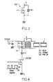
- diode D is located in series with switching device 8. If for example a MOSFET is used as switching device 8, conventionally with respect to an arrangement between the drain and the source electrode there is diode D1, as is shown in Figure 3.
- a MOSFET is used as switching device 8
- diode D1 conventionally with respect to an arrangement between the drain and the source electrode there is diode D1
- the circuit shown in Figure 2 therefore at the instant the input power is turned off on the primary side of transformer 9 an electromotive counterforce is formed, the current flowing in the direction of arrow in Figure 3 and the efficiency decreasing to a high degree.
- diode D is series connected to switching device 8 so that the above described current is hindered. Without a decrease of efficiency, this arrangement yields a voltage waveform with above described full width at half maximum within a stipulated value even if switching decive 8 which is shown in Figure 3 and which is provided with diode D1 is used.
- FIG 4 is a schematic of one arrangement of an experimental circuit of the flyback type which was used in this embodiment.
- a MOSFET was used as switching device 8.
- Diode D was series connected to switching device 8, as was shown in Figure 2.
- snubber circuit 10 is connected; it consists of a series connection of resistor R1 of 50 ohms and capacitor C1 of 1000 pF.
- a 24 V DC source was connected to one of the terminals on the primary side of transformer 9, while switching device 8 was connected to the other terminal via diode D and was supplied with driver signals with a peak value of 12 V, as is shown in the drawing.
- Capacitor C2 of 440 ⁇ F was connected to the 24 V DC source.
- Transformer 9 with following properties (1) to (4) was used, the full width at half maximum of the periodic voltage waveform which is formed on the secondary side of transformer 9 having been changed.
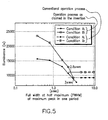
- Figures 5 and 6 are schematics of the relation between the full width at half maximum which was obtained in the above described experimental circuit, and the illuminance of the discharge lamp.
- a lamp with a tube diameter of 8 mm and a lamp length of 360 mm is used as a discharge lamp; it has two strip-like electrodes (one pair) with an electrode width of 8 mm.
- Figure 5 shows the relation between the full width at half maximum and the illuminance during operation of the discharge lamp under conditions A and B described below.
- the "operation process as claimed in the invention” represents operation using the circuit shown in Figure 4, while the “conventional operation process” represents operation of the discharge lamp with a sine curve high frequency AC voltage.
- Operation in the operation process as claimed in the invention was accomplished with a operation frequency of 40 kHz under condition A and with a operation frequency of 70 kHz under condition B.
- the illumination intensity under conditions A and B is essentially constant, regardless of the value of the full width at half maximum.
- the illuminance becomes higher according to a reduction of the full width at half maximum.
- the illuminance at a full width at half maximum of less than 2.8 ⁇ s to 3 ⁇ s becomes higher than in the conventional light operation process.
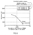
- a lamp with a tube diameter of 6.5 mm and a lamp length of 360 mm is used as a discharge lamp; it has two strip-like electrodes (one pair) with an electrode width of 7 mm.
- Figure 6 shows the relation between the full width at half maximum and the illuminance during operation of the discharge lamp under the same condition as above described condition B, i.e., with a lamp wattage of 13 W.
- the "operation process as claimed in the invention” represents operation using the circuit shown in Figure 4, while the “conventional operation process” represents operation of the discharge lamp with a sine curve high frequency AC voltage, as in Figure 5.
- the operation frequency in the operation process as claimed in the invention was 70 kHz.
- the lamp wattage for example at a peak voltage of 1400 V was 13.5 W for waveform 1, 12.7 W for waveform 2 and 11.0 W for waveform 3. This corresponds to 1.22 for waveform 1 and 1.14 for waveform 2 if the lamp wattage is designated 1 for waveform 3.
- These differences of lamp wattage are based on differences of the power which is supplied to the oscillation wave which follows on the maximum peak voltage and which contributes to emission.
- Figure 8 schematically shows the relation between the lamp wattage and the illuminance if the above described waveforms 1 through 3 have been applied to the discharge lamp.
- a lamp with a tube diameter of 8 mm and a lamp length of 360 mm is used as a discharge lamp, the operation frequency being 70 kHz.
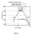
- Figure 9 is a schematic of the relation between the operation period and the illuminance (lamp wattage is constant: 13 W).
- the "operation process as claimed in the invention” represents operation using the circuit shown in Figure 4, while the “conventional operation process” represents luminous operation of the discharge lamp with a sine curve high frequency AC voltage, as in Figure 5.
- a discharge lamp with a tube diameter of 8 mm and a lamp length of 360 mm was used.
- the illuminance decreases in the "operation process as claimed in the invention" when the operation period becomes longer. For a short operation period the illuminance also decreases.
- the conceivable reason for this is that at a low operation frequency (for a long operation period) the radiant efficiency and illuminance decrease and that for an overly high operation frequency (for a short operation period) emission with good radiant efficiency from the excitation species cannot take place, as was described above.
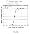
- Figure 10 is a schematic of the relation between the partial pressure of the Xe gas and the relative luminance fluctuation.
- operation process as claimed in the invention represents operation using the circuit shown in Figure 4, while the “conventional operation process” represents operation of the discharge lamp with a sine curve, as shown in Figure 5.
- a discharge lamp with a tube diameter of 8 mm and a lamp length of 360 mm was used which was operated at lamp wattage of 13 W. Three minutes after starting operation relative luminance fluctuation was determined.
- the filling pressure of the Xe gas can be set to greater than or equal to 10665,79 N/m 2 (80 torr), at which a stable luminous condition could not be easily maintained in the "conventional operation process" due to high brightness control. As claimed in the invention, this enabled a higher illuminance to be maintained than in the "conventional operation process".
- Figure 11 schematically shows the efficiency of the illuminance when the mixing ratio of Ne gas changes, the Xe gas pressure having been 13332,24 N/m 2 (100 torr) using the above described basis of gases.
- a discharge lamp with a tube diameter of 8 mm, a lamp length of 360 mm, an operation frequency of 70 kHz and constant lamp wattage of 20 W was used.
- the efficiency of the illuminance increases when the mixing ratio of the Ne gas is increased as the partial pressure of the Xe gas is kept at 13332,24 N/m 2 (100 torr).
- the total pressure within the discharge lamp is 66661,20 N/m 2 (500 torr). If however the total pressure of filling in the discharge lamp is greater than or equal to 101325,02 N/m 2 (760 torr), the difficulty arises that when the discharge lamp is produced the lamp expands, making its manufacture difficult. It is therefore desirable that the total pressure of the gas encapsulated in the discharge lamp be less than or equal to 101325,02 N/m 2 (760 torr).
- the device for operating a discharge lamp can be used for document scanning illumination of an information processing device, such as a fax machine, a copier, an image reader and the like, and for a background light device of a liquid crystal display.
Landscapes
- Circuit Arrangements For Discharge Lamps (AREA)
- Discharge Lamps And Accessories Thereof (AREA)
- Discharge Lamp (AREA)
- Vessels And Coating Films For Discharge Lamps (AREA)
Description
- Fig. 1
- shows a schematic of one arrangement of a basic circuit of the flyback type of one embodiment of the device as claimed in the invention for operating a discharge lamp;
- Fig. 2
- shows a schematic of an arrangement of a circuit of the flyback type of another embodiment of the operation device as claimed in the invention;
- Fig. 3
- shows a schematic of one arrangement of a MOSFET circuit intrinsically including one diode;
- Fig. 4
- shows a schematic of one arrangement of an experimental circuit of the flyback type which is used in the invention;
- Fig. 5
- shows a schematic of the relation between the full width at half maximum and the illuminance of the discharge lamp (with 8 mm diameter);
- Fig. 6
- shows a schematic of the relation between the full width at half maximum and the illuminance of the discharge lamp (with 6.5 mm diameter);
- Fig. 7 (a)
- through Figure 7 (d) each show one schematic of the lamp voltage waveform in operation of the discharge lamp;
- Fig. 8
- shows a schematic of the relation between the lamp wattage and the illuminance with different waveforms;
- Fig. 9
- shows a schematic of the relation between the operation period and the illuminance;
- Fig. 10
- shows a schematic of the relation between the partial pressure of the Xe gas and the relative luminance fluctuation;
- Fig. 11
- shows a schematic of the relation between the mixing ratio of Ne and the illuminance;
- Fig. 12 (a)
- shows a schematic cross section of one arrangement of a fluorescent discharge lamp of the outer electrode type as disclosed in US 5117 160 A; and
- Fig. 12 (b)
- shows a schematic side view of the arrangement according to Figure 12 (a);
- Fig. 13
- shows a schematic of a circuit of a conventional operation type using a sine curve high frequency of a fluorescent discharge lamp of the outer electrode type;
- Fig. 14
- shows a schematic of a voltage waveform for operation of a conventional fluorescent discharge lamp of the outer electrode type; and
- Fig. 15
- shows a schematic of a pnenomenon of unstable discharge which occurs at a high pressure of the filled gas.
- Condition A:
- lamp wattage 7 W
- Condition B:
- lamp wattage 13W
Claims (4)
- Device for operating a fluorescent discharge lamp for document scanning illumination of an information processing device and for a background light device of a liquid crystal display, in which within a glass tube (3) at least one of the rare gases He, Ne, Ar, Kr, or Xe is hermetically sealed in a stipulated amount, in which fluorescent material is applied to the inside of the glass tube (3), and in which in the axial direction on the outside of the glass tube (3) there are at least two strip-shaped electrodes (2) over the entire length of the glass tube (3), and with a lamp voltage with a cyclic voltage waveform, controlled by a driver circuit(7),
characterized in thatthe driver circuit (7) is of the fly-back type,in the cyclic voltage waveform the zero-level width Wo of the waveform having the maximum peak voltage in one period is set to 2 Wo < t with respect to the cycle period t, whereby a half-value width W is set to a predetermined value of a waveform in the range of 10 µs ≤ t ≤ 30 µs,all electrodes (2)are arranged on the outside of the glass tube (3)
and there are no inner electrodes (Fig.1). - Device for operating a fluorescent discharge lamp according to claim 1,
wherein in the cyclic voltage waveform the half maximum level width W of the waveform having the maximum peak value is set in the range of W ≤ 2.5 µs (Fig.5). - Device for operating a fluorescent discharge lamp according to claim 1 or 2,
wherein the glass tube (3) of the fluorescent discharge lamp of the outer electrode type (1) comprises a gas with a partial pressure of the Xe gas of greater than or equal to 10 665,79 N/m2 (80 torr) and a total pressure of the filled gas of less than or equal to 101 325,02 N/m2 (760 torr). - Device for operating a fluorescent discharge lamp according to one of the proceeding claims,
wherein an oscillation wave which follows the maximum peak voltage is supplied with an effective power which contributes to emission.
Applications Claiming Priority (4)
| Application Number | Priority Date | Filing Date | Title |
|---|---|---|---|
| JP449996 | 1996-01-16 | ||
| JP00449996A JP3277788B2 (en) | 1996-01-16 | 1996-01-16 | Discharge lamp lighting device |
| JP4499/96 | 1996-01-16 | ||
| PCT/JP1997/000044 WO1997026779A1 (en) | 1996-01-16 | 1997-01-13 | Discharge lamp lighting device |
Publications (3)
| Publication Number | Publication Date |
|---|---|
| EP0817542A1 EP0817542A1 (en) | 1998-01-07 |
| EP0817542A4 EP0817542A4 (en) | 1998-04-29 |
| EP0817542B1 true EP0817542B1 (en) | 2002-03-27 |
Family
ID=11585763
Family Applications (1)
| Application Number | Title | Priority Date | Filing Date |
|---|---|---|---|
| EP97900125A Revoked EP0817542B1 (en) | 1996-01-16 | 1997-01-13 | Discharge lamp lighting device |
Country Status (9)
| Country | Link |
|---|---|
| US (1) | US5977722A (en) |
| EP (1) | EP0817542B1 (en) |
| JP (1) | JP3277788B2 (en) |
| KR (1) | KR100436884B1 (en) |
| CN (1) | CN1155298C (en) |
| CA (1) | CA2215599C (en) |
| DE (1) | DE69711278T2 (en) |
| TW (1) | TW344188B (en) |
| WO (1) | WO1997026779A1 (en) |
Families Citing this family (19)
| Publication number | Priority date | Publication date | Assignee | Title |
|---|---|---|---|---|
| JP3355976B2 (en) * | 1997-02-05 | 2002-12-09 | ウシオ電機株式会社 | Discharge lamp lighting device |
| US6323600B1 (en) * | 1997-07-22 | 2001-11-27 | Patent-Treuhand-Gesellschaft Fuer Elektrische Gluehlampen Mbh | Process for generating voltage pulse sequences and circuit assembly therefor |
| DE19734883C1 (en) * | 1997-08-12 | 1999-03-18 | Patent Treuhand Ges Fuer Elektrische Gluehlampen Mbh | Method for generating pulse voltage sequences for the operation of discharge lamps and associated circuit arrangement |
| DE19734885C1 (en) * | 1997-08-12 | 1999-03-11 | Patent Treuhand Ges Fuer Elektrische Gluehlampen Mbh | Method for generating pulse voltage sequences for the operation of discharge lamps and associated circuit arrangement |
| JP3353684B2 (en) * | 1998-01-09 | 2002-12-03 | ウシオ電機株式会社 | Dielectric barrier discharge lamp light source device |
| JP3296284B2 (en) * | 1998-03-12 | 2002-06-24 | ウシオ電機株式会社 | Dielectric barrier discharge lamp light source device and its power supply device |
| DE19839336A1 (en) | 1998-08-28 | 2000-03-09 | Patent Treuhand Ges Fuer Elektrische Gluehlampen Mbh | Electronic ballast for discharge lamp with dielectric barrier discharge |
| DE19839329A1 (en) * | 1998-08-28 | 2000-03-09 | Patent Treuhand Ges Fuer Elektrische Gluehlampen Mbh | Electronic ballast for discharge lamp with dielectric barrier discharge |
| JP2001015287A (en) | 1999-04-30 | 2001-01-19 | Ushio Inc | Dielectric barrier discharge lamp light source device |
| DE69938465T2 (en) * | 1999-10-18 | 2009-06-04 | Ushio Denki K.K. | DIELECTRICALLY DISABLED DISCHARGE LAMP AND LIGHT SOURCE |
| DE10011484A1 (en) | 2000-03-09 | 2001-09-13 | Patent Treuhand Ges Fuer Elektrische Gluehlampen Mbh | Operating method for discharge lamp with dielectric layer between electrode and discharge medium, involves using mains starter with primary circuit and secondary circuit |
| JP3755390B2 (en) * | 2000-09-08 | 2006-03-15 | 株式会社日立製作所 | Phosphor, display device using the same, and light source |
| JP2002289385A (en) * | 2001-03-23 | 2002-10-04 | Harison Toshiba Lighting Corp | Discharge lamp drive |
| JP4293409B2 (en) | 2001-05-25 | 2009-07-08 | ウシオ電機株式会社 | Dielectric barrier discharge lamp lighting device |
| JP2003036987A (en) | 2001-07-24 | 2003-02-07 | Harison Toshiba Lighting Corp | Discharge lamp lighting device, equipment and image forming device |
| US7615931B2 (en) | 2005-05-02 | 2009-11-10 | International Technology Center | Pulsed dielectric barrier discharge |
| GB0611408D0 (en) * | 2006-06-09 | 2006-07-19 | Uv Energy Ltd | Ballast |
| US8598799B2 (en) | 2007-12-19 | 2013-12-03 | Epistar Corporation | Alternating current light emitting device |
| JP2023125954A (en) * | 2022-02-28 | 2023-09-07 | ウシオ電機株式会社 | Light source device |
Family Cites Families (15)
| Publication number | Priority date | Publication date | Assignee | Title |
|---|---|---|---|---|
| JPS61133596A (en) * | 1984-12-03 | 1986-06-20 | 株式会社 ソフア−ド | Lighting for neon sign |
| JP2839251B2 (en) * | 1987-09-28 | 1998-12-16 | ウシオ電機株式会社 | Lighting method of rare gas fluorescent lamp |
| CA2006034C (en) * | 1988-12-27 | 1995-01-24 | Takehiko Sakurai | Rare gas discharge fluorescent lamp device |
| US5072155A (en) * | 1989-05-22 | 1991-12-10 | Mitsubishi Denki Kabushiki Kaisha | Rare gas discharge fluorescent lamp device |
| US5117160C1 (en) * | 1989-06-23 | 2001-07-31 | Nec Corp | Rare gas discharge lamp |
| JP2658506B2 (en) * | 1990-06-06 | 1997-09-30 | 三菱電機株式会社 | Rare gas discharge fluorescent lamp device |
| JPH0817403A (en) * | 1991-03-13 | 1996-01-19 | Toshiba Lighting & Technol Corp | Noble gas discharge lamp |
| JPH0574587A (en) * | 1991-03-31 | 1993-03-26 | Toshiba Lighting & Technol Corp | Rare gas discharge lamp lighting device |
| EP0593312B1 (en) * | 1992-10-16 | 1998-12-23 | Flowil International Lighting (Holding) B.V. | Fluorescent light source |
| JPH06188087A (en) * | 1992-12-15 | 1994-07-08 | Nec Home Electron Ltd | Lighting device for rare gas discharge lamp |
| DE4311197A1 (en) * | 1993-04-05 | 1994-10-06 | Patent Treuhand Ges Fuer Elektrische Gluehlampen Mbh | Method for operating an incoherently radiating light source |
| JPH0794150A (en) * | 1993-07-30 | 1995-04-07 | Toshiba Lighting & Technol Corp | Rare gas discharge lamp and display device using the same |
| JPH08273863A (en) * | 1995-03-31 | 1996-10-18 | Ushio Inc | External electrode type fluorescent discharge tube lighting system |
| US5637965A (en) * | 1995-10-18 | 1997-06-10 | Matsushita Electric Works R&D Laboratory, Inc. | Low pressure sodium-mercury lamp yielding substantially white light |
| DE19548003A1 (en) * | 1995-12-21 | 1997-06-26 | Patent Treuhand Ges Fuer Elektrische Gluehlampen Mbh | Circuit arrangement for generating pulse voltage sequences, in particular for the operation of dielectrically impeded discharges |
-
1996
- 1996-01-16 JP JP00449996A patent/JP3277788B2/en not_active Expired - Lifetime
-
1997
- 1997-01-13 US US08/913,111 patent/US5977722A/en not_active Expired - Lifetime
- 1997-01-13 CA CA002215599A patent/CA2215599C/en not_active Expired - Lifetime
- 1997-01-13 KR KR1019970706434A patent/KR100436884B1/en not_active Expired - Lifetime
- 1997-01-13 DE DE69711278T patent/DE69711278T2/en not_active Expired - Lifetime
- 1997-01-13 EP EP97900125A patent/EP0817542B1/en not_active Revoked
- 1997-01-13 WO PCT/JP1997/000044 patent/WO1997026779A1/en not_active Ceased
- 1997-01-13 CN CNB971900159A patent/CN1155298C/en not_active Expired - Lifetime
- 1997-01-24 TW TW086100778A patent/TW344188B/en not_active IP Right Cessation
Also Published As
| Publication number | Publication date |
|---|---|
| US5977722A (en) | 1999-11-02 |
| TW344188B (en) | 1998-11-01 |
| JPH09199285A (en) | 1997-07-31 |
| KR19980703026A (en) | 1998-09-05 |
| EP0817542A4 (en) | 1998-04-29 |
| DE69711278T2 (en) | 2002-11-21 |
| CA2215599A1 (en) | 1997-07-24 |
| WO1997026779A1 (en) | 1997-07-24 |
| CN1155298C (en) | 2004-06-23 |
| JP3277788B2 (en) | 2002-04-22 |
| EP0817542A1 (en) | 1998-01-07 |
| CN1178062A (en) | 1998-04-01 |
| DE69711278D1 (en) | 2002-05-02 |
| CA2215599C (en) | 2002-05-21 |
| KR100436884B1 (en) | 2004-08-11 |
Similar Documents
| Publication | Publication Date | Title |
|---|---|---|
| US5977722A (en) | Device for applying particular voltage waveform for operating a discharge lamp | |
| US6084360A (en) | Device for operation of a discharge lamp | |
| KR100399243B1 (en) | Discharge lamp and device for operating it | |
| KR940009330B1 (en) | Rare gas discharge fluorescent lamp device | |
| US6614185B1 (en) | Discharge tube with interior and exterior electrodes | |
| US7271546B2 (en) | Lighting device for dielectric barrier discharge lamp | |
| CA2345747C (en) | Dimmable discharge lamp for dielectrically impeded discharges | |
| EP1263266B1 (en) | Device for operating a dielectric barrier discharge lamp | |
| HUP0103743A2 (en) | Dimmable dielectrically impeded discharge lamp and method of its operating | |
| KR20030007063A (en) | Dielectric barrier discharge lamp having a starting aid | |
| JP3540333B2 (en) | Fluorescent lamp device | |
| EP0948030A2 (en) | Rare gaseous discharge lamp, lighting circuit, and lighting device | |
| EP1511365A1 (en) | A lighting device for a dielectric barrier discharge lamp | |
| EP1441574A1 (en) | Discharging lamp apparatus | |
| JPH09312200A (en) | Discharge lamp lighting device | |
| US20050116661A1 (en) | Discharge lamp apparatus | |
| JP2000277056A (en) | Noble gas discharge lamp, rare gas discharge lamp lighting device and lighting device | |
| US20070090768A1 (en) | Lighting device for a discharge lamp | |
| JP2003347081A (en) | Lighting circuit for dielectric barrier discharge lamp and illuminating device | |
| JPH02306596A (en) | Rare gas discharging fluorescent lamp device | |
| JPH11297278A (en) | Rare gas discharge lamp and lighting device thereof | |
| JP2000323289A (en) | Driving method of discharge device | |
| EP1374646A2 (en) | Capacitively coupled fluorescent lamp package | |
| JP2004158467A (en) | Fluorescent lamp device |
Legal Events
| Date | Code | Title | Description |
|---|---|---|---|
| PUAI | Public reference made under article 153(3) epc to a published international application that has entered the european phase |
Free format text: ORIGINAL CODE: 0009012 |
|
| AK | Designated contracting states |
Kind code of ref document: A1 Designated state(s): DE FR GB NL |
|
| 17P | Request for examination filed |
Effective date: 19971211 |
|
| RHK1 | Main classification (correction) |
Ipc: H05B 41/29 |
|
| A4 | Supplementary search report drawn up and despatched |
Effective date: 19980312 |
|
| AK | Designated contracting states |
Kind code of ref document: A4 Designated state(s): DE FR GB NL |
|
| 17Q | First examination report despatched |
Effective date: 19980724 |
|
| GRAG | Despatch of communication of intention to grant |
Free format text: ORIGINAL CODE: EPIDOS AGRA |
|
| GRAG | Despatch of communication of intention to grant |
Free format text: ORIGINAL CODE: EPIDOS AGRA |
|
| GRAH | Despatch of communication of intention to grant a patent |
Free format text: ORIGINAL CODE: EPIDOS IGRA |
|
| GRAH | Despatch of communication of intention to grant a patent |
Free format text: ORIGINAL CODE: EPIDOS IGRA |
|
| GRAH | Despatch of communication of intention to grant a patent |
Free format text: ORIGINAL CODE: EPIDOS IGRA |
|
| REG | Reference to a national code |
Ref country code: GB Ref legal event code: IF02 |
|
| GRAA | (expected) grant |
Free format text: ORIGINAL CODE: 0009210 |
|
| RIC1 | Information provided on ipc code assigned before grant |
Free format text: 7H 05B 41/288 A, 7H 05B 41/24 B |
|
| AK | Designated contracting states |
Kind code of ref document: B1 Designated state(s): DE FR GB NL |
|
| REF | Corresponds to: |
Ref document number: 69711278 Country of ref document: DE Date of ref document: 20020502 |
|
| PLBI | Opposition filed |
Free format text: ORIGINAL CODE: 0009260 |
|
| PLBF | Reply of patent proprietor to notice(s) of opposition |
Free format text: ORIGINAL CODE: EPIDOS OBSO |
|
| 26 | Opposition filed |
Opponent name: OSRAM GMBH Effective date: 20021219 |
|
| NLR1 | Nl: opposition has been filed with the epo |
Opponent name: OSRAM GMBH |
|
| PLBF | Reply of patent proprietor to notice(s) of opposition |
Free format text: ORIGINAL CODE: EPIDOS OBSO |
|
| PLAX | Notice of opposition and request to file observation + time limit sent |
Free format text: ORIGINAL CODE: EPIDOSNOBS2 |
|
| PLAS | Information related to reply of patent proprietor to notice(s) of opposition deleted |
Free format text: ORIGINAL CODE: EPIDOSDOBS3 |
|
| PLBB | Reply of patent proprietor to notice(s) of opposition received |
Free format text: ORIGINAL CODE: EPIDOSNOBS3 |
|
| RDAF | Communication despatched that patent is revoked |
Free format text: ORIGINAL CODE: EPIDOSNREV1 |
|
| APBP | Date of receipt of notice of appeal recorded |
Free format text: ORIGINAL CODE: EPIDOSNNOA2O |
|
| APBQ | Date of receipt of statement of grounds of appeal recorded |
Free format text: ORIGINAL CODE: EPIDOSNNOA3O |
|
| APAH | Appeal reference modified |
Free format text: ORIGINAL CODE: EPIDOSCREFNO |
|
| APBU | Appeal procedure closed |
Free format text: ORIGINAL CODE: EPIDOSNNOA9O |
|
| RDAD | Information modified related to despatch of communication that patent is revoked |
Free format text: ORIGINAL CODE: EPIDOSCREV1 |
|
| APBP | Date of receipt of notice of appeal recorded |
Free format text: ORIGINAL CODE: EPIDOSNNOA2O |
|
| APAH | Appeal reference modified |
Free format text: ORIGINAL CODE: EPIDOSCREFNO |
|
| APBQ | Date of receipt of statement of grounds of appeal recorded |
Free format text: ORIGINAL CODE: EPIDOSNNOA3O |
|
| APAH | Appeal reference modified |
Free format text: ORIGINAL CODE: EPIDOSCREFNO |
|
| PGFP | Annual fee paid to national office [announced via postgrant information from national office to epo] |
Ref country code: FR Payment date: 20120202 Year of fee payment: 16 |
|
| PGFP | Annual fee paid to national office [announced via postgrant information from national office to epo] |
Ref country code: DE Payment date: 20120111 Year of fee payment: 16 |
|
| PGFP | Annual fee paid to national office [announced via postgrant information from national office to epo] |
Ref country code: GB Payment date: 20120111 Year of fee payment: 16 |
|
| PLBP | Opposition withdrawn |
Free format text: ORIGINAL CODE: 0009264 |
|
| PGFP | Annual fee paid to national office [announced via postgrant information from national office to epo] |
Ref country code: NL Payment date: 20120125 Year of fee payment: 16 |
|
| REG | Reference to a national code |
Ref country code: DE Ref legal event code: R103 Ref document number: 69711278 Country of ref document: DE Ref country code: DE Ref legal event code: R064 Ref document number: 69711278 Country of ref document: DE |
|
| APBU | Appeal procedure closed |
Free format text: ORIGINAL CODE: EPIDOSNNOA9O |
|
| RDAG | Patent revoked |
Free format text: ORIGINAL CODE: 0009271 |
|
| STAA | Information on the status of an ep patent application or granted ep patent |
Free format text: STATUS: PATENT REVOKED |
|
| 27W | Patent revoked |
Effective date: 20120731 |
|
| GBPR | Gb: patent revoked under art. 102 of the ep convention designating the uk as contracting state |
Effective date: 20120731 |
|
| REG | Reference to a national code |
Ref country code: DE Ref legal event code: R107 Ref document number: 69711278 Country of ref document: DE Effective date: 20130307 |