EP0817301B1 - Input coupling adjustment arrangement for radio frequency filters - Google Patents
Input coupling adjustment arrangement for radio frequency filters Download PDFInfo
- Publication number
- EP0817301B1 EP0817301B1 EP97110682A EP97110682A EP0817301B1 EP 0817301 B1 EP0817301 B1 EP 0817301B1 EP 97110682 A EP97110682 A EP 97110682A EP 97110682 A EP97110682 A EP 97110682A EP 0817301 B1 EP0817301 B1 EP 0817301B1
- Authority
- EP
- European Patent Office
- Prior art keywords
- input port
- radio frequency
- filter
- port means
- resonator
- Prior art date
- Legal status (The legal status is an assumption and is not a legal conclusion. Google has not performed a legal analysis and makes no representation as to the accuracy of the status listed.)
- Expired - Lifetime
Links
- 230000008878 coupling Effects 0.000 title claims description 18
- 238000010168 coupling process Methods 0.000 title claims description 18
- 238000005859 coupling reaction Methods 0.000 title claims description 18
- 239000004020 conductor Substances 0.000 claims description 20
- 230000005684 electric field Effects 0.000 claims description 4
- 239000011810 insulating material Substances 0.000 claims description 3
- 238000003491 array Methods 0.000 claims 1
- PNEYBMLMFCGWSK-UHFFFAOYSA-N Alumina Chemical compound [O-2].[O-2].[O-2].[Al+3].[Al+3] PNEYBMLMFCGWSK-UHFFFAOYSA-N 0.000 description 6
- 230000005540 biological transmission Effects 0.000 description 2
- -1 for example Substances 0.000 description 2
- 238000005259 measurement Methods 0.000 description 2
- 230000000694 effects Effects 0.000 description 1
- 230000001939 inductive effect Effects 0.000 description 1
- 239000000523 sample Substances 0.000 description 1
Images

Classifications
-
- H—ELECTRICITY
- H01—ELECTRIC ELEMENTS
- H01P—WAVEGUIDES; RESONATORS, LINES, OR OTHER DEVICES OF THE WAVEGUIDE TYPE
- H01P1/00—Auxiliary devices
- H01P1/20—Frequency-selective devices, e.g. filters
- H01P1/201—Filters for transverse electromagnetic waves
- H01P1/205—Comb or interdigital filters; Cascaded coaxial cavities
- H01P1/2053—Comb or interdigital filters; Cascaded coaxial cavities the coaxial cavity resonators being disposed parall to each other
-
- H—ELECTRICITY
- H01—ELECTRIC ELEMENTS
- H01P—WAVEGUIDES; RESONATORS, LINES, OR OTHER DEVICES OF THE WAVEGUIDE TYPE
- H01P5/00—Coupling devices of the waveguide type
- H01P5/04—Coupling devices of the waveguide type with variable factor of coupling
Definitions
- the invention is concerned with a radio frequency filter according to the preamble of claim 1 (DE 30 28 925 A).
- the invention hence relates to radio frequency bandpass filters that incorporate resonator elements, and in particular to an adjustable coupling arrangement for adjustably coupling the filter's input means to the filter's first resonator element to obtain optimum impedance matching between elements of the input means and elements of the bandpass filter for maximum transfer of energy.
- the above mentioned DE 30 28 925 A discloses a filter arrangement incorporating an inductive loop coupling means.
- the known filter has a housing means with six resonator elements and an input port means and at least one output port means.
- the filter further includes an arrangement for adjustably coupling the input port means to one resonator element and the arrangement comprises an elongated resilient conductor element of a predetermined dimension arranged to couple the input port means to the one resonator element's field zone.
- GB 849 490 A describes a coupling device for coupling a high impedance narrow band signal source to a low impedance transmission line in an RF amplifier, which is an active device.
- the coupling device is in the form of a capacitive probe inside a resonator-like structure of a tube-type RF-amplifier.
- the electrical properties of the coupling arrangement according to the invention are generally equivalent to, and in some cases better than those of loop coupling, while avoiding the inherent disadvantages of loop coupling.
- the radio frequency bandpass filter 1 comprises a rectangular block of conductive material in which are formed four aperture coupled co-axial resonators (2, 3, 4 and 5) of predetermined dimensions, each comprising a resonator rod (6, 7, 8 and 9) within a cavity having a side wall 10, a bottom wall 11, and a top wall (not shown); the latter wall being formed by a removable plate common to all cavities. Adjacent resonators are coupled by an aperture 12, 13 and 14 in the side wall.
- An input port 15 comprising a conductor 16 which extends into resonator 2 to couple the input port to the filter.
- An output port 17 comprises a conductor 18 which extends into resonator 5 to couple the filter to the output port.
- a flat resilient conductor 19 which is provided with a bend intermediate its length such that its free end resiliently abuts the point 20 of an adjustment screw 20a which extends into resonator 2.
- the shaft and point of screw 20 are made of suitable electrical insulating material such as, for example, aluminium oxide.
- Resilient conductor 19 acts electrically like a transmission line and its end section couples input port 15 to the electric field of resonator 2.
- Optimum coupling is obtained by operating screw 20a to move conductor 19 in relation to resonator rod 6, and using a return loss measurement means or any other known means for measuring the reflection factor to find optimum impedance match over a given bandwidth.
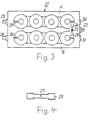
- the high frequency diplexer 21 comprises a rectangular block of conductive material in which is formed a high bandpass filter A and a low bandpass filter B.
- Each filter comprises four aperture coupled co-axial resonators of predetermined dimensions.
- the resonators are similar to those described above in relation to Figures 1 and 2.
- the diplexer 21 includes a single input port 22 comprising a conductor 23 which extends into a passage 24 connecting the first resonator of filter A to the first resonator of filter B, and two output ports 25 and 26.
- Output port 25 comprises a conductor 27 which extends into the last resonator of filter A
- output port 26 comprises a conductor 28 which extends into the last resonator of filter B.
- Conductor 23 of input port 22 is connected to a flat elongated resilient conductor 29 at a point intermediate the length of the conductor.
- the length of the conductor is such that each end thereof resiliently abuts the point of a respective adjustment screw 30 and 31, adjustment screw 30 extending into the first resonator of filter A and adjustment screw 31 extending into the first resonator of filter B.
- the shaft and point of adjustment screws 30 and 31 are mode of suitable electrical insulating material such as, for example, aluminium oxide.
- Optimum coupling of the input port to filters A and B is obtained by operating screws 30 and 31 to move the ends of conductor 29 in relation to the resonator rods of the first resonators, and using a return loss measurement means or any other known means for measuring the reflection factor to locate optimum impedance match between elements connected to the input port and filters A and B.
Landscapes
- Physics & Mathematics (AREA)
- Electromagnetism (AREA)
- Control Of Motors That Do Not Use Commutators (AREA)
Description
- Figure 1
- shows a top view of the mechanical structure of a bandpass filter incorporating the adjustable coupling arrangement of the present invention.
- Figure 2
- shows a cross-sectional view of the mechanical structure shown in Figure 1.
- Figure 3
- shows a top view of the mechanical structure of a diplexer filter incorporating the adjustable coupling arrangement of the present invention.
- Figure 4
- shows a side view of a conductive element of the coupling arrangement shown in Figure 3.
Claims (3)
- A radio frequency filter comprising a housing means containing a plurality of co-axial resonator elements (2,3,4 and 5), an input port means (15,30,31) and at least one output port means (17,25 and 26), the filter further including an arrangement for adjustably coupling the input port means to at least one resonator element (2), the arrangement comprising an elongated resilient conductor element (19) of predetermined dimensions that is arranged to couple the input port means (15,30,31) to the electric field zone of a first one of a plurality of coupled resonator elements, characterized in that the resilient conductor element (19) is arranged to capacitively couple the input port to the respective electric field zone and co-operates with lever means (20) of electrical insulating material that can be manually activated by a connected actuating means (20a) mounted externally in a wall of the housing means, to move the resilient conductive element (19) thereby adjusting capacitive coupling between the input port means (15,30,31) and the resonator element's electric field.
- A radio frequency filter as claimed in claim 1, characterised in that the housing means contains a first array of coupled resonator elements (A) and an adjoining second array of coupled resonator elements (B), the input port means (22) being common to both arrays and respective output port means (25,26) for each array.
- A radio frequency filter as claimed in claim 2, characterised in that each end portion of said resilient conductor (29) is relatively wider than the portion therebetween.
Applications Claiming Priority (3)
| Application Number | Priority Date | Filing Date | Title |
|---|---|---|---|
| AUPO0764A AUPO076496A0 (en) | 1996-07-01 | 1996-07-01 | Input coupling adjustment arrangement for radio frequency filters |
| AUPO0764/96 | 1996-07-01 | ||
| AUPO076496 | 1996-07-01 |
Publications (2)
| Publication Number | Publication Date |
|---|---|
| EP0817301A1 EP0817301A1 (en) | 1998-01-07 |
| EP0817301B1 true EP0817301B1 (en) | 2002-09-11 |
Family
ID=3795080
Family Applications (1)
| Application Number | Title | Priority Date | Filing Date |
|---|---|---|---|
| EP97110682A Expired - Lifetime EP0817301B1 (en) | 1996-07-01 | 1997-07-01 | Input coupling adjustment arrangement for radio frequency filters |
Country Status (4)
| Country | Link |
|---|---|
| EP (1) | EP0817301B1 (en) |
| AU (1) | AUPO076496A0 (en) |
| CA (1) | CA2209419C (en) |
| DE (1) | DE69715329T2 (en) |
Cited By (1)
| Publication number | Priority date | Publication date | Assignee | Title |
|---|---|---|---|---|
| WO2023159482A1 (en) | 2022-02-25 | 2023-08-31 | Telefonaktiebolaget Lm Ericsson (Publ) | A communication device |
Families Citing this family (2)
| Publication number | Priority date | Publication date | Assignee | Title |
|---|---|---|---|---|
| DE19926571A1 (en) * | 1999-06-11 | 2000-12-14 | Bosch Gmbh Robert | Microwave filter |
| KR101561285B1 (en) | 2014-03-28 | 2015-10-20 | 주식회사 이너트론 | Multi-band filter |
Family Cites Families (5)
| Publication number | Priority date | Publication date | Assignee | Title |
|---|---|---|---|---|
| GB849490A (en) * | 1957-09-24 | 1960-09-28 | Gen Electric Co Ltd | Improvements in or relating to coupling devices for coupling a coaxial transmission line to an electrical device |
| DE3028925A1 (en) * | 1980-07-30 | 1982-02-11 | Siemens AG, 1000 Berlin und 8000 München | Quarter wave branch connector for HF aerials - has junction with coupling loops at input resonators of twin parallel filters |
| FR2629276B1 (en) * | 1988-03-23 | 1991-06-07 | Alcatel Thomson Faisceaux | ADJUSTING MICROWAVE DEVICE FOR A PLANAR WAVE-LINE TRANSITION |
| DE4005230A1 (en) * | 1990-02-20 | 1991-08-22 | Bosch Gmbh Robert | UHF filter circuitry - has extra conductor, as output coupling bracket, adjacent to output circuit |
| FR2722338B1 (en) * | 1994-07-07 | 1996-09-13 | Europ Communities | COUPLING AND ADAPTING DEVICE FOR TRANSMITTING HIGH FREQUENCY OR MICROWAVE SIGNALS |
-
1996
- 1996-07-01 AU AUPO0764A patent/AUPO076496A0/en not_active Abandoned
-
1997
- 1997-06-30 CA CA002209419A patent/CA2209419C/en not_active Expired - Fee Related
- 1997-07-01 DE DE69715329T patent/DE69715329T2/en not_active Expired - Lifetime
- 1997-07-01 EP EP97110682A patent/EP0817301B1/en not_active Expired - Lifetime
Cited By (2)
| Publication number | Priority date | Publication date | Assignee | Title |
|---|---|---|---|---|
| WO2023159482A1 (en) | 2022-02-25 | 2023-08-31 | Telefonaktiebolaget Lm Ericsson (Publ) | A communication device |
| EP4437618A4 (en) * | 2022-02-25 | 2025-08-06 | Ericsson Telefon Ab L M | COMMUNICATION DEVICE |
Also Published As
| Publication number | Publication date |
|---|---|
| EP0817301A1 (en) | 1998-01-07 |
| CA2209419C (en) | 2000-08-15 |
| DE69715329D1 (en) | 2002-10-17 |
| AUPO076496A0 (en) | 1996-07-25 |
| DE69715329T2 (en) | 2003-05-22 |
| CA2209419A1 (en) | 1998-01-01 |
Similar Documents
| Publication | Publication Date | Title |
|---|---|---|
| US6025764A (en) | Input coupling adjustment arrangement for radio frequency filters | |
| US4742562A (en) | Single-block dual-passband ceramic filter useable with a transceiver | |
| US5432489A (en) | Filter with strip lines | |
| US5428325A (en) | RF filters and multiplexers with resonator decouplers | |
| AU555342B2 (en) | Ceramic bandpass filter | |
| EP1604425B1 (en) | Resonator filter | |
| US4216448A (en) | Microwave distributed-constant band-pass filter comprising projections adjacent on capacitively coupled resonator rods to open ends thereof | |
| US4477785A (en) | Generalized dielectric resonator filter | |
| EP0586760B1 (en) | Single toroid hybrid mode RF phase shifter | |
| GB2353144A (en) | Combline filter | |
| JPS61262301A (en) | Ceramic filter and wireless tranceiver using the same | |
| CN1122364C (en) | Multiple transmission bands wave filter | |
| US5065119A (en) | Narrow-band, bandstop filter | |
| JPS6353723B2 (en) | ||
| US20080100402A1 (en) | Monoblock RF resonator/filter | |
| US4644303A (en) | Multiple cavity square prism filter transmitter combiner with shared square walls and tuning controls mounted on rectangular end walls | |
| JPS6325523B2 (en) | ||
| US5418509A (en) | High frequency comb-like filter | |
| EP0466069B1 (en) | Microwave stripline resonators | |
| EP0817301A1 (en) | Input coupling adjustment arrangement for radio frequency filters | |
| AU729945B2 (en) | Input coupling adjustment arrangement for radio frequency filters | |
| US5170138A (en) | Single toroid hybrid mode RF phase shifter | |
| US6525625B1 (en) | Dielectric duplexer and communication apparatus | |
| US5105174A (en) | Wave-guide band rejection filter having a short circuited coaxial tuning screw | |
| JP2630387B2 (en) | Dielectric filter |
Legal Events
| Date | Code | Title | Description |
|---|---|---|---|
| PUAI | Public reference made under article 153(3) epc to a published international application that has entered the european phase |
Free format text: ORIGINAL CODE: 0009012 |
|
| AK | Designated contracting states |
Kind code of ref document: A1 Designated state(s): DE DK FI FR IT SE |
|
| RIN1 | Information on inventor provided before grant (corrected) |
Inventor name: TREMBATH, NATALIE Inventor name: PELZ DIETER, |
|
| 17P | Request for examination filed |
Effective date: 19980204 |
|
| AKX | Designation fees paid |
Free format text: DE DK FI FR IT SE |
|
| RBV | Designated contracting states (corrected) |
Designated state(s): DE DK FI FR IT SE |
|
| RAP3 | Party data changed (applicant data changed or rights of an application transferred) |
Owner name: ALCATEL |
|
| RAP3 | Party data changed (applicant data changed or rights of an application transferred) |
Owner name: ALCATEL |
|
| 17Q | First examination report despatched |
Effective date: 20001212 |
|
| GRAG | Despatch of communication of intention to grant |
Free format text: ORIGINAL CODE: EPIDOS AGRA |
|
| GRAG | Despatch of communication of intention to grant |
Free format text: ORIGINAL CODE: EPIDOS AGRA |
|
| GRAH | Despatch of communication of intention to grant a patent |
Free format text: ORIGINAL CODE: EPIDOS IGRA |
|
| GRAH | Despatch of communication of intention to grant a patent |
Free format text: ORIGINAL CODE: EPIDOS IGRA |
|
| GRAA | (expected) grant |
Free format text: ORIGINAL CODE: 0009210 |
|
| AK | Designated contracting states |
Kind code of ref document: B1 Designated state(s): DE DK FI FR IT SE |
|
| PG25 | Lapsed in a contracting state [announced via postgrant information from national office to epo] |
Ref country code: FI Free format text: LAPSE BECAUSE OF FAILURE TO SUBMIT A TRANSLATION OF THE DESCRIPTION OR TO PAY THE FEE WITHIN THE PRESCRIBED TIME-LIMIT Effective date: 20020911 |
|
| REF | Corresponds to: |
Ref document number: 69715329 Country of ref document: DE Date of ref document: 20021017 |
|
| PG25 | Lapsed in a contracting state [announced via postgrant information from national office to epo] |
Ref country code: SE Free format text: LAPSE BECAUSE OF FAILURE TO SUBMIT A TRANSLATION OF THE DESCRIPTION OR TO PAY THE FEE WITHIN THE PRESCRIBED TIME-LIMIT Effective date: 20021211 Ref country code: DK Free format text: LAPSE BECAUSE OF FAILURE TO SUBMIT A TRANSLATION OF THE DESCRIPTION OR TO PAY THE FEE WITHIN THE PRESCRIBED TIME-LIMIT Effective date: 20021211 |
|
| ET | Fr: translation filed | ||
| PLBE | No opposition filed within time limit |
Free format text: ORIGINAL CODE: 0009261 |
|
| STAA | Information on the status of an ep patent application or granted ep patent |
Free format text: STATUS: NO OPPOSITION FILED WITHIN TIME LIMIT |
|
| 26N | No opposition filed |
Effective date: 20030612 |
|
| REG | Reference to a national code |
Ref country code: FR Ref legal event code: GC Effective date: 20140717 |
|
| REG | Reference to a national code |
Ref country code: FR Ref legal event code: RG Effective date: 20141016 |
|
| REG | Reference to a national code |
Ref country code: FR Ref legal event code: PLFP Year of fee payment: 19 |
|
| PGFP | Annual fee paid to national office [announced via postgrant information from national office to epo] |
Ref country code: FR Payment date: 20150626 Year of fee payment: 19 |
|
| PGFP | Annual fee paid to national office [announced via postgrant information from national office to epo] |
Ref country code: DE Payment date: 20150721 Year of fee payment: 19 |
|
| PGFP | Annual fee paid to national office [announced via postgrant information from national office to epo] |
Ref country code: IT Payment date: 20150727 Year of fee payment: 19 |
|
| REG | Reference to a national code |
Ref country code: DE Ref legal event code: R119 Ref document number: 69715329 Country of ref document: DE |
|
| PG25 | Lapsed in a contracting state [announced via postgrant information from national office to epo] |
Ref country code: DE Free format text: LAPSE BECAUSE OF NON-PAYMENT OF DUE FEES Effective date: 20170201 Ref country code: FR Free format text: LAPSE BECAUSE OF NON-PAYMENT OF DUE FEES Effective date: 20160801 |
|
| REG | Reference to a national code |
Ref country code: FR Ref legal event code: ST Effective date: 20170331 |
|
| PG25 | Lapsed in a contracting state [announced via postgrant information from national office to epo] |
Ref country code: IT Free format text: LAPSE BECAUSE OF NON-PAYMENT OF DUE FEES Effective date: 20160701 |