EP0813134A2 - A circuit and method for selectively enabling clock outputs - Google Patents
A circuit and method for selectively enabling clock outputs Download PDFInfo
- Publication number
- EP0813134A2 EP0813134A2 EP97304131A EP97304131A EP0813134A2 EP 0813134 A2 EP0813134 A2 EP 0813134A2 EP 97304131 A EP97304131 A EP 97304131A EP 97304131 A EP97304131 A EP 97304131A EP 0813134 A2 EP0813134 A2 EP 0813134A2
- Authority
- EP
- European Patent Office
- Prior art keywords
- clock
- transistor
- transmission line
- coupled
- clock signal
- Prior art date
- Legal status (The legal status is an assumption and is not a legal conclusion. Google has not performed a legal analysis and makes no representation as to the accuracy of the status listed.)
- Withdrawn
Links
Images


Classifications
-
- G—PHYSICS
- G06—COMPUTING OR CALCULATING; COUNTING
- G06F—ELECTRIC DIGITAL DATA PROCESSING
- G06F1/00—Details not covered by groups G06F3/00 - G06F13/00 and G06F21/00
- G06F1/04—Generating or distributing clock signals or signals derived directly therefrom
- G06F1/10—Distribution of clock signals, e.g. skew
Definitions
- the present invention relates generally to the field of electronics. More particularly, the present invention relates to a clock circuit that selectively drives a clock signal to an option module via a transmission line when the option module is coupled to the clock circuit, and prevents propagation of the clock signal through the transmission line when the option module is decoupled from the clock circuit.
- CMOS Complementary Metal-Oxide Silicon
- each transmission line may include, but are not limited to a first segment of a printed trace line implemented on the motherboard, a second segment of a printed trace line implemented on an option module.
- the connectors coupling the first and second segments of printed trace lines influence the impedance of the transmission line.
- an option module provides enhanced functionality to the electronic system.
- each transmission line must be terminated. Such termination may be accomplished, for example, by placing a termination resistor proximate to a load receiving a system clock signal.
- the termination resistor is configured with impedance equal to that of the transmission line and is coupled to both ground and the transmission line.
- the termination resistor Since it is desirous for the termination resistor to be in close proximity to the load, the termination resistor usually is placed on the option module. Thus, when the option module is implemented within the electronic system by connecting the option module to one of the connectors, the transmission line associated with the connector is properly terminated. However, when the option module is removed from the electronic system, the transmission line associated with that option module has no termination. Hence, the transmission line radiates EMI along the transmission line creating difficulties in meeting Federal guidelines on EMI limits produced by computers and other electronic systems.
- a pair of reversed biased diodes e.g., Shottkey diode clamp
- anode of a first diode may be coupled to a supply voltage reference (e.g., a +5.0 volt "V" supply) and a cathode of a second diode may be coupled to a ground reference.
- V voltage reference
- the first and second diodes maintain the voltage parameters ranging from approximately +5.4V and approximately -0.4V for a CMOS clock driver, taking into account forward conduction voltage of the diode being equal to approximately 0.4V.
- the clock drivers are being implemented with either Emitter Coupled Logic ("ECL”) or Positive Emitter Coupled Logic ("PECL").
- ECL Emitter Coupled Logic
- PECL Positive Emitter Coupled Logic
- the conventional architecture of the clocking circuitry now has become subject to a number of disadvantages.
- One primary disadvantage is that the conventional clocking circuitry fails to eliminate propagation of a clock signal along the transmission lines when the option module is removed from the electronic system.
- the EMI radiating from the transmission lines increases. Therefore, it is more difficult to design faster electronic systems employing conventional clocking circuitry due to an increase in skew between the system clock signals.
- An embodiment of the invention can provide a clock circuit for selectively enabling a clock signal to be propagated, via a transmission line, to an option module only when the module is coupled to the clock circuit. Otherwise, when the option module is decoupled from the clock circuit, the clock signal is precluded from propagating through the transmission line(s). As a result, EMI radiation is substantially diminished.
- the clock circuit includes a clock driving element employed within a first module and a clock receiving element employed within a second module.
- the clock driving element includes a clock driver, normally an amplifier connected to at least one emitter-follower transistor.
- a pull-up resistor is coupled to the emitter of the emitter-follower transistor.
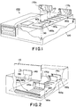
- Figure 1 is a perspective view of an embodiment of the present invention implemented within a first embodiment of an electronic system including a plurality of option modules coupled to the motherboard through a corresponding pair of connectors.
- Figure 2 is a perspective view of an embodiment of the present invention implemented within a second embodiment of an electronic system including a plurality of option modules electrically coupled to the motherboard through a corresponding pair of connectors.
- Figure 3 is a block diagram of an embodiment of a selective clock circuit including the clock driving element of Figure 1 and a pair of clock receiving elements associated with two connected option modules of the plurality of option modules.
- Figure 4 is a block diagram illustrating in greater detail the embodiment of the selective clock circuit of Figures 1-3 .
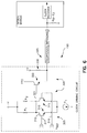
- FIG 5 is a detailed schematic diagram of a first embodiment of the clock driving element of Figure 4 including a differential clock driver.
- FIG. 6 is a detailed schematic diagram of a second embodiment of the clock driving element of Figure 4 including a single ended clock driver.
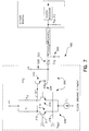
- FIG 7 is a detailed schematic of a third embodiment of the clock_ driving element of Figure 4 including a varactor diode reducing base-emitter junction capacitance.
- Figure 8 is a flowchart of an illustrative embodiment of the operational steps performed by the selective clock circuit of Figure 4 .
- An embodiment of the invention provides a selective clock circuit and its associated communication scheme which selectively enables transmission of a clock signal to an option module via transmission line(s) when implemented within an electronic system, and disables transmission of the clock signal when the option module is removed from the electronic system by deactivating the transmission line(s).
- transmission line(s) One or more transmission lines may be referred herein as "transmission line(s)".
- the electronic system 100 comprises a motherboard 110 implemented within a chassis 120 of the electronic system 100.
- the motherboard 110 comprises a clock generation element 130, a clock driving element 140, and a plurality of connectors 150 1 -150 n ("n" ⁇ 2, "n" being a whole number) as shown. It is contemplated, however, that only one connector may be used or that the connectors 150 1 -150 n may be employed as part of a backplane architecture 160 as shown in Figure 2 .
- the motherboard 110 is a removable module coupled to the backplane 160 which electrically couples other removable modules.
- each of the plurality of connectors 150 1 -l50 n is configured to receive a particular type of option module 170 1 -170 n such as, for example, a memory module, a graphics module, a processor module and the like.
- the processor module would provide multiple processor capability to the electronic system 100, while the graphics module would provide video capability.
- the memory module would provide additional memory capability.
- the clock generation element 130 includes, but is not limited to, a crystal oscillator or a phase-locked loop based circuit.
- the clock generation circuit 130 produces a master clock signal and transfer that signal to the clock driving element 140 which replicates the master clock signal forming a plurality of system clock signals.
- These system clock signals are capable of being transferred through trace lines 180 1 -180 n .
- these trace lines 180 1 -180 n are arranged in parallel and in close proximity to one another in order to reduce noise susceptibility and skew between the system clock signals.
- the clock driving element 140 includes a plurality of clock drivers (not shown) preferably processed on the same silicon die. Such processing reduces skew associated with the system clock signals produced by the clock drivers, resulting from, for example, environmental changes applied to the IC package (temperature variations, moisture, etc.) as well as voltage or current changes applied to the silicon die itself.
- the selective clock circuit 190 is illustrated as circuitry which enables transmission of system clock signals to option modules implemented within the electronic system, such as option modules 170 1 and 170 2 .
- the selective clock circuit 190 disables transmission of system clock signals when its associated option module is removed from the electronic system.
- system clock signals normally propagated along transmission lines 180 3 -180 n may be set to a voltage within a constant, predetermined voltage range such as 5V or 3.3V from PECL or ground for ECL.
- the selective clock circuit 190 includes the clock driving element 140 and a plurality of clock receiving elements 195 1 and 195 2 , which are implemented on option modules 180 1 and 180 2 .
- the clock driving element 140 includes a plurality of clock drivers (not shown) of which two clock drivers are transferring system clock signals to its uniquely dedicated clock receiving elements 195 1 and 195 2 . It is contemplated, however, that one clock driver may be configured to drive system clock signals to multiple clock receiving elements.
- the selective clock circuit 190 supporting at least one option module is shown with a clock driving element 140, including a clock driver 200, in communication with a clock receiving element 195 1 including a clock receiver 250.
- Both the clock driver 200 and the clock receiver 250 are constructed with PECL or ECL (i.e., "(P)ECL") logic and may be either "single ended” or “differential”.
- PECL or ECL i.e., "(P)ECL”
- P ECL
- P single-ended
- one communication line is used to transfer clocking signals between the clock driver 200 and the clock receiver 250.
- differential (P)ECL logic two communication lines are used to transfer clocking signals in which the clock receiver 250 observes the differences between the two communication lines.
- (P)ECL logic produces low-amplitude clocking signals (e.g., approximately 0.80V in amplitude)
- single-ended (P)ECL logic is more susceptible to signal corruption by crosstalk and other conditions than differential (P)ECL logic. Therefore, selection of ECL or PECL logic is a design choice.
- the advantage in using (P)ECL instead of TTL or CMOS logic is that (P)ECL logic outputs low-skew signals (e.g., approximately 0.05 nanoseconds "ns"), is capable of driving low-impedance transmission lines (e.g., characteristic impedances of 25 ohms " ⁇ ") and can withstand loading effects of the option modules.
- the clock driver 200 is coupled to a connector interface 255 of an option module 170 1 through a first segment 261 of transmission line(s) 260.
- the clock driver 200 receives a first reference having "V 1 " volts (e.g., normally +5V ⁇ , V 1 ⁇ 2V for PECL logic, or generally ground for ECL logic) from signal line 201 and second reference through signal line 202 (e.g., ground when using PECL logic as shown, or ranging between -2V and -5V for ECL logic).
- a pull-up resistor 203 is coupled to both the first segment 26i of transmission line(s) 260 at the output of the clock driver 200 and to a voltage source (e.g., power bus) supplying V 1 .
- the pull-up resistor 203 is configured to have a resistance "R L " substantially greater than the collective characteristic impedance of transmission line(s) 260 being equal to Z 0 (e.g., 100 ⁇ ⁇ Z 0 ⁇ 15 ⁇ ).
- the resistance "R L " of the pull-up resistor 203 may range from 1k ⁇ to 10k ⁇ , although this range is not exclusive.
- the connector interface 255 includes a male and female connection pair or any other connection mechanism.
- the connector interface 255 couples the first segment 261 of the transmission line(s) 260 to a second segment 262 of the transmission line(s) 260 used to route a system clock signal to the clock receiver 250.
- a termination circuit 265 is coupled between the second segment 262 of the transmission line(s) and ground in order to terminate the transmission line(s) 260 to reduce EMI effects therefrom.
- the termination circuit 265 is shown as a resistor 266 having a resistance "R T " equal to impedance Z 0 .
- the termination circuit 265 may include a "Thevenin" circuit or any circuit functioning in a similar manner.
- the clock driver 200 includes a dual input, differential amplifier 205 coupled to a plurality of emitter-follower transistors 215 and 220 which transfer clock information to the option module 170 1 .
- the differential amplifier 205 includes a pair of transistors 206 and 210 operating in a complementary manner.
- the pair of transistors include a first transistor 206 including a base 207, emitter 208 and collector 209 and a second transistor 210 including a base 211, emitter 212 and collector 213.
- Collectors 209 and 213 of the first and second transistors 206 and 210 are connected to bases 216 and 221 of the emitter-follower transistors 215 and 220, respectively.
- the bases 216 and 221 of the emitter-follower transistors 215 and 220 receive complementary system clock signals from the differential amplifier 205.
- the emitter-follower transistors 215 and 220 route complementary system clock signals to the option module 170 1 when the option module 170 1 is coupled to the first segment 261 of transmission line(s) 260. More specifically, the emitter-follower transistors 215 and 220 may operate as current amplifiers to provide enough current to the clock receiver 250 while still charging capacitance of the transmission line.
- the termination resistors 267 and 268 are used to reduce reflections on the transmission lines 260 as well as for DC-biasing.
- the termination resistors 267 and 268 have respective resistances "R 5 " and "R 6 " which are generally equal to the "Z 1 " and "Z 2 " impedances, respectively.
- the pull-up resistors 225 and 230 having resistances of "R 3 " and “R 4 " substantially greater than Z 1 and Z 2 , raise the voltage applied on the emitters 217 and 222 of the emitter-follower transistors 215 and 220 above the voltage applied to the bases 216 and 221, respectively. As a result, the emitter-follower transistors 215 and 220 are turned off. This reduces EMI within the electronic system employing the option module 170 1 and sensitive clock circuit 190. Otherwise, the pull-up resistors 225 and 230 have no effect.
- the clock driver 300 includes a single-input, differential amplifier 305 in which a base 311 of the first transistor 310 receives the system clock signal while a base 316 of the second transistor 315 receives a predetermined voltage ("V ref ").
- V ref is selected so that there will be positive and negative voltage differences between V ref and the voltage of the system clock signal as it oscillates.
- the collector 312 of the first transistor 310 is coupled to the base 321 of a emitter-follower transistor 320.
- the collector and emitter of the emitter-follower transistor 320 are coupled to a voltage reference "V 2 " (e.g., positive voltage for PECL logic, or generally ground for ECL logic) and the transmission line 325, respectively.
- V 2 e.g., positive voltage for PECL logic, or generally ground for ECL logic
- a pull-up resistor 330 is coupled to the transmission line 325 and the voltage reference in order to turn off the emitter-follower transistor 320 when the option module is removed (e.g., when the connection between the option module 170 1 and the transmission line(s) 325 is disconnected).
- the emitter-follower transistor 320 is turned off by raising the voltage at the emitter of the emitter-follower transistor 320 to exceed the voltage applied to its base 321. Otherwise, when the option module 170 1 is coupled to the transmission lines 325, the pull-up resistor 330 has no effect.
- a varactor diode 335 (normally paracetic in nature) is implemented at the base-emitter junction of emitter-follower transistor 320 of Figure 6 as well as the emitter-follower transistors 215 and 220 of Figure 5 .
- the pull-up resistor 330 reverse biases the base-emitter junction causing the transistor 320 to turn-off when the option module is not connected to the first segment of the transmission line(s).
- the pull-up resistor 330 biases the varactor diode in a way to reduce the capacitance (“C J ”) at the base-emitter junction.
- the voltage divider being C J /C T2 , where "C T2 " is equal to the total capacitance along the transmission line(s) 325, transfers a reduced amplitude signal to the transmission line(s) further reducing EMI.
- the communication scheme used by the selective clock circuit is shown below.
- the clock receiving element operating as a "slave” device is implemented onto each of the option modules.
- a clock driving element operating as a "master” device by providing system clock signals to the clock receiving element of the option modules coupled thereto.
- the transmission lines remain terminated.
- the pull-up resistor of the clock driving element applies the predetermined voltage to an emitter-follower transistor to turn off the transistor (Steps 405 and 410).
- the predetermined voltage deactivates the transmission lines until a coupling with the option module is re-established (Step 415).
- the emitter-follower transistor is turned on (Step 420). This process would continue repeatedly for the coupling or decoupling of option modules.
Landscapes
- Engineering & Computer Science (AREA)
- Theoretical Computer Science (AREA)
- Physics & Mathematics (AREA)
- General Engineering & Computer Science (AREA)
- General Physics & Mathematics (AREA)
- Logic Circuits (AREA)
Abstract
Description
- The present invention relates generally to the field of electronics. More particularly, the present invention relates to a clock circuit that selectively drives a clock signal to an option module via a transmission line when the option module is coupled to the clock circuit, and prevents propagation of the clock signal through the transmission line when the option module is decoupled from the clock circuit.
- It is well known that many electronic systems (e.g., computers, workstations, mainframes, etc.) are designed with a number of printed circuit boards which are electrically coupled together. One of these printed circuit boards, referred to as the "motherboard", includes a clock generation circuit (e.g., crystal oscillator) that produces a "master clock signal", being the main clock utilized by the electronic system. The master clock signal is replicated to generate a plurality of copies, which are referred to as "system clock signals". Each of the system clock signals is driven to different portions of the electronic system by a clock driver. For those outdated system architectures utilizing low-speed clock frequencies (e.g., 33 megahertz "MHz" or less), the clock drivers typically employ Transistor-Transistor logic ("TTL") or Complementary Metal-Oxide Silicon ("CMOS") logic.
- Of the plurality of system clock signals produced, a number of these system clock signals may be routed by transmission lines to removable option modules such as graphics cards, processor cards and the like. Each transmission line may include, but are not limited to a first segment of a printed trace line implemented on the motherboard, a second segment of a printed trace line implemented on an option module. Of course, the connectors coupling the first and second segments of printed trace lines influence the impedance of the transmission line. When coupled to the motherboard, an option module provides enhanced functionality to the electronic system.
- In order to preserve signal integrity of each system clock signal and mitigate the effects caused by electro-magnetic interference "EMI", each transmission line must be terminated. Such termination may be accomplished, for example, by placing a termination resistor proximate to a load receiving a system clock signal. The termination resistor is configured with impedance equal to that of the transmission line and is coupled to both ground and the transmission line.
- Since it is desirous for the termination resistor to be in close proximity to the load, the termination resistor usually is placed on the option module. Thus, when the option module is implemented within the electronic system by connecting the option module to one of the connectors, the transmission line associated with the connector is properly terminated. However, when the option module is removed from the electronic system, the transmission line associated with that option module has no termination. Hence, the transmission line radiates EMI along the transmission line creating difficulties in meeting Federal guidelines on EMI limits produced by computers and other electronic systems.
- For many years, this problem has been overcome by connecting a pair of reversed biased diodes (e.g., Shottkey diode clamp) to the transmission line in such a fashion to maintain the voltage of the system clock signal between two voltage parameters. For example, anode of a first diode may be coupled to a supply voltage reference (e.g., a +5.0 volt "V" supply) and a cathode of a second diode may be coupled to a ground reference. As a result, the first and second diodes maintain the voltage parameters ranging from approximately +5.4V and approximately -0.4V for a CMOS clock driver, taking into account forward conduction voltage of the diode being equal to approximately 0.4V.
- With advancements in the electronic systems resulting in the use of high clock frequencies (e.g., over 100 MHz), the clock drivers are being implemented with either Emitter Coupled Logic ("ECL") or Positive Emitter Coupled Logic ("PECL"). Thus, the conventional architecture of the clocking circuitry now has become subject to a number of disadvantages. One primary disadvantage is that the conventional clocking circuitry fails to eliminate propagation of a clock signal along the transmission lines when the option module is removed from the electronic system. As a result, as the clocking frequency used by the electronic system increases, the EMI radiating from the transmission lines increases. Therefore, it is more difficult to design faster electronic systems employing conventional clocking circuitry due to an increase in skew between the system clock signals. Likewise, it is more difficult to meet EMI limits imposed by Federal regulations.
- Hence, it would be advantageous to design a clock circuit which would provide a low-skew clock signal to the option module via one or more transmission lines when the option module is electrically coupled to the motherboard, and alternatively, discontinue supplying the low-skew clock signal to the connector reserved for the option module after the option card is removed therefrom by deactivating the transmission line(s).
- Particular and preferred aspects of the invention are set out in the accompanying independent and dependent claims.
- An embodiment of the invention can provide a clock circuit for selectively enabling a clock signal to be propagated, via a transmission line, to an option module only when the module is coupled to the clock circuit. Otherwise, when the option module is decoupled from the clock circuit, the clock signal is precluded from propagating through the transmission line(s). As a result, EMI radiation is substantially diminished.
- The clock circuit includes a clock driving element employed within a first module and a clock receiving element employed within a second module. The clock driving element includes a clock driver, normally an amplifier connected to at least one emitter-follower transistor. A pull-up resistor is coupled to the emitter of the emitter-follower transistor. Thus, when the option module is decoupled from the transmission line, the pull-up resistor appiies voitage sufficient to turn-off the transistor. Otherwise, the pull-up resistor has no effect on the clock circuit.
- Exemplary embodiments of the invention are described hereinafter, by way of example only, with reference to the accompanying drawings, in which:
- Figure 1 is a perspective view of an embodiment of the present invention implemented within a first embodiment of an electronic system including a plurality of option modules coupled to the motherboard through a corresponding pair of connectors.
- Figure 2 is a perspective view of an embodiment of the present invention implemented within a second embodiment of an electronic system including a plurality of option modules electrically coupled to the motherboard through a corresponding pair of connectors.
- Figure 3 is a block diagram of an embodiment of a selective clock circuit including the clock driving element of Figure 1 and a pair of clock receiving elements associated with two connected option modules of the plurality of option modules.
- Figure 4 is a block diagram illustrating in greater detail the embodiment of the selective clock circuit of Figures 1-3.
- Figure 5 is a detailed schematic diagram of a first embodiment of the clock driving element of Figure 4 including a differential clock driver.
- Figure 6 is a detailed schematic diagram of a second embodiment of the clock driving element of Figure 4 including a single ended clock driver.
- Figure 7 is a detailed schematic of a third embodiment of the clock_ driving element of Figure 4 including a varactor diode reducing base-emitter junction capacitance.
- Figure 8 is a flowchart of an illustrative embodiment of the operational steps performed by the selective clock circuit of Figure 4.
- An embodiment of the invention provides a selective clock circuit and its associated communication scheme which selectively enables transmission of a clock signal to an option module via transmission line(s) when implemented within an electronic system, and disables transmission of the clock signal when the option module is removed from the electronic system by deactivating the transmission line(s). Although specific circuitry has been set forth, it is obvious that these specific details are not required to practice the invention. Likewise, well known circuits, devices and the like may not be discussed in order to avoid obscuring the present invention.
- In the detailed description, a number of terms are used herein to describe certain characteristics or qualities. For example, circuitry employing Positive Emitter Coupled Logic ("PECL"), but capable of employing Emitter Coupled Logic ("ECL"), may be referred to as "(P)ECL logic." One or more transmission lines may be referred herein as "transmission line(s)".
- Referring to Figure 1, a simplified embodiment of an electronic system (e.g., computer, workstation, mainframe, etc.) utilizing the present invention is shown. The
electronic system 100 comprises amotherboard 110 implemented within achassis 120 of theelectronic system 100. Themotherboard 110 comprises aclock generation element 130, aclock driving element 140, and a plurality of connectors 1501-150n ("n" ≥ 2, "n" being a whole number) as shown. It is contemplated, however, that only one connector may be used or that the connectors 1501-150n may be employed as part of abackplane architecture 160 as shown in Figure 2. Thus, themotherboard 110 is a removable module coupled to thebackplane 160 which electrically couples other removable modules. - Referring still to Figures 1-2, each of the plurality of connectors 1501-l50n is configured to receive a particular type of option module 1701-170n such as, for example, a memory module, a graphics module, a processor module and the like. The processor module would provide multiple processor capability to the
electronic system 100, while the graphics module would provide video capability. The memory module would provide additional memory capability. - The
clock generation element 130 includes, but is not limited to, a crystal oscillator or a phase-locked loop based circuit. Theclock generation circuit 130 produces a master clock signal and transfer that signal to theclock driving element 140 which replicates the master clock signal forming a plurality of system clock signals. These system clock signals are capable of being transferred through trace lines 1801-180n. Preferably, these trace lines 1801-180n are arranged in parallel and in close proximity to one another in order to reduce noise susceptibility and skew between the system clock signals. - The
clock driving element 140 includes a plurality of clock drivers (not shown) preferably processed on the same silicon die. Such processing reduces skew associated with the system clock signals produced by the clock drivers, resulting from, for example, environmental changes applied to the IC package (temperature variations, moisture, etc.) as well as voltage or current changes applied to the silicon die itself. - Referring now to Figure 3, the
selective clock circuit 190 is illustrated as circuitry which enables transmission of system clock signals to option modules implemented within the electronic system, such asoption modules selective clock circuit 190 disables transmission of system clock signals when its associated option module is removed from the electronic system. For example, system clock signals normally propagated along transmission lines 1803-180n may be set to a voltage within a constant, predetermined voltage range such as 5V or 3.3V from PECL or ground for ECL. - The
selective clock circuit 190 includes theclock driving element 140 and a plurality of clock receiving elements 1951 and 1952, which are implemented on option modules 1801 and 1802. Theclock driving element 140 includes a plurality of clock drivers (not shown) of which two clock drivers are transferring system clock signals to its uniquely dedicated clock receiving elements 1951 and 1952. It is contemplated, however, that one clock driver may be configured to drive system clock signals to multiple clock receiving elements. - Referring now to Figure 4, the
selective clock circuit 190 supporting at least one option module is shown with aclock driving element 140, including aclock driver 200, in communication with a clock receiving element 1951 including aclock receiver 250. Both theclock driver 200 and theclock receiver 250 are constructed with PECL or ECL (i.e., "(P)ECL") logic and may be either "single ended" or "differential". For single-ended (P)ECL logic, one communication line is used to transfer clocking signals between theclock driver 200 and theclock receiver 250. For differential (P)ECL logic, two communication lines are used to transfer clocking signals in which theclock receiver 250 observes the differences between the two communication lines. Of course, since (P)ECL logic produces low-amplitude clocking signals (e.g., approximately 0.80V in amplitude), single-ended (P)ECL logic is more susceptible to signal corruption by crosstalk and other conditions than differential (P)ECL logic. Therefore, selection of ECL or PECL logic is a design choice. Furthermore, the advantage in using (P)ECL instead of TTL or CMOS logic is that (P)ECL logic outputs low-skew signals (e.g., approximately 0.05 nanoseconds "ns"), is capable of driving low-impedance transmission lines (e.g., characteristic impedances of 25 ohms "Ω") and can withstand loading effects of the option modules. - As shown, the
clock driver 200 is coupled to aconnector interface 255 of anoption module 1701 through afirst segment 261 of transmission line(s) 260. Theclock driver 200 receives a first reference having "V1" volts (e.g., normally +5V ≥, V1 ≥ 2V for PECL logic, or generally ground for ECL logic) fromsignal line 201 and second reference through signal line 202 (e.g., ground when using PECL logic as shown, or ranging between -2V and -5V for ECL logic). A pull-upresistor 203 is coupled to both the first segment 26i of transmission line(s) 260 at the output of theclock driver 200 and to a voltage source (e.g., power bus) supplying V1. The pull-upresistor 203 is configured to have a resistance "RL" substantially greater than the collective characteristic impedance of transmission line(s) 260 being equal to Z0 (e.g., 100Ω ≤ Z0 ≤ 15Ω). For example, the resistance "RL" of the pull-upresistor 203 may range from 1kΩ to 10kΩ, although this range is not exclusive. - The
connector interface 255 includes a male and female connection pair or any other connection mechanism. Theconnector interface 255 couples thefirst segment 261 of the transmission line(s) 260 to asecond segment 262 of the transmission line(s) 260 used to route a system clock signal to theclock receiver 250. Placed in close proximity with theclock receiver 250 to avoid a lengthy unterminated segment of the transmission lines coupling theclock receiver 250, atermination circuit 265 is coupled between thesecond segment 262 of the transmission line(s) and ground in order to terminate the transmission line(s) 260 to reduce EMI effects therefrom. Thetermination circuit 265 is shown as a resistor 266 having a resistance "RT" equal to impedance Z0. However, thetermination circuit 265 may include a "Thevenin" circuit or any circuit functioning in a similar manner. - Referring to Figure 5, a schematic diagram of the
selective clock circuit 190 is shown. Theclock driver 200 includes a dual input,differential amplifier 205 coupled to a plurality of emitter-follower transistors option module 1701. Thedifferential amplifier 205 includes a pair oftransistors first transistor 206 including abase 207,emitter 208 andcollector 209 and asecond transistor 210 including abase 211,emitter 212 andcollector 213.Collectors second transistors bases follower transistors - The
bases follower transistors differential amplifier 205. The emitter-follower transistors option module 1701 when theoption module 1701 is coupled to thefirst segment 261 of transmission line(s) 260. More specifically, the emitter-follower transistors clock receiver 250 while still charging capacitance of the transmission line. Thetermination resistors transmission lines 260 as well as for DC-biasing. Preferably, thetermination resistors - In the event that the
option module 1701 is decoupled fromfirst segment 261 oftransmission line 260, the pull-upresistors 225 and 230, having resistances of "R3" and "R4" substantially greater than Z1 and Z2, raise the voltage applied on theemitters follower transistors bases follower transistors option module 1701 andsensitive clock circuit 190. Otherwise, the pull-upresistors 225 and 230 have no effect. - Referring now to Figure 6, a detailed schematic diagram of the
selective clock circuit 190 employing a single endedclock driver 300 is shown. Theclock driver 300 includes a single-input,differential amplifier 305 in which abase 311 of thefirst transistor 310 receives the system clock signal while abase 316 of thesecond transistor 315 receives a predetermined voltage ("Vref"). Vref is selected so that there will be positive and negative voltage differences between Vref and the voltage of the system clock signal as it oscillates. - The
collector 312 of thefirst transistor 310 is coupled to thebase 321 of a emitter-follower transistor 320. The collector and emitter of the emitter-follower transistor 320 are coupled to a voltage reference "V2" (e.g., positive voltage for PECL logic, or generally ground for ECL logic) and thetransmission line 325, respectively. A pull-upresistor 330 is coupled to thetransmission line 325 and the voltage reference in order to turn off the emitter-follower transistor 320 when the option module is removed (e.g., when the connection between theoption module 1701 and the transmission line(s) 325 is disconnected). The emitter-follower transistor 320 is turned off by raising the voltage at the emitter of the emitter-follower transistor 320 to exceed the voltage applied to itsbase 321. Otherwise, when theoption module 1701 is coupled to thetransmission lines 325, the pull-upresistor 330 has no effect. - Referring to Figure 7, a more-detailed embodiment of the clock driving element of Figure 6 is shown. A varactor diode 335 (normally paracetic in nature) is implemented at the base-emitter junction of emitter-
follower transistor 320 of Figure 6 as well as the emitter-follower transistors resistor 330 reverse biases the base-emitter junction causing thetransistor 320 to turn-off when the option module is not connected to the first segment of the transmission line(s). In addition, the pull-upresistor 330 biases the varactor diode in a way to reduce the capacitance ("CJ") at the base-emitter junction. The voltage divider being CJ/CT2, where "CT2" is equal to the total capacitance along the transmission line(s) 325, transfers a reduced amplitude signal to the transmission line(s) further reducing EMI. - Referring to Figure 8, the communication scheme used by the selective clock circuit is shown below. Basically, as mentioned above, the clock receiving element, operating as a "slave" device is implemented onto each of the option modules. A clock driving element operating as a "master" device by providing system clock signals to the clock receiving element of the option modules coupled thereto. The transmission lines remain terminated. Next, upon detecting that the option module is decoupled from the clock driving element, the pull-up resistor of the clock driving element applies the predetermined voltage to an emitter-follower transistor to turn off the transistor (
Steps 405 and 410). As a result, the predetermined voltage deactivates the transmission lines until a coupling with the option module is re-established (Step 415). Then, the emitter-follower transistor is turned on (Step 420). This process would continue repeatedly for the coupling or decoupling of option modules. - To one skilled in the art, alternative embodiments of the invention will be apparent. The preferred embodiment provided is merely for illustrative purposes and should not be taken as limiting the scope of the invention. Clearly, other embodiments are conceivable such as different voltage levels for different types of products. Also, although specific combinations of features are set out in the dependent claims, combinations of features from the dependent claims with those of the independent claims other than those specifically enumerated by the claim dependencies may be made, as appropriate.
Claims (20)
- A clock circuit comprising:at least one transmission line;a clock receiving element removably coupled to said at least one transmission line, said clock receiving element being configured to receive at least one clock signal; anda clock driving element coupled to said at least one transmission line, said clock driving element being configured to propagate said at least one clock signal to said clock receiving element only when said clock receiving element is coupled to said at least one transmission line.
- The clock circuit according to claim 1, wherein the clock driving element is further configured to prevent propagation of said at least one clock signal through said at least one transmission line when said clock receiving element is decoupled from said at least one transmission line.
- The clock circuit according to claim 1, wherein the clock driving element includesa clock driver coupled to said at least one transmission line, said at least one clock driver includes at least one transistor including a base receiving a first voltage associated with said at least one clock signal and an emitter coupled to said at least one transmission line; andat least one pull-up resistor coupled between a voltage reference supplying a second voltage and said at least one transmission line, said at least one pull-up resistor applies said second voltage to said emitter of said at least one transistor to turn off said at least one transistor when said clock receiving element is decoupled from said at least one transmission line.
- The clock circuit according to claim 3, wherein said at least one pull-up resistor has a resistance substantially greater than a characteristic impedance of said at least one transmission line.
- The clock circuit according to claim 1, wherein said clock driver is implemented with Emitter Coupled Logic.
- The clock circuit according to claim 1, wherein said clock driver is implemented with Positive Emitter Coupled Logic.
- The clock circuit according to claim 3, wherein said clock driver further includes
an amplifier including a first transistor and a second transistor, said first transistor including a collector, an emitter and a base that receives said at least one clock signal, and said second transistor includes a base that receives a predetermined voltage reference, wherein said collector of said first transistor is coupled to said base of said at least one transistor. - The clock circuit according to claim 3, wherein said clock driver further includes
an amplifier including a first transistor having a base receiving a first clock signal of said at least one clock signal, and a second transistor having a base receiving a second clock signal of said predetermined voltage reference, wherein said at least one transistor includes a third transistor having a base coupled to a collector of said first transistor and an emitter coupled to a first transmission line of said at least one transmission line, and a fourth transistor having a base coupled to a collector of said second transistor and an emitter coupled to a second transmission line of said at least one transmission line. - A computer system comprising:a circuit board including a clock driving element and a first line segment coupled to said clock driving element; anda plurality of option modules capable of being coupled to said circuit board, wherein at least a first option module of said plurality of option modules includesa second line segment capable of being coupled to said first line segment forming a transmission line, anda clock receiving element coupled to said transmission line, whereinsaid clock driving element (i) propagates at least one clock signal to said clock receiving element if said first option module is coupled to said circuit board, and (ii) prevents said at least one clock signal from being propagated to said clock receiving element upon detecting that said first option module is decoupled from said circuit board.
- The computer system according to Claim 9, wherein said first module element includesa clock driver coupled to said first line segment, said clock driver includes at least one transistor including a base that receives a first voltage associated with said at least one clock signal, and an emitter coupled to said at least one transmission line; andat least one resistor coupled between a voltage reference supplying a second voltage and said at least one transmission line, said resistor applies said second voltage to said emitter of said at least one transistor to turn off said at least one transistor when said clock receiving element is decoupled from said at least one transmission line.
- The computer system according to claim 10, wherein said at least one resistor has a resistance substantially greater than a characteristic impedance of said at least one transmission line.
- The computer system according to claim 10, wherein said clock driver is implemented with Emitter Coupled Logic.
- The computer system according to claim 10, wherein said clock driver is implemented with Positive Emitter Coupled Logic.
- The computer system according to claim 12, wherein said clock driver includesan amplifier including a first transistor and a second transistor, said first transistor including a collector, an emitter and a base that receives said at least one clock signal, and said second transistor includes a base that receives a predetermined voltage reference, wherein said collector of said first transistor is coupled to said base of said at least one transistor.
- The computer system according to claim 13, wherein said clock driver includes
an amplifier including a first transistor having a base receiving a first clock signal of said at least one clock signal, and a second transistor having a base receiving a second clock signal of said predetermined voltage reference, wherein said at least one transistor includes a third transistor having a base coupled to a collector of said first transistor and an emitter coupled to a first transmission line of said at least one transmission line, and a fourth transistor having a base coupled to a collector of said second transistor and an emitter coupled to a second transmission line of said at least one transmission line. - A method for selectively transferring clock signals from a first module to a second module, the method comprising the steps of:generating a master clock signal on the first module;replicating said master clock signal into a plurality of system clock signals, wherein each of said plurality of system clock signals including a clocking frequency substantially equal to said master clock signal; andpropagating said system clock signal to the second module, provided the second module is coupled to the first module.
- The method according to claim 16 further comprising the step of:
preventing said clock signal from being propagated to the second module when said second module is decoupled from the first module. - The method according to claim 17, wherein said preventing steps includes the step of turning off a transistor associated with a clock driver by pulling a voltage of an emitter greater than a case of said transistor.
- A clock circuit for controlling propagation of clock signals to a removable option module, the clock circuit comprising:a transmission line;a pull-up resistor coupled to said transmission line; anda transistor including a base capable of receiving a clock signal, a collector, and an emitter coupled to said transmission line, wherein said transistor being turned off when the removable option module is decoupled from said transmission line by said pull-up resistor raising a voltage at said emitter greater than an amplitude voltage of said clock signal.
- The clock circuit according to claim 19, wherein said pull-up resistor has no effect on said transistor when the removable option module is coupled to said transmission line.
Applications Claiming Priority (2)
| Application Number | Priority Date | Filing Date | Title |
|---|---|---|---|
| US08/664,171 US6008682A (en) | 1996-06-14 | 1996-06-14 | Circuit and method for selectively enabling ECL type outputs |
| US664171 | 1996-06-14 |
Publications (2)
| Publication Number | Publication Date |
|---|---|
| EP0813134A2 true EP0813134A2 (en) | 1997-12-17 |
| EP0813134A3 EP0813134A3 (en) | 2004-04-14 |
Family
ID=24664873
Family Applications (1)
| Application Number | Title | Priority Date | Filing Date |
|---|---|---|---|
| EP97304131A Withdrawn EP0813134A3 (en) | 1996-06-14 | 1997-06-12 | A circuit and method for selectively enabling clock outputs |
Country Status (2)
| Country | Link |
|---|---|
| US (1) | US6008682A (en) |
| EP (1) | EP0813134A3 (en) |
Cited By (3)
| Publication number | Priority date | Publication date | Assignee | Title |
|---|---|---|---|---|
| EP1030309A1 (en) * | 1999-02-19 | 2000-08-23 | Sun Microsystems, Inc. | Computer system providing low skew clock signals to a synchronous memory unit |
| WO2001055824A3 (en) * | 2000-01-27 | 2002-03-07 | Primarion Inc | Apparatus suitable for providing synchronized clock signals to a microelectronic device |
| FR2834834A1 (en) * | 2002-01-14 | 2003-07-18 | Lg Philips Lcd Co Ltd | DATA TRANSMISSION DEVICE AND METHOD FOR CONTROLLING A LIQUID CRYSTAL DISPLAY PANEL |
Families Citing this family (11)
| Publication number | Priority date | Publication date | Assignee | Title |
|---|---|---|---|---|
| SE511827C2 (en) * | 1998-03-02 | 1999-12-06 | Ericsson Telefon Ab L M | Differential line drive |
| JP3471607B2 (en) * | 1998-04-24 | 2003-12-02 | 日本電気株式会社 | Pseudo earthing method and apparatus |
| JP3202196B2 (en) * | 1998-08-25 | 2001-08-27 | 沖電気工業株式会社 | Output circuit and input circuit |
| US6380787B1 (en) * | 1999-08-31 | 2002-04-30 | Micron Technology, Inc. | Integrated circuit and method for minimizing clock skews |
| JP4383601B2 (en) * | 1999-09-30 | 2009-12-16 | 株式会社東芝 | High speed memory device, socket mounting structure of high speed memory device, and method of mounting high speed memory device |
| US6271704B1 (en) * | 1999-12-14 | 2001-08-07 | Intel Corporation | Method and apparatus for balancing current in a system with two sets of termination devices |
| US6593793B1 (en) * | 2002-01-11 | 2003-07-15 | Intel Corporation | Electronic package with integrated clock distribution structure |
| US6925616B2 (en) * | 2002-10-04 | 2005-08-02 | Sun Microsystems, Inc. | Method to test power distribution system |
| KR100555673B1 (en) * | 2004-01-20 | 2006-03-03 | 삼성전자주식회사 | Option Module and Option Module Recognition Device Using Clock Frequency |
| US7119600B2 (en) * | 2004-04-20 | 2006-10-10 | Taiwan Semiconductor Manufacturing Co., Ltd. | Wide common mode high-speed differential receiver using thin and thick gate oxide MOSFETS in deep-submicron technology |
| US20130043924A1 (en) * | 2011-08-16 | 2013-02-21 | The Aerospace Corporation | Systems, Methods, and Apparatus for High-Speed Signal Buffer Circuitry |
Family Cites Families (13)
| Publication number | Priority date | Publication date | Assignee | Title |
|---|---|---|---|---|
| GB2193066B (en) * | 1986-07-07 | 1990-07-04 | Perkin Elmer Corp | Computer bus |
| US4888501A (en) * | 1988-10-19 | 1989-12-19 | Ncr Corporation | ECL to CMOS converter |
| US4912341A (en) * | 1989-04-17 | 1990-03-27 | Advanced Micro Devices, Inc. | TTL buffer circuit with active turn-off |
| US5109493A (en) * | 1989-06-30 | 1992-04-28 | Poget Computer Corp. | Structure and method for tying down an unused multi-user bus |
| JP2622612B2 (en) * | 1989-11-14 | 1997-06-18 | 三菱電機株式会社 | Integrated circuit |
| GB9001010D0 (en) * | 1990-01-17 | 1990-03-14 | Questech Ltd | Switching of emitter coupled logic data signals |
| US5164619A (en) * | 1990-11-21 | 1992-11-17 | Hewlett-Packard Company | Low skew clocking system for VLSI integrated circuits |
| JPH04268819A (en) * | 1991-02-22 | 1992-09-24 | Nec Ic Microcomput Syst Ltd | Ecl integrated circuit device |
| US5515005A (en) * | 1993-07-27 | 1996-05-07 | Murata Manufacturing Co., Ltd. | Operational amplifier |
| JPH07106851A (en) * | 1993-10-06 | 1995-04-21 | Tokai Rika Co Ltd | Oscillation circuit |
| US5469554A (en) * | 1994-06-14 | 1995-11-21 | Compaq Computer Corp. | Detecting the presence of a device on a computer system bus by altering the bus termination |
| US5581201A (en) * | 1994-06-30 | 1996-12-03 | Tandem Computers Incorporated | Apparatus for unit control and presence detection |
| US5508665A (en) * | 1994-10-31 | 1996-04-16 | Motorola, Inc. | Oscillator operable in a high impedance mode |
-
1996
- 1996-06-14 US US08/664,171 patent/US6008682A/en not_active Expired - Lifetime
-
1997
- 1997-06-12 EP EP97304131A patent/EP0813134A3/en not_active Withdrawn
Cited By (8)
| Publication number | Priority date | Publication date | Assignee | Title |
|---|---|---|---|---|
| EP1030309A1 (en) * | 1999-02-19 | 2000-08-23 | Sun Microsystems, Inc. | Computer system providing low skew clock signals to a synchronous memory unit |
| US6338144B2 (en) | 1999-02-19 | 2002-01-08 | Sun Microsystems, Inc. | Computer system providing low skew clock signals to a synchronous memory unit |
| US6640309B2 (en) | 1999-02-19 | 2003-10-28 | Sun Microsystems, Inc. | Computer system providing low skew clock signals to a synchronous memory unit |
| WO2001055824A3 (en) * | 2000-01-27 | 2002-03-07 | Primarion Inc | Apparatus suitable for providing synchronized clock signals to a microelectronic device |
| US6857081B2 (en) | 2000-01-27 | 2005-02-15 | Primarion, Inc. | Apparatus suitable for providing synchronized clock signals to a microelectronic device |
| FR2834834A1 (en) * | 2002-01-14 | 2003-07-18 | Lg Philips Lcd Co Ltd | DATA TRANSMISSION DEVICE AND METHOD FOR CONTROLLING A LIQUID CRYSTAL DISPLAY PANEL |
| US7133014B2 (en) | 2002-01-14 | 2006-11-07 | Lg. Philips Lcd Co., Ltd. | Apparatus and method for data transmission |
| CN1312652C (en) * | 2002-01-14 | 2007-04-25 | Lg.飞利浦Lcd有限公司 | Data transmission device and method |
Also Published As
| Publication number | Publication date |
|---|---|
| US6008682A (en) | 1999-12-28 |
| EP0813134A3 (en) | 2004-04-14 |
Similar Documents
| Publication | Publication Date | Title |
|---|---|---|
| US6008682A (en) | Circuit and method for selectively enabling ECL type outputs | |
| US5122691A (en) | Integrated backplane interconnection architecture | |
| US6081430A (en) | High-speed backplane | |
| JPH05235964A (en) | High-performance bus system transceiver for bus and driver for digital device | |
| US5570037A (en) | Switchable differential terminator | |
| EP1141841A1 (en) | Hot-swappable high speed point-to-point interface | |
| US6593768B1 (en) | Dual termination serial data bus with pull-up current source | |
| US6992541B2 (en) | Single to differential interfacing | |
| EP0402055A2 (en) | Method and apparatus for a rapid interconnection to a computer bus | |
| US5982192A (en) | High speed bus circuit system | |
| US7840194B2 (en) | Transmitting circuit, receiving circuit, interface switching module and interface switching method for SATA and SAS interfaces | |
| US6828819B2 (en) | High-speed memory system | |
| US5455523A (en) | Method and apparatus for non-linear transmission line termination | |
| US6483345B1 (en) | High speed level shift circuit for low voltage output | |
| US20020005734A1 (en) | Method and apparatus for programmable active termination of input/output devices | |
| EP1014584B1 (en) | Data transmitter | |
| US6744810B1 (en) | Signal repeater for voltage intolerant components used in a serial data line | |
| US4445048A (en) | High speed ribbon cable bus | |
| US5142168A (en) | Emitter-coupled logic balanced signal transmission circuit | |
| JP3181710B2 (en) | Multilayer printed circuit board module and multilayer printed circuit board device | |
| US6070206A (en) | Method and apparatus for terminating a bus | |
| US6167321A (en) | Interface module with protection circuit and method of protecting an interface | |
| JP3989628B2 (en) | Data transmission / reception circuit | |
| US6646982B1 (en) | Redundant source synchronous busses | |
| JPH0785562B2 (en) | Failure detection method between communication devices |
Legal Events
| Date | Code | Title | Description |
|---|---|---|---|
| PUAI | Public reference made under article 153(3) epc to a published international application that has entered the european phase |
Free format text: ORIGINAL CODE: 0009012 |
|
| AK | Designated contracting states |
Kind code of ref document: A2 Designated state(s): AT BE CH DE DK ES FI FR GB GR IE IT LI LU MC NL PT SE |
|
| RAP1 | Party data changed (applicant data changed or rights of an application transferred) |
Owner name: SUN MICROSYSTEMS, INC. |
|
| PUAL | Search report despatched |
Free format text: ORIGINAL CODE: 0009013 |
|
| AK | Designated contracting states |
Kind code of ref document: A3 Designated state(s): AT BE CH DE DK ES FI FR GB GR IE IT LI LU MC NL PT SE |
|
| 17P | Request for examination filed |
Effective date: 20040930 |
|
| AKX | Designation fees paid |
Designated state(s): GB |
|
| 17Q | First examination report despatched |
Effective date: 20041228 |
|
| REG | Reference to a national code |
Ref country code: DE Ref legal event code: 8566 |
|
| STAA | Information on the status of an ep patent application or granted ep patent |
Free format text: STATUS: THE APPLICATION IS DEEMED TO BE WITHDRAWN |
|
| 18D | Application deemed to be withdrawn |
Effective date: 20080228 |