EP0809394A2 - Active pixel sensor with switched supply row select - Google Patents
Active pixel sensor with switched supply row select Download PDFInfo
- Publication number
- EP0809394A2 EP0809394A2 EP97201415A EP97201415A EP0809394A2 EP 0809394 A2 EP0809394 A2 EP 0809394A2 EP 97201415 A EP97201415 A EP 97201415A EP 97201415 A EP97201415 A EP 97201415A EP 0809394 A2 EP0809394 A2 EP 0809394A2
- Authority
- EP
- European Patent Office
- Prior art keywords
- pixel
- active pixel
- amplifier
- row select
- transistor
- Prior art date
- Legal status (The legal status is an assumption and is not a legal conclusion. Google has not performed a legal analysis and makes no representation as to the accuracy of the status listed.)
- Granted
Links
- 238000000034 method Methods 0.000 claims abstract description 15
- 238000009792 diffusion process Methods 0.000 description 8
- 230000035945 sensitivity Effects 0.000 description 8
- 238000012546 transfer Methods 0.000 description 6
- 230000008901 benefit Effects 0.000 description 4
- 238000010586 diagram Methods 0.000 description 4
- 239000007787 solid Substances 0.000 description 4
- 230000005540 biological transmission Effects 0.000 description 3
- 238000013459 approach Methods 0.000 description 2
- 230000008859 change Effects 0.000 description 2
- 230000000694 effects Effects 0.000 description 2
- 230000006872 improvement Effects 0.000 description 2
- 230000008569 process Effects 0.000 description 2
- 238000006243 chemical reaction Methods 0.000 description 1
- 238000003384 imaging method Methods 0.000 description 1
- 230000003116 impacting effect Effects 0.000 description 1
- 238000010348 incorporation Methods 0.000 description 1
- 238000012986 modification Methods 0.000 description 1
- 230000004048 modification Effects 0.000 description 1
- 238000012545 processing Methods 0.000 description 1
- 238000012552 review Methods 0.000 description 1
- 239000004065 semiconductor Substances 0.000 description 1
Images


Classifications
-
- H—ELECTRICITY
- H04—ELECTRIC COMMUNICATION TECHNIQUE
- H04N—PICTORIAL COMMUNICATION, e.g. TELEVISION
- H04N3/00—Scanning details of television systems; Combination thereof with generation of supply voltages
- H04N3/10—Scanning details of television systems; Combination thereof with generation of supply voltages by means not exclusively optical-mechanical
- H04N3/14—Scanning details of television systems; Combination thereof with generation of supply voltages by means not exclusively optical-mechanical by means of electrically scanned solid-state devices
- H04N3/15—Scanning details of television systems; Combination thereof with generation of supply voltages by means not exclusively optical-mechanical by means of electrically scanned solid-state devices for picture signal generation
- H04N3/155—Control of the image-sensor operation, e.g. image processing within the image-sensor
-
- H—ELECTRICITY
- H04—ELECTRIC COMMUNICATION TECHNIQUE
- H04N—PICTORIAL COMMUNICATION, e.g. TELEVISION
- H04N25/00—Circuitry of solid-state image sensors [SSIS]; Control thereof
- H04N25/70—SSIS architectures; Circuits associated therewith
- H04N25/76—Addressed sensors, e.g. MOS or CMOS sensors
- H04N25/766—Addressed sensors, e.g. MOS or CMOS sensors comprising control or output lines used for a plurality of functions, e.g. for pixel output, driving, reset or power
-
- H—ELECTRICITY
- H04—ELECTRIC COMMUNICATION TECHNIQUE
- H04N—PICTORIAL COMMUNICATION, e.g. TELEVISION
- H04N25/00—Circuitry of solid-state image sensors [SSIS]; Control thereof
- H04N25/40—Extracting pixel data from image sensors by controlling scanning circuits, e.g. by modifying the number of pixels sampled or to be sampled
Definitions
- This invention relates to the field of solid state photo-sensors, and more specifically to imagers referred to as active pixel sensors (APS).
- APS active pixel sensors
- APS are solid state imagers where each pixel contains a photo-sensing means, reset means, charge to voltage conversion means, and all or part of an amplifier.
- APS devices have been operated in a manner where each line or row of the imager is selected and then read out using a column select signal (analogous to a word and bit line in memory devices respectively).
- the row select operation has been accomplished in prior art devices by incorporation of a row select transistor in each pixel that is turned on to make that row active (see FIG. 1). Since this transistor is placed in each pixel, its inclusion reduces the fill factor for the pixel because it takes up area that could otherwise be used for the photodetector, or charge storage region. This reduces the sensitivity and saturation signal of the sensor.
- CMOS complementary metal-oxide-semiconductor
- CMOS complementary metal-oxide-semiconductor
- APS devices have the advantages of single 5V supply operation, lower power consumption, x-y addressability, image windowing, and the ability to effectively integrate signal processing electronics on-chip, when compared to CCD sensors.
- One approach to providing an image sensor with the sensitivity of a CCD and the advantages of an APS device, is to improve the fill factor and sensitivity of an APS device.
- This present invention addresses these problems that exist within the prior art by simplifying the circuitry used in addressing the imager.
- the present invention relates to the field of solid state photo-sensors and imagers, specifically imagers referred to as active pixel sensors (APS). It consists of a new method of row selection that eliminates the need for a separate row select transistor or gate per pixel, by eliminating the need for a separate row select buss in one case, and eliminating the need for a row select transistor in another case, while maintaining the ability to selectively address rows of the APS device.
- APS active pixel sensors
- a method of generating row select signals for active pixel sensors comprising the steps of: providing an active pixel sensor having a plurality of pixels arranged in columns and rows; and selecting rows within the active pixel sensor by application of a supply voltage to the supply of the in pixel amplifiers within a predetermined row to be selected and removal of the supply voltage from the supply of the in-pixel amplifiers of unselected rows.
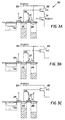
- FIG. 1 A prior art APS pixel is shown in FIG. 1.
- the pixel comprises a photodetector (PDET), that can be either a photodiode (PD) or photogate (PG), transfer gate (TG), floating diffusion (FD), reset transistor (RES), with a reset gate (RG), row select transistor (ROWST), with a row select gate (RSG), and signal transistor (SIG).
- PDET photodetector
- PG photogate
- TG transfer gate
- FD floating diffusion
- RE reset transistor
- RG reset gate
- ROWST row select transistor
- RSG row select gate
- SIG signal transistor
- This signal is read out by selecting the desired row (turning on the desired ROWST) by application of an "on-voltage" to the gate of ROWST), and then selecting each column separately. All other rows are “turned-off” by applying the appropriate signal to the gate of ROWST for those rows.
- the signal present on that line will be determined by which row is selected (i.e. the row in which ROWST is turned on).
- a simplified schematic of a single column is provided in FIG. 2. The output voltage V o , is determined by which row transistor is turned-on, since all other signal transistors are essentially disconnected.
- This invention provides a means for reducing the components required for row selection.
- the first architecture the separate row select buss is eliminated.
- row selection is accomplished without using a row select transistor per pixel.
- Two physical embodiments of the new pixel architectures are shown in Figs. 3A and 3B. Other specific physical embodiments are realizable. These two are chosen for illustration.
- the pixel comprises a PD, TG, FD, RES, RG, SIG, ROWST and row select signal line (ROWSIG). It does not contain a separate row select gate or buss (RSG).
- RSG row select gate or buss
- row selection is accomplished by applying the supply voltage VDD to the desired ROWSIG while applying OV to the remaining ROWSIG's.
- FIG. 4 A simplified schematic of one column is provided in FIG. 4. The output voltage is determined by which ROWSIG that VDD is applied to, similar to prior art except that only one buss per row is used to accomplish row select, ROWSIG, rather than 2 busses, VDD and RSG. The area that was previously used for RSG can now be used for the PD, thus improving the fill factor and sensitivity of the pixel.
- the pixel in FIG. 3B comprises a PD, TG, FD, RES, RG SIG and row select signal line (ROWSIG). It does not contain a separate row select transistor or buss (ROWST and RSG). In this architecture, row selection is accomplished by applying the supply voltage VDD to the desired ROWSIG while floating the remaining ROWSIG's.
- a simplified schematic of one column is provided in FIG. 5. The output voltage is determined by which ROWSIG that VDD is applied to, similar to prior art except that only one row select switch per row is used rather than one per pixel. The area that was previously used for ROWST cannot be used for the PD, thus improving the fill factor and sensitivity of the pixel.
- the present invention provides an advantage in that it uses less semiconductor area for control circuitry allowing more area for photodetector, thereby improving the fill factor.
- This invention relates to the field of solid state photo-sensors and imagers, specifically imagers referred to as active pixel sensors (APS). It consists of a new method of row selection that eliminates the need for a separate row select transistor or gate per pixel.
- FIG. 1 A prior APS pixel is shown in FIG. 1.
- the pixel 10 comprises a photodetector 12, that can conventionally be either a photodiode or photogate, a transfer gate 14, floating diffusion 16, reset transistor 17, with a reset gate 19, adjacent to reset drain 18, row select transistor 21, with a row select gate 23, and signal transistor 25. In this case there are 3 transistors and 4 buss lines per pixel. Pixels are arranged in an array (X-columns and Y-rows), to form an image sensor. Electrons generated in the photodetector 12 are transferred onto the floating diffusion 16 which is connected to the gate 26 of signal transistor 25.
- This signal is read out by selecting the desired row (turning on the row select transistor 21 by application of an "on-voltage" to the row select gate 26), and then selecting each column. All other rows are “turned-off” by applying the appropriate signal to the row select gate 26 for those rows. Hence when selecting a specific column (the details of this operation are not relevant to this invention), the signal present on that line will be determined by which row select transistor 21 is turned on.
- FIG. 2 A simplified schematic of a single column is provided in FIG. 2.
- the circuit configuration is a source follower with selectable signal transistors in parallel and one load transistor per column.
- the output voltage is modulated in the following manner. From Kirchoff's Current Law, the current I must be equal to I'. I' is determined by the source to gate voltage (V gs ) of the load transistor. As V in changes, I will want to change since V gs of the signal transistor changes. In order for I to remain equal to I', V gs must remain constant, hence V s of the signal transistor, which is V o , must change accordingly. With ROWST 2 turned on and all others turned off, the current I is simply I 2 since all other currents are zero because those paths to VDD are effectively open circuited by the respective ROWST's being turned off.
- the present invention provides a means for selectively connecting the desired row to the output node, and disconnecting all others, without using a separate row select buss in the first case, and in the second case, without using a row select transistor per pixel.
- Physical embodiments of the new pixel architectures are shown in Figs. 3A, 3B and 3C while other specific physical embodiments are realizable, those illustrated in FIG. 3A and 3B represent preferred embodiments of the present invention.
- pixel 30 comprises a photodetector (PD) 22, transfer gate (TG) 24, floating diffusion (FD) 26, reset transistor (RS) 27 comprising reset gate (RG) 29 and reset drain (RD) 28, the row select transistor (ROWST) 31, signal transistor (SIG) 35 and row select signal line (ROWSIG) 33. It does not contain a separate row select buss as does the prior art device illustrated in FIG. 1. It requires only 3 buss lines per pixel, those for TG 24, RG 29, ROWSIG 33, as compared to 4 busses for the prior art pixel.
- row selection is accomplished by applying the supply voltage VDD to the desired ROWSIG 33, and applying OV or the appropriate "off-signal", to the remaining ROWSIG's.
- a simplified schematic of one column is provided in FIG. 4.
- the circuit configuration is the same as in the prior art, hence the modulation of Vo occurs similarly, except that the selective connect and disconnect is done by switching the supply voltage VDD to the drain of the signal transistor and the gate of the row select transistor, rather than having a separate row select gate buss.
- this new architecture there is only one buss per row used to accomplish row select, ROWSIG, rather than 2 busses, VDD and RSG. The area that was previously used for RSG can now be used for the PD, thus improving the fill factor and sensitivity of the pixel.
- the pixel in FIG. 3B comprises a photodetector (PD) 22, transfer gate (TG) 24, floating diffusion (FD) 26, reset transistor 27 comprising reset gate 29 and reset drain 28, signal transistor (SIG) 45 and row select signal line (ROWSIG) 33. It does not contain a separate row select transistor (ROWST) 31 or row select bus (RSG) 23. It requires only 2 transistors and 3 buss lines per pixel.
- row selection is accomplished by applying, or connecting, the supply voltage VDD to the desired ROWSIG 33 while floating, or disconnecting, the remaining ROWSIG's.
- a simplified schematic of one column is provided in FIG. 5.
- the circuit configuration is similar to prior art devices, hence the modulation of Vo occurs similarly, except that the selective connect and disconnect is done by switching the supply voltage VDD to the drain of the signal transistor 45, rather than by switching a separate transistor that is in series with each signal transistor 45.
- the area that was previously used for ROWST 31 (for the embodiment shown in FIG. 3A) can now be used for the PD 22, thus improving the fill factor and sensitivity of the pixel. Also, the same fill factor could be maintained while reducing the size of the pixel and the APS device.
- the architecture of FIG. 3B provides an improvement in noise performance for three reasons.
- any noise that is present on the gate of the ROWST 21 in FIG. l will be highly capacitively coupled to the signal line (since this is the gate of a transistor), producing a noise component in the signal.
- the row select line is the VDD buss, and there is no other transistor gate coupled to the signal transistor 45.
- the SIG 45 can now be enlarged to take up some of the space previously allocated to ROWST 31. This will reduce the l/f noise of the signal transistor. Additionally, pattern noise due to non-uniform voltage drop across ROWST 31 is eliminated, since this transistor is no longer present.
- FIG. 6A is a diagram showing row select switches 60 external to the array of pixels.
- FIG. 6B is a CMOS transmission gate used as the row select switch 60.
- One method of producing this switch is by use of a CMOS transmission gate as shown in figures 6A and 6B. Since, as shown in Fig. 6A, there is only one of these row select switches 60 per row of the imager, and these are physically placed outside of the imaging array, its physical size is only limited in one dimension (i.e. it must be equal to or less than the pixel pitch), so it can be made large to reduce on-resistance without impacting fill factor of the pixel.
- FIG. 3C A variation of this architecture can be seen in Fig 3C.
- the reset drain and source follower drain are separated, so that the reset transistor supply voltage can be controlled separately from the source follower supply voltage to effect antiblooming control.
- the fill factor of this pixel architecture is improved by combining the reset gate signal and reset supply bus. This approach can also be utilized with the pixel architecture shown in FIG. 3A.
Abstract
Description
- This invention relates to the field of solid state photo-sensors, and more specifically to imagers referred to as active pixel sensors (APS).
- APS are solid state imagers where each pixel contains a photo-sensing means, reset means, charge to voltage conversion means, and all or part of an amplifier. APS devices have been operated in a manner where each line or row of the imager is selected and then read out using a column select signal (analogous to a word and bit line in memory devices respectively). The row select operation has been accomplished in prior art devices by incorporation of a row select transistor in each pixel that is turned on to make that row active (see FIG. 1). Since this transistor is placed in each pixel, its inclusion reduces the fill factor for the pixel because it takes up area that could otherwise be used for the photodetector, or charge storage region. This reduces the sensitivity and saturation signal of the sensor.
- In order to build high resolution, small pixel APS devices, it is necessary to use sub-micron CMOS processes in order to minimize the area of the pixel allocated to the row select transistor and other parts of the amplifier in the pixel. In essence, it takes a more technologically advanced and more costly process to realize the same resolution and sensitivity APS device compared to a standard charge coupled device (CCD) sensor. However, APS devices have the advantages of single 5V supply operation, lower power consumption, x-y addressability, image windowing, and the ability to effectively integrate signal processing electronics on-chip, when compared to CCD sensors.
- One approach to providing an image sensor with the sensitivity of a CCD and the advantages of an APS device, is to improve the fill factor and sensitivity of an APS device. This present invention addresses these problems that exist within the prior art by simplifying the circuitry used in addressing the imager.
- The present invention relates to the field of solid state photo-sensors and imagers, specifically imagers referred to as active pixel sensors (APS). It consists of a new method of row selection that eliminates the need for a separate row select transistor or gate per pixel, by eliminating the need for a separate row select buss in one case, and eliminating the need for a row select transistor in another case, while maintaining the ability to selectively address rows of the APS device. By employing a method of generating row select signals for active pixel sensors comprising the steps of: providing an active pixel sensor having a plurality of pixels arranged in columns and rows; and selecting rows within the active pixel sensor by application of a supply voltage to the supply of the in pixel amplifiers within a predetermined row to be selected and removal of the supply voltage from the supply of the in-pixel amplifiers of unselected rows.
- A prior art APS pixel is shown in FIG. 1. The pixel comprises a photodetector (PDET), that can be either a photodiode (PD) or photogate (PG), transfer gate (TG), floating diffusion (FD), reset transistor (RES), with a reset gate (RG), row select transistor (ROWST), with a row select gate (RSG), and signal transistor (SIG). Pixels are arranged in an array (X-columns and Y-rows), to form an image sensor. Incident light creates electrons in the photodetector. These electrons are transferred onto the floating diffusion which is connected to the gate of SIG. This signal is read out by selecting the desired row (turning on the desired ROWST) by application of an "on-voltage" to the gate of ROWST), and then selecting each column separately. All other rows are "turned-off" by applying the appropriate signal to the gate of ROWST for those rows. Hence when selecting a specific column (the details of this operation are not relevant to this invention), the signal present on that line will be determined by which row is selected (i.e. the row in which ROWST is turned on). A simplified schematic of a single column is provided in FIG. 2. The output voltage Vo, is determined by which row transistor is turned-on, since all other signal transistors are essentially disconnected.
- This invention provides a means for reducing the components required for row selection. In the first architecture, the separate row select buss is eliminated. In the second architecture, row selection is accomplished without using a row select transistor per pixel. Two physical embodiments of the new pixel architectures are shown in Figs. 3A and 3B. Other specific physical embodiments are realizable. These two are chosen for illustration.
- In the first architecture (shown in FIG. 3a), the pixel comprises a PD, TG, FD, RES, RG, SIG, ROWST and row select signal line (ROWSIG). It does not contain a separate row select gate or buss (RSG). In this architecture, row selection is accomplished by applying the supply voltage VDD to the desired ROWSIG while applying OV to the remaining ROWSIG's. A simplified schematic of one column is provided in FIG. 4. The output voltage is determined by which ROWSIG that VDD is applied to, similar to prior art except that only one buss per row is used to accomplish row select, ROWSIG, rather than 2 busses, VDD and RSG. The area that was previously used for RSG can now be used for the PD, thus improving the fill factor and sensitivity of the pixel.
- The pixel in FIG. 3B comprises a PD, TG, FD, RES, RG SIG and row select signal line (ROWSIG). It does not contain a separate row select transistor or buss (ROWST and RSG). In this architecture, row selection is accomplished by applying the supply voltage VDD to the desired ROWSIG while floating the remaining ROWSIG's. A simplified schematic of one column is provided in FIG. 5. The output voltage is determined by which ROWSIG that VDD is applied to, similar to prior art except that only one row select switch per row is used rather than one per pixel. The area that was previously used for ROWST cannot be used for the PD, thus improving the fill factor and sensitivity of the pixel.
- These and other aspects, objects, features and advantages of the present invention will be more clearly understood and appreciated from a review of the following detailed description of the preferred embodiments and appended claims, and by reference to the accompanying drawings.
- The present invention provides an advantage in that it uses less semiconductor area for control circuitry allowing more area for photodetector, thereby improving the fill factor.
-
- FIG. 1 is a diagram of a prior art pixel for an active pixel sensor;
- FIG. 2 is a simplified schematic of a single column of the active pixel sensor shown in FIG. 1;
- FIG. 3A is a diagram illustrating the active pixel sensor of the invention;
- FIG. 3B is another architecture of the active pixel sensor of the present invention;
- FIG. 3C is another architecture of the active pixel sensor of the present invention.
- FIG. 4 is a simplified column schematic for FIG. 3A; and
- FIG. 5 is a simplified column schematic for FIG. 3B.
- FIG. 6A is a diagram showing row select switches external to the array of pixels.
- FIG. 6B is a CMOS transmission gate used as the row select switch.
- To facilitate understanding, identical reference numerals have been used, where possible, to designate identical elements that are common to the figures.
- This invention relates to the field of solid state photo-sensors and imagers, specifically imagers referred to as active pixel sensors (APS). It consists of a new method of row selection that eliminates the need for a separate row select transistor or gate per pixel.
- A prior APS pixel is shown in FIG. 1. The
pixel 10 comprises aphotodetector 12, that can conventionally be either a photodiode or photogate, atransfer gate 14, floatingdiffusion 16, resettransistor 17, with areset gate 19, adjacent to resetdrain 18, rowselect transistor 21, with a rowselect gate 23, andsignal transistor 25. In this case there are 3 transistors and 4 buss lines per pixel. Pixels are arranged in an array (X-columns and Y-rows), to form an image sensor. Electrons generated in thephotodetector 12 are transferred onto the floatingdiffusion 16 which is connected to thegate 26 ofsignal transistor 25. This signal is read out by selecting the desired row (turning on the rowselect transistor 21 by application of an "on-voltage" to the row select gate 26), and then selecting each column. All other rows are "turned-off" by applying the appropriate signal to the rowselect gate 26 for those rows. Hence when selecting a specific column (the details of this operation are not relevant to this invention), the signal present on that line will be determined by which rowselect transistor 21 is turned on. - A simplified schematic of a single column is provided in FIG. 2. The circuit configuration is a source follower with selectable signal transistors in parallel and one load transistor per column. In this circuit the output voltage is modulated in the following manner. From Kirchoff's Current Law, the current I must be equal to I'. I' is determined by the source to gate voltage (Vgs) of the load transistor. As Vin changes, I will want to change since Vgs of the signal transistor changes. In order for I to remain equal to I', Vgs must remain constant, hence Vs of the signal transistor, which is Vo, must change accordingly. With ROWST2 turned on and all others turned off, the current I is simply I2 since all other currents are zero because those paths to VDD are effectively open circuited by the respective ROWST's being turned off.
- The present invention provides a means for selectively connecting the desired row to the output node, and disconnecting all others, without using a separate row select buss in the first case, and in the second case, without using a row select transistor per pixel. Physical embodiments of the new pixel architectures are shown in Figs. 3A, 3B and 3C while other specific physical embodiments are realizable, those illustrated in FIG. 3A and 3B represent preferred embodiments of the present invention.
- Referring to FIG. 3A,
pixel 30 comprises a photodetector (PD) 22, transfer gate (TG) 24, floating diffusion (FD) 26, reset transistor (RS) 27 comprising reset gate (RG) 29 and reset drain (RD) 28, the row select transistor (ROWST) 31, signal transistor (SIG) 35 and row select signal line (ROWSIG) 33. It does not contain a separate row select buss as does the prior art device illustrated in FIG. 1. It requires only 3 buss lines per pixel, those forTG 24,RG 29,ROWSIG 33, as compared to 4 busses for the prior art pixel. - In the pixel architecture of the present invention, row selection is accomplished by applying the supply voltage VDD to the desired
ROWSIG 33, and applying OV or the appropriate "off-signal", to the remaining ROWSIG's. A simplified schematic of one column is provided in FIG. 4. The circuit configuration is the same as in the prior art, hence the modulation of Vo occurs similarly, except that the selective connect and disconnect is done by switching the supply voltage VDD to the drain of the signal transistor and the gate of the row select transistor, rather than having a separate row select gate buss. With this new architecture there is only one buss per row used to accomplish row select, ROWSIG, rather than 2 busses, VDD and RSG. The area that was previously used for RSG can now be used for the PD, thus improving the fill factor and sensitivity of the pixel. - The pixel in FIG. 3B comprises a photodetector (PD) 22, transfer gate (TG) 24, floating diffusion (FD) 26, reset
transistor 27 comprisingreset gate 29 and resetdrain 28, signal transistor (SIG) 45 and row select signal line (ROWSIG) 33. It does not contain a separate row select transistor (ROWST) 31 or row select bus (RSG) 23. It requires only 2 transistors and 3 buss lines per pixel. - In this architecture, row selection is accomplished by applying, or connecting, the supply voltage VDD to the desired
ROWSIG 33 while floating, or disconnecting, the remaining ROWSIG's. A simplified schematic of one column is provided in FIG. 5. The circuit configuration is similar to prior art devices, hence the modulation of Vo occurs similarly, except that the selective connect and disconnect is done by switching the supply voltage VDD to the drain of thesignal transistor 45, rather than by switching a separate transistor that is in series with eachsignal transistor 45. With this new architecture, the area that was previously used for ROWST 31 (for the embodiment shown in FIG. 3A) can now be used for thePD 22, thus improving the fill factor and sensitivity of the pixel. Also, the same fill factor could be maintained while reducing the size of the pixel and the APS device. - In addition to the improvement in fill factor or device size, the architecture of FIG. 3B provides an improvement in noise performance for three reasons. First, any noise that is present on the gate of the
ROWST 21 in FIG. l will be highly capacitively coupled to the signal line (since this is the gate of a transistor), producing a noise component in the signal. Within the present invention the row select line is the VDD buss, and there is no other transistor gate coupled to thesignal transistor 45. Secondly, theSIG 45 can now be enlarged to take up some of the space previously allocated to ROWST 31. This will reduce the l/f noise of the signal transistor. Additionally, pattern noise due to non-uniform voltage drop acrossROWST 31 is eliminated, since this transistor is no longer present. - FIG. 6A is a diagram showing row
select switches 60 external to the array of pixels. FIG. 6B is a CMOS transmission gate used as the rowselect switch 60. One method of producing this switch is by use of a CMOS transmission gate as shown in figures 6A and 6B. Since, as shown in Fig. 6A, there is only one of these rowselect switches 60 per row of the imager, and these are physically placed outside of the imaging array, its physical size is only limited in one dimension (i.e. it must be equal to or less than the pixel pitch), so it can be made large to reduce on-resistance without impacting fill factor of the pixel. - A variation of this architecture can be seen in Fig 3C. In this case the reset drain and source follower drain are separated, so that the reset transistor supply voltage can be controlled separately from the source follower supply voltage to effect antiblooming control. The fill factor of this pixel architecture is improved by combining the reset gate signal and reset supply bus. This approach can also be utilized with the pixel architecture shown in FIG. 3A.
- The invention has been described with reference to a preferred embodiment. However, it will be appreciated that variations and modifications can be effected by a person of ordinary skill in the art without departing from the scope of the invention. Accordingly, the invention can be practiced using various photodetecting elements such as a partially pinned photodiode, a fully pinned photodiode or a photogate.
-
- 10
- pixel
- 12
- photodetector
- 14
- transfer gate
- 16
- floating diffusion
- 17
- reset transistor
- 18
- reset drain
- 19
- reset gate
- 21
- row select transistor
- 22
- photodetector
- 23
- row select gate
- 24
- transfer gate
- 25
- signal transistor
- 26
- floating diffusion
- 27
- reset transistor
- 28
- reset drain
- 29
- reset gate
- 30
- pixel
- 31
- row select transistor
- 33
- row select signal
- 35
- signal transistor
- 45
- signal transistor
- 60
- row select switch
Claims (10)
- A method of generating select signals for active pixel sensors comprising the steps of:providing an active pixel sensor having a plurality of pixels such that each pixel has a respective amplifier, the pixels being arranged in addressable subsets; andselecting subsets within the active pixel sensor by application of a select signal to the supply side of an amplifier.
- The method of claim 1 wherein the step of providing further comprises providing a subset selection transistor for each pixel such that the select signal is connected to the gate of the subset selection transistor.
- The method of claim 2 further comprising the step of applying a non-select signal bus to the unselected subsets.
- The method of claim 1 wherein the step of selecting further comprises applying a select signal to the predetermined subset to be selected and open circuiting the amplifier supply to unselected subsets.
- The method of claim 1 wherein the step of selecting further comprises employing a select switch to apply the supply voltage to the amplifier supply.
- The method of claim 1 wherein the step of providing further comprises providing each pixel with a photodetector operatively coupled to an output that serves as an input to the amplifier.
- The method of claim 1 wherein the step of providing further comprises providing the subset select signal connected to a reset drain within each pixel.
- A method of generating select signals for active pixel sensors comprising the steps of:providing an active pixel sensor having a plurality of pixels, the pixels being arranged in addressable subsets such that each subset has a respective amplifier; andselecting subsets within the active pixel sensor by application of a select signal to the supply side of the amplifier.
- An active pixel sensor comprising:at least one pixel wherein the pixel has an amplifier operatively connected to the pixel;a selection circuit comprising a selection transistor; anda selection buss that has an electrical connection to each of the amplifier drain and the selection transistor gate.
- The sensor of claim 9 wherein the selection circuit is operative to select a group of pixels.
Applications Claiming Priority (4)
| Application Number | Priority Date | Filing Date | Title |
|---|---|---|---|
| US1813696P | 1996-05-22 | 1996-05-22 | |
| US18136 | 1996-05-22 | ||
| US08/806,360 US5949061A (en) | 1997-02-27 | 1997-02-27 | Active pixel sensor with switched supply row select |
| US806360 | 1997-02-27 |
Publications (3)
| Publication Number | Publication Date |
|---|---|
| EP0809394A2 true EP0809394A2 (en) | 1997-11-26 |
| EP0809394A3 EP0809394A3 (en) | 1999-07-14 |
| EP0809394B1 EP0809394B1 (en) | 2008-02-13 |
Family
ID=26690779
Family Applications (1)
| Application Number | Title | Priority Date | Filing Date |
|---|---|---|---|
| EP97201415A Expired - Lifetime EP0809394B1 (en) | 1996-05-22 | 1997-05-10 | Active pixel sensor with switched supply row select |
Country Status (4)
| Country | Link |
|---|---|
| US (1) | US6323476B1 (en) |
| EP (1) | EP0809394B1 (en) |
| JP (1) | JPH1084505A (en) |
| DE (1) | DE69738505T2 (en) |
Cited By (2)
| Publication number | Priority date | Publication date | Assignee | Title |
|---|---|---|---|---|
| EP0977426A1 (en) * | 1998-07-28 | 2000-02-02 | EASTMAN KODAK COMPANY (a New Jersey corporation) | Active pixel sensor with shared row timing signals |
| EP1562371A1 (en) | 2004-02-04 | 2005-08-10 | OmniVision Technologies, Inc. | CMOS image sensor using shared transistors between pixels |
Families Citing this family (7)
| Publication number | Priority date | Publication date | Assignee | Title |
|---|---|---|---|---|
| US6566697B1 (en) * | 2000-11-28 | 2003-05-20 | Dalsa, Inc. | Pinned photodiode five transistor pixel |
| US6900484B2 (en) * | 2003-07-30 | 2005-05-31 | Micron Technology, Inc. | Angled pinned photodiode for high quantum efficiency |
| TW200714042A (en) * | 2005-09-30 | 2007-04-01 | Pixart Imaging Inc | Active pixel sensor circuit and related controlling method |
| US7755684B2 (en) * | 2006-08-29 | 2010-07-13 | Micron Technology, Inc. | Row driver circuitry for imaging devices and related method of operation |
| US7915702B2 (en) | 2007-03-15 | 2011-03-29 | Eastman Kodak Company | Reduced pixel area image sensor |
| US9526468B2 (en) | 2014-09-09 | 2016-12-27 | General Electric Company | Multiple frame acquisition for exposure control in X-ray medical imagers |
| US10484636B2 (en) * | 2018-03-20 | 2019-11-19 | Texas Instruments Incorporated | Redundancy in active pixel sensors |
Citations (2)
| Publication number | Priority date | Publication date | Assignee | Title |
|---|---|---|---|---|
| US5144447A (en) * | 1988-03-31 | 1992-09-01 | Hitachi, Ltd. | Solid-state image array with simultaneously activated line drivers |
| EP0719048A2 (en) * | 1994-12-22 | 1996-06-26 | AT&T Corp. | Method and system for camera with motion detection |
Family Cites Families (1)
| Publication number | Priority date | Publication date | Assignee | Title |
|---|---|---|---|---|
| US5631704A (en) * | 1994-10-14 | 1997-05-20 | Lucent Technologies, Inc. | Active pixel sensor and imaging system having differential mode |
-
1997
- 1997-05-10 DE DE69738505T patent/DE69738505T2/en not_active Expired - Lifetime
- 1997-05-10 EP EP97201415A patent/EP0809394B1/en not_active Expired - Lifetime
- 1997-05-16 JP JP9127613A patent/JPH1084505A/en active Pending
-
1999
- 1999-04-23 US US09/298,535 patent/US6323476B1/en not_active Expired - Lifetime
Patent Citations (2)
| Publication number | Priority date | Publication date | Assignee | Title |
|---|---|---|---|---|
| US5144447A (en) * | 1988-03-31 | 1992-09-01 | Hitachi, Ltd. | Solid-state image array with simultaneously activated line drivers |
| EP0719048A2 (en) * | 1994-12-22 | 1996-06-26 | AT&T Corp. | Method and system for camera with motion detection |
Cited By (4)
| Publication number | Priority date | Publication date | Assignee | Title |
|---|---|---|---|---|
| EP0977426A1 (en) * | 1998-07-28 | 2000-02-02 | EASTMAN KODAK COMPANY (a New Jersey corporation) | Active pixel sensor with shared row timing signals |
| US6466266B1 (en) | 1998-07-28 | 2002-10-15 | Eastman Kodak Company | Active pixel sensor with shared row timing signals |
| EP1562371A1 (en) | 2004-02-04 | 2005-08-10 | OmniVision Technologies, Inc. | CMOS image sensor using shared transistors between pixels |
| EP1562371B1 (en) * | 2004-02-04 | 2009-12-30 | OmniVision Technologies, Inc. | CMOS image sensor using shared transistors between pixels |
Also Published As
| Publication number | Publication date |
|---|---|
| EP0809394A3 (en) | 1999-07-14 |
| EP0809394B1 (en) | 2008-02-13 |
| DE69738505D1 (en) | 2008-03-27 |
| US6323476B1 (en) | 2001-11-27 |
| JPH1084505A (en) | 1998-03-31 |
| DE69738505T2 (en) | 2009-02-05 |
Similar Documents
| Publication | Publication Date | Title |
|---|---|---|
| US5949061A (en) | Active pixel sensor with switched supply row select | |
| EP0809300B1 (en) | Active pixel sensor with single pixel reset | |
| US6352869B1 (en) | Active pixel image sensor with shared amplifier read-out | |
| US6423994B1 (en) | Active pixel sensor with inter-pixel function sharing | |
| KR100763442B1 (en) | Dual conversion gain imagers | |
| US6618083B1 (en) | Mismatch-independent reset sensing for CMOS area array sensors | |
| US6714239B2 (en) | Active pixel sensor with programmable color balance | |
| US7148462B2 (en) | Pixel with differential readout | |
| US9241117B2 (en) | Image pickup apparatus | |
| EP1562371B1 (en) | CMOS image sensor using shared transistors between pixels | |
| US8026969B2 (en) | Pixel for boosting pixel reset voltage | |
| EP0977426B1 (en) | Active pixel sensor with row control busses shared between adjacent pixel rows | |
| EP0272152B1 (en) | Signal reading out circuit | |
| KR100815685B1 (en) | Power savings with multiple readout circuits | |
| KR100965357B1 (en) | Reducing noise in an imager | |
| US6762401B2 (en) | CMOS image sensor capable of increasing fill factor and driving method thereof | |
| US7471324B2 (en) | Amplifier shared between two columns in CMOS sensor | |
| US20020024068A1 (en) | Solid-state image pickup apparatus | |
| US6323476B1 (en) | Active pixel sensor with switched supply row select | |
| US20080225149A1 (en) | Column sample-and-hold cell for CMOS APS sensor | |
| US6833869B1 (en) | Solid-state imaging device with voltage followers formed by selected row transistors and column transistors | |
| US20050062866A1 (en) | Multiplexed pixel column architecture for imagers | |
| US7012645B1 (en) | Image sensor with p-type circuitry and n-type photosensor | |
| US20220264042A1 (en) | Pixel circuitry with voltage-domain sampling | |
| KR100444494B1 (en) | Unit Pixel with improved property in cmos image sensor |
Legal Events
| Date | Code | Title | Description |
|---|---|---|---|
| PUAI | Public reference made under article 153(3) epc to a published international application that has entered the european phase |
Free format text: ORIGINAL CODE: 0009012 |
|
| AK | Designated contracting states |
Kind code of ref document: A2 Designated state(s): DE FR GB IT |
|
| PUAL | Search report despatched |
Free format text: ORIGINAL CODE: 0009013 |
|
| AK | Designated contracting states |
Kind code of ref document: A3 Designated state(s): DE FR GB IT |
|
| 17P | Request for examination filed |
Effective date: 19991204 |
|
| 17Q | First examination report despatched |
Effective date: 20050608 |
|
| 17Q | First examination report despatched |
Effective date: 20050608 |
|
| GRAP | Despatch of communication of intention to grant a patent |
Free format text: ORIGINAL CODE: EPIDOSNIGR1 |
|
| GRAS | Grant fee paid |
Free format text: ORIGINAL CODE: EPIDOSNIGR3 |
|
| GRAA | (expected) grant |
Free format text: ORIGINAL CODE: 0009210 |
|
| AK | Designated contracting states |
Kind code of ref document: B1 Designated state(s): DE FR GB IT |
|
| REG | Reference to a national code |
Ref country code: GB Ref legal event code: FG4D |
|
| REF | Corresponds to: |
Ref document number: 69738505 Country of ref document: DE Date of ref document: 20080327 Kind code of ref document: P |
|
| ET | Fr: translation filed | ||
| PLBE | No opposition filed within time limit |
Free format text: ORIGINAL CODE: 0009261 |
|
| STAA | Information on the status of an ep patent application or granted ep patent |
Free format text: STATUS: NO OPPOSITION FILED WITHIN TIME LIMIT |
|
| 26N | No opposition filed |
Effective date: 20081114 |
|
| REG | Reference to a national code |
Ref country code: GB Ref legal event code: 732E Free format text: REGISTERED BETWEEN 20110704 AND 20110706 |
|
| REG | Reference to a national code |
Ref country code: DE Ref legal event code: R082 Ref document number: 69738505 Country of ref document: DE Representative=s name: WAGNER & GEYER PARTNERSCHAFT PATENT- UND RECHT, DE |
|
| REG | Reference to a national code |
Ref country code: FR Ref legal event code: TP Owner name: OMNI VISION TECHNOLOGIES, INC., US Effective date: 20110829 |
|
| REG | Reference to a national code |
Ref country code: DE Ref legal event code: R082 Ref document number: 69738505 Country of ref document: DE Representative=s name: WAGNER & GEYER PARTNERSCHAFT MBB PATENT- UND R, DE Effective date: 20110729 Ref country code: DE Ref legal event code: R082 Ref document number: 69738505 Country of ref document: DE Representative=s name: WAGNER & GEYER PARTNERSCHAFT PATENT- UND RECHT, DE Effective date: 20110729 Ref country code: DE Ref legal event code: R081 Ref document number: 69738505 Country of ref document: DE Owner name: OMNIVISION TECHNOLOGIES, INC., SANTA CLARA, US Free format text: FORMER OWNER: EASTMAN KODAK CO., ROCHESTER, N.Y., US Effective date: 20110729 Ref country code: DE Ref legal event code: R081 Ref document number: 69738505 Country of ref document: DE Owner name: OMNIVISION TECHNOLOGIES, INC., US Free format text: FORMER OWNER: EASTMAN KODAK CO., ROCHESTER, US Effective date: 20110729 |
|
| REG | Reference to a national code |
Ref country code: FR Ref legal event code: PLFP Year of fee payment: 20 |
|
| PGFP | Annual fee paid to national office [announced via postgrant information from national office to epo] |
Ref country code: DE Payment date: 20160524 Year of fee payment: 20 Ref country code: GB Payment date: 20160426 Year of fee payment: 20 |
|
| PGFP | Annual fee paid to national office [announced via postgrant information from national office to epo] |
Ref country code: IT Payment date: 20160517 Year of fee payment: 20 Ref country code: FR Payment date: 20160428 Year of fee payment: 20 |
|
| REG | Reference to a national code |
Ref country code: DE Ref legal event code: R071 Ref document number: 69738505 Country of ref document: DE |
|
| REG | Reference to a national code |
Ref country code: GB Ref legal event code: PE20 Expiry date: 20170509 |
|
| PG25 | Lapsed in a contracting state [announced via postgrant information from national office to epo] |
Ref country code: GB Free format text: LAPSE BECAUSE OF EXPIRATION OF PROTECTION Effective date: 20170509 |