EP0809347A2 - Control system for a modular power supply and method of operation thereof - Google Patents
Control system for a modular power supply and method of operation thereof Download PDFInfo
- Publication number
- EP0809347A2 EP0809347A2 EP97303253A EP97303253A EP0809347A2 EP 0809347 A2 EP0809347 A2 EP 0809347A2 EP 97303253 A EP97303253 A EP 97303253A EP 97303253 A EP97303253 A EP 97303253A EP 0809347 A2 EP0809347 A2 EP 0809347A2
- Authority
- EP
- European Patent Office
- Prior art keywords
- power supply
- overall
- error signal
- control circuit
- current
- Prior art date
- Legal status (The legal status is an assumption and is not a legal conclusion. Google has not performed a legal analysis and makes no representation as to the accuracy of the status listed.)
- Withdrawn
Links
Images



Classifications
-
- H—ELECTRICITY
- H02—GENERATION; CONVERSION OR DISTRIBUTION OF ELECTRIC POWER
- H02J—ELECTRIC POWER NETWORKS; CIRCUIT ARRANGEMENTS OR SYSTEMS FOR SUPPLYING OR DISTRIBUTING ELECTRIC POWER; SYSTEMS FOR STORING ELECTRIC ENERGY
- H02J1/00—Circuit arrangements for DC mains or DC distribution networks
- H02J1/10—Parallel operation of DC sources
- H02J1/102—Parallel operation of DC sources being switching converters
-
- H—ELECTRICITY
- H02—GENERATION; CONVERSION OR DISTRIBUTION OF ELECTRIC POWER
- H02M—APPARATUS FOR CONVERSION BETWEEN AC AND AC, BETWEEN AC AND DC, OR BETWEEN DC AND DC, AND FOR USE WITH MAINS OR SIMILAR POWER SUPPLY SYSTEMS; CONVERSION OF DC OR AC INPUT POWER INTO SURGE OUTPUT POWER; CONTROL OR REGULATION THEREOF
- H02M3/00—Conversion of DC power input into DC power output
- H02M3/22—Conversion of DC power input into DC power output with intermediate conversion into AC
- H02M3/24—Conversion of DC power input into DC power output with intermediate conversion into AC by static converters
- H02M3/28—Conversion of DC power input into DC power output with intermediate conversion into AC by static converters using discharge tubes with control electrode or semiconductor devices with control electrode to produce the intermediate AC
- H02M3/285—Single converters with a plurality of output stages connected in parallel
Definitions
- the present invention is directed, in general, to modular power supplies and, more specifically, to a control system that regulates an output and simultaneously sustains load sharing among power supply modules of the modular power supply.
- the modular architecture provides several advantages, including, an increase in the level of power that may be delivered to a load and an increase in the overall reliability of the power supply by sharing the load requirements among a plurality of redundant power supply modules. Additionally, the modular architecture enhances the flexibility of the power supply by allowing individual modules to be replaced to accommodate changes in the power supply requirements. Finally, the modular architecture provides a robust system whereby failed modules can be rapidly replaced with replacement modules.
- the power supply may employ multiple converters in separate modules that convert an AC or DC input voltage to a DC output voltage.
- the power supply may employ multiple converters in separate modules to increase the overall capacity and reliability of the power supply.
- the converters in such a system, share the load to, among other things, evenly distribute stresses among the separate modules, while providing a regulated output to the load.
- it is possible to identify and shut down the failed unit without affecting the other parallel connected units, thereby minimizing the overall effects on the output of the power supply.
- uniform power distribution or load sharing may be a goal of parallel converters in the modular power supply, several factors contribute to non-uniform distribution. For instance, as component tolerances and the characteristics of the components change due to uneven aging and different physical conditions, the power distribution therefrom also changes. Therefore, efforts should be made to adequately control the modules to regulate the output of the power supply and compensate for individual variations in the power supply modules.
- the droop method is an open-loop technique that programs the output impedance of the power supply modules to attain load sharing.
- a disadvantage of this type of technique is that there is poor regulation of the output voltage of the power supply.
- this method obtains relatively acceptable load sharing at higher currents, at lower currents the droop method exhibits poor load sharing leading to large current imbalances between power supply modules.
- a second alternative is to select a master module to perform voltage control at the output of the power supply and force the remaining modules (i.e., slaves) to act as current sources. Since an error voltage is proportional to the load current, this alternative generally employs current-mode control. If the modules are similar in design then a given error voltage at the output, or error amplitude, will compel the modules to source the same load current.
- a major deficiency with the master/slave option is that if the master fails, the entire system is disabled thereby defeating the redundancy of the modular power supply.
- CLC central limit control
- the present invention provides, in a modular power supply having a plurality of module slots capable of receiving power supply modules therein, a system and method for controlling the power supply modules to regulate an overall output characteristic of the modular power supply.
- the system includes: (1) an overall control circuit for sensing the overall output characteristic of the modular power supply and developing therefrom an overall error signal representing a deviation of the overall output characteristic from a reference characteristic and (2) a separate module control circuit for each of the power supply modules, each separate module control circuit sensing an output characteristic of an associated power supply module and developing therefrom and from the overall error signal a regulating signal for the associated power supply module.
- the regulating signal controls the output characteristic of the associated power supply module to control the overall output characteristic of the modular power supply.
- the system of the present invention provides precise regulation of the overall output characteristic of the modular power supply, while concurrently maintaining load sharing among the power supply modules of the power supply.
- the system attains this higher level of regulation by employing both system-wide and individual modular control.
- the overall control circuit develops the overall or common error signal that the module control circuits employ, in conjunction with an output characteristic of the individual module, to develop a regulating signal that controls the output of each power supply module.
- the gain of the compensation circuits to adequately amplify the common error signal, the output characteristic can be regulated to track the reference characteristic very closely.
- the system performance can be achieved despite changes in the load, errors in sensing the output characteristic of any particular power supply module, variations in the tolerances of the power supply components or variations in the gains of the compensation circuits employed in the power supply.
- the separate module control circuit senses an output current of the associated power supply module and develops therefrom a current error signal representing a deviation from an average of output currents of the power supply modules.
- the separate module control circuit combines the current error signal with the overall error signal to further develop the regulating signal.
- the separate module control circuit senses an actual output current of the associated power supply module and develops therefrom a current error signal representing a deviation of a ratio of the actual output current to a maximum output current of the associated power supply module from a ratio of an actual output current of the modular power supply to a maximum output current of the modular power supply.
- the separate module control circuit combines the current error signal with the overall error signal to further develop said regulating signal.
- the system of the present invention is compatible with a modular power supply employing non-identical power supply modules (e.g. , the power supply modules have varying maximum current carrying capability).
- the separate module control circuit derives the regulating signal from the output characteristic of the associated power supply module, the overall error signal and the current error signal.
- the separate module control circuit develops the regulating signal from a second characteristic reference signal of the associated power supply module.
- the regulating signal is derived with the addition of the second characteristic reference thereby increasing the reliability of the overall system. For instance, if the common error signal is interrupted, the power supply modules may still develop the regulating signal to control an output therefrom and the overall output characteristic of the power supply.
- the separate module control circuit develops the regulating signal directly from the overall output characteristic.
- the reliability of the system is enhanced to accommodate unforeseen conditions such as when the common error signal is interrupted.
- the system includes: (1) a first sample and hold circuit for receiving and temporarily storing the overall output characteristic, the overall control circuit developing therefrom a sampled overall error signal, (2) a second sample and hold circuit for receiving and temporarily storing an output current of the associated power supply module, the separate module control circuit developing therefrom a sampled current error signal representing a deviation from an average of output currents of the power supply modules and (3) an accumulator, associated with the separate module control circuit, for generating an intermediate regulating signal from the sampled overall error signal and said sampled current error signal.
- the sampled current error signal represents a deviation of a ratio of an actual output current to a maximum output current of the associated power supply module from a ratio of an actual output current of the modular power supply to a maximum output current of the modular power supply.
- the intermediate regulating signal is derived from an accumulated and sampled overall error signal and current error signal.
- the overall output characteristic is a function of an output voltage of the modular power supply.
- an output current may also serve as the overall output characteristic of the modular power supply.
- Another aspect of the present invention is, for use in a modular power supply having a plurality of module slots capable of receiving power supply modules therein and an overall control circuit for sensing an overall output characteristic of the modular power supply and developing therefrom an overall error signal representing a deviation of the overall output characteristic from a reference characteristic, a power supply module, including: (1) power conversion circuitry and (2) a module control circuit constructed according to the principles of the present invention.
- the power conversion circuitry includes any circuitry, such as, without limitation, a DC/DC power converter, that transforms one form of electrical power to another.
- the power supply 100 includes ⁇ N> power supply modules PS 1 to PS N in parallel that deliver power to a common load LOAD. While the individual components of the power supply module PSj are illustrated and the operation thereof will hereinafter be described, the principles are equally applicable to the other power supply modules PS 1 to PS N employed by the modular power supply 100.
- the power supply module PS j is connected in series with a interconnection impedance Z cj and a common interconnection impedance Zp to the load LOAD.
- the load voltage V L is sensed and sent to the power supply module PS j .
- the output current I j of the power supply module PS j is compared with a signal equal to the average output current I AV of all the power supplies PS 1 to PS N ; a resulting error signal is processed by a compensation circuit represented by a control block M j to yield a current error signal for the power supply module PS j .
- the current error signal is added to the reference voltage V REFj to create a voltage V Rj .
- the voltage V Rj is compared to the common fed back load voltage V L , processed by a compensation circuit represented by a control block B j , and the resulting voltage is used to control an output voltage V j of the power supply module PS j .
- the power supply modules PS 1 to PS N share the load current and the load voltage V L is regulated at a level that is an average of the individual power supply module reference voltages.
- the dependence of the load voltage V L on the average value of the individual power supply modules reference voltages makes precise regulation of the load voltage V L very difficult. If the load voltage V L needs to be adjusted, then the reference voltage of each power supply module PS 1 to PS N must be adjusted via a manual iterative process until the desired level of the load voltage V L is obtained and all of the power supply modules PS 1 to PSN are delivering the same current. When the power supply modules PS 1 to PS N are added or removed from the modular power supply 100, this manual iterative process must be repeated.
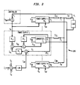
- FIGURE 2 illustrated is a modular power supply 200 employing one embodiment of a control system constructed according to the principles of the present invention.
- the modular power supply 200 includes ⁇ N> power supply modules PS 1 to PS N in parallel that deliver power to a common load LOAD. While the individual components of the power supply module PS j are illustrated and the operation thereof will hereinafter be described, the principles are equally applicable to the other power supply modules PS 1 to PS N employed by the modular power supply 200.
- the control system of the present invention includes an overall control circuit illustrated as the circuitry from the load LOAD through a controller CONTROLLER to a compensation circuit represented by a control box K j .
- the control system of the present invention also includes a separate module control circuit (associated with each power supply module PS 1 to PS N ) illustrated as compensation circuits represented by control blocks K j , B j , M j in the power supply module PS j .
- An overall output characteristic or load voltage V L is sensed and compared to a reference characteristic or reference voltage V DPV for the modular power supply 200 to generate an overall (or common) error signal or common error voltage V e that is sent to the power supply modules PS 1 to PS N .
- the output current I j of the power supply module PSj is sensed and compared to an average output current I AV of the power supply modules PS 1 to PS N and the resulting error signal is processed by the compensation circuit M j to yield a current error signal I ej .
- the current error signal I ej is derived representing a deviation of a ratio of the output current I j to a maximum output current capability I j(max) of the power supply module PS j from a ratio of an actual output current of the modular power supply 200 to a maximum output current of the modular power supply 200.
- the converter C j regulates an output characteristic or output voltage V j such that the difference V Rj - B j V j is approximately zero.
- the output voltage V j (processed by the compensation circuit B j ) combined with the reference voltage V Rj provides a regulating signal V Cj to control the converter C j to ultimately more precisely regulate the load voltage V L .
- the load voltage V L is approximately equal to the common reference voltage V DPV . Therefore, only the reference voltage V DPV need be adjusted to regulate the load voltage V L thereby avoiding the manual iterative process of the prior art.
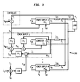
- FIGURE 3 illustrated is the modular power supply 200 of FIGURE 2 employing another embodiment of a control system constructed according to the principles of the present invention.
- the power supply 200 includes ⁇ N> power supply modules PS 1 to PSN in parallel that deliver power to a common load LOAD. While the individual components of the power supply module PS j are illustrated and the operation thereof will hereinafter be described, the principles are equally applicable to the other power supply modules PS 1 to PS N employed by the modular power supply 200.
- the control system of the present invention includes the overall control circuit and separate module control circuit (associated with each power supply module PS 1 to PS N ) as described with respect to FIGURE 2.
- the control system further includes a second characteristic reference or an additional reference voltage V REFj for the power supply modules PS 1 to PS N .
- the reference voltage V REFj is added to the common error voltage V e and the current error signal I ej to obtain the reference voltage V Rj for the converter C j .
- the converter C j regulates its output voltage V j so that the difference V Rj - B j V j is approximately zero.
- the output voltage V j (processed by the compensation circuit B j ) is also combined with the reference voltage V Rj to provide a regulating signal C cj to control the converter C j to ultimately more precisely regulate the load voltage V L .
- the load voltage V L is approximately equal to the common reference voltage V DPV thereby providing the advantages as described with respect to FIGURE 2.
- An additional advantage of the present embodiment is the added reliability provided with the second characteristic reference V REFj . Simply stated, if the common error voltage V e signal is interrupted, the load voltage V L will still be sufficiently regulated to an average output voltage of the power supply modules PS 1 to PS N less the voltage drops in the impedances Z Cj and Z j . This feature provides additional reliability for the power supply 200 while maintaining current sharing between the power supply modules PS 1 to PS N .
- FIGURE 4 illustrated is the modular power supply 200 of FIGURE 2 employing yet another embodiment of a control system constructed according to the principles of the present invention.
- the power supply 200 includes ⁇ N> power supply modules PS 1 to PS N in parallel that deliver power to a common load LOAD. While the individual components of the power supply module PS j are illustrated and the operation thereof will hereinafter be described, the principles are equally applicable to the other power supply modules PS 1 to PS N employed by the modular power supply 200.
- the control system of the present invention includes the overall control circuit and. separate module control circuit (associated with each power supply module PS 1 to PS N ) as described with respect to FIGURE 2.
- the load voltage V L is fed back to the compensation circuit B j of the power supply module PS j instead of the output voltage V j as illustrated with respect to FIGUREs 2 and 3.
- the control system therefore, improves regulation of the load voltage V L at the load LOAD when the common error voltage V e signal is interrupted.
- the load voltage V L is regulated at a level corresponding to an average of the power supply module PS 1 to PS N ; also, the voltage drops in the impedances Z Cj and Z P are effectively removed from the loop thereby further improving the regulation of the load voltage V L .
- FIGURE 5 illustrated is the modular power supply 200 of FIGURE 2 employing yet another embodiment of a control system constructed according to the principles of the present invention.
- the power supply 200 includes ⁇ N> power supply modules PS 1 to PS N in parallel that deliver power to a common load LOAD. While the individual components of the power supply module PS j are illustrated and the operation thereof will hereinafter be described, the principles are equally applicable to the other power supply modules PS 1 to PS N employed by the modular power supply 200.
- the control system of the present invention includes the overall control circuit and separate module control circuit (associated with each power supply module PS 1 to PS N ) as described with respect to FIGURE 2.
- the control system also includes (1) a first sample and hold circuit contained in an Analog-to-Digital ("A/D") converter, (2) an accumulator illustrated as a compensation circuit represented by a control box z -1 and (3) a second sample and hold circuit contained in the controller CONTROLLER.
- A/D Analog-to-Digital
- the load voltage V L is sampled and converted to a digital signal through an Analog-to-Digital ("A/D") converter.
- the digitized load voltage V L (n-1) is subtracted from the common reference value V DPV and the resulting common error voltage V e ( n -1) is sent to the power supply modules PS 1 to PS N periodically.
- the output currents I 1 (n-1) to I N ( n -1) from the power supply modules PS 1 to PS N are periodically digitized and an average value I AV ( n -1) is computed and sent to the power supply modules PS 1 to PSN periodically.
- the power supply module PS j derives a current error signal I ej ( n -1) by processing the difference between the average current I AV ( n -1) and the output current I j ( n -1) of the power supply module PS j via the compensation circuit M j .
- V Rj (n) V Rj ( n -1) + K j [V DPV -V L ( n -1)] + M j [I AV ( n -1) - I j ( n -1)]
- the voltage V Rj (n-1) serves as a reference that the voltage V j ( n -1) is regulated to through the power supply module PS j .
- the load voltage V L is precisely regulated to the desired level V DPV and the power supply modules PS 1 to PS N share the load LOAD.
- the control system of the present embodiment demonstrates improved noise immunity in the transmission of the common error voltage V e and the average current I AV because of the digital transmission of the signals in the power supply 200.
- the reference voltage V Rj ( n ) of the power supply module PS j is stored in digital memory thereby increasing the reliability of the power supply 200 in the event that the common error voltage V e or the average current I AV is interrupted.
- the power supply module PS j may employ the last stored value of the reference voltage V Rj ( n - 1 ) to regulate the output voltage V j ( n -1) of the converter C j and to maintain the load voltage V L at the desired level.
- the power supply modules PS 1 to PS N maintain current sharing provided that the load current remains relatively constant and the control parameters of the power supply modules PS 1 to PS N do not drift appreciably.
- FIGURE 6 illustrated is the modular power supply 200 of FIGURE 2 employing yet another embodiment of a control system constructed according to the principles of the present invention.
- the power supply 200 includes ⁇ N> power supply modules PS 1 to PS N in parallel that deliver power to a common load LOAD. While the individual components of the power supply module PS j are illustrated and the operation thereof will hereinafter be described, the principles are equally applicable to the other power supply modules PS 1 to PS N employed by the modular power supply 200.
- the control system of the present invention includes the overall control circuit and separate module control circuit (associated with each power supply module PS 1 to PS N ) as described with respect to FIGURE 2.
- the load current I L is sensed and compared with a reference signal I REF , representing a desired load current level, to generate a common load current error I REF -I L .
- the common load current error I REF -I L is sent to power supply modules Ps i to PS N .
- the output current I j of the power supply module PS j is sensed and compared to an average output current I AV and the resulting signal is processed by the compensation circuit M j to yield the current error signal I ej .
- the common load current error signal I REF -I L is processed by the compensation circuit K j and the resulting signal is added to the current error signal I ej to obtain the reference voltage V Rj for the converter C j .
- the converter C j regulates its output voltage V j so that the difference V Rj - B j V j is approximately zero.
- the output voltage V j (processed by the compensation circuit B j ) is also combined with the reference voltage V Rj to provide a regulating signal V Cj to control the converter C j .
- the load current I L is approximately equal to the reference current I REF . Therefore, only the reference current I REF need be adjusted to regulate the load current I L thereby avoiding the manual iterative process of the prior art.
Landscapes
- Engineering & Computer Science (AREA)
- Power Engineering (AREA)
- Direct Current Feeding And Distribution (AREA)
- Dc-Dc Converters (AREA)
- Control Of Voltage And Current In General (AREA)
Abstract
Description
- The present invention is directed, in general, to modular power supplies and, more specifically, to a control system that regulates an output and simultaneously sustains load sharing among power supply modules of the modular power supply.
- It is not uncommon to find a power supply having a plurality of slots for receiving individual power supply modules. The modular architecture provides several advantages, including, an increase in the level of power that may be delivered to a load and an increase in the overall reliability of the power supply by sharing the load requirements among a plurality of redundant power supply modules. Additionally, the modular architecture enhances the flexibility of the power supply by allowing individual modules to be replaced to accommodate changes in the power supply requirements. Finally, the modular architecture provides a robust system whereby failed modules can be rapidly replaced with replacement modules.
- Conventionally, the power supply may employ multiple converters in separate modules that convert an AC or DC input voltage to a DC output voltage. Again, the power supply may employ multiple converters in separate modules to increase the overall capacity and reliability of the power supply. The converters, in such a system, share the load to, among other things, evenly distribute stresses among the separate modules, while providing a regulated output to the load. Also, when a failure occurs in a modular system, it is possible to identify and shut down the failed unit without affecting the other parallel connected units, thereby minimizing the overall effects on the output of the power supply. While uniform power distribution or load sharing may be a goal of parallel converters in the modular power supply, several factors contribute to non-uniform distribution. For instance, as component tolerances and the characteristics of the components change due to uneven aging and different physical conditions, the power distribution therefrom also changes. Therefore, efforts should be made to adequately control the modules to regulate the output of the power supply and compensate for individual variations in the power supply modules.
- There are a number of alternatives well known in the prior art that attempt to achieve load sharing among parallel modules in a modular power supply. One of the simplest methods for load sharing is commonly referred to as the droop method. The droop method is an open-loop technique that programs the output impedance of the power supply modules to attain load sharing. A disadvantage of this type of technique is that there is poor regulation of the output voltage of the power supply. In addition, while this method obtains relatively acceptable load sharing at higher currents, at lower currents the droop method exhibits poor load sharing leading to large current imbalances between power supply modules.
- A second alternative is to select a master module to perform voltage control at the output of the power supply and force the remaining modules (i.e., slaves) to act as current sources. Since an error voltage is proportional to the load current, this alternative generally employs current-mode control. If the modules are similar in design then a given error voltage at the output, or error amplitude, will compel the modules to source the same load current. A major deficiency with the master/slave option is that if the master fails, the entire system is disabled thereby defeating the redundancy of the modular power supply.
- Another conventional method is a current sharing technique referred to as central limit control ("CLC"). The CLC design requires that the parallel modules regulate the voltage across the shared load and the voltage feedback loops of the modules sense the load voltage. As a result, the CLC provides voltage regulation at the output of the power supply and current sharing among the modules. There are several variations of this method including CLC with common voltage feedback and fixed reference voltage. Under this approach, the common output voltage across the shared load is regulated to a fixed reference through identical voltage error compensators. The operating control voltage that feeds the driver of each module is compensated by a corresponding error signal to produce current sharing among the power supply modules. While this alternative provides adequate load sharing for identical power supply modules, it cannot adequately compensate for variations in the individual power supply modules (e.g., variations in tolerances) due to the non-identical compensators employed therein.
- Accordingly, what is needed in the art is a control system for a modular power supply that maintains a well regulated output and employs current sharing among the power supply modules, while compensating for variations in the performance and tolerances of the individual power supply modules.
- To address the above-discussed deficiencies of the prior art, the present invention provides, in a modular power supply having a plurality of module slots capable of receiving power supply modules therein, a system and method for controlling the power supply modules to regulate an overall output characteristic of the modular power supply.
- The system includes: (1) an overall control circuit for sensing the overall output characteristic of the modular power supply and developing therefrom an overall error signal representing a deviation of the overall output characteristic from a reference characteristic and (2) a separate module control circuit for each of the power supply modules, each separate module control circuit sensing an output characteristic of an associated power supply module and developing therefrom and from the overall error signal a regulating signal for the associated power supply module. The regulating signal controls the output characteristic of the associated power supply module to control the overall output characteristic of the modular power supply.
- The system of the present invention provides precise regulation of the overall output characteristic of the modular power supply, while concurrently maintaining load sharing among the power supply modules of the power supply. The system attains this higher level of regulation by employing both system-wide and individual modular control. The overall control circuit develops the overall or common error signal that the module control circuits employ, in conjunction with an output characteristic of the individual module, to develop a regulating signal that controls the output of each power supply module. By selecting the gain of the compensation circuits to adequately amplify the common error signal, the output characteristic can be regulated to track the reference characteristic very closely. The system performance can be achieved despite changes in the load, errors in sensing the output characteristic of any particular power supply module, variations in the tolerances of the power supply components or variations in the gains of the compensation circuits employed in the power supply.
- In an alternative embodiment of the present invention, the separate module control circuit senses an output current of the associated power supply module and develops therefrom a current error signal representing a deviation from an average of output currents of the power supply modules. The separate module control circuit combines the current error signal with the overall error signal to further develop the regulating signal. In a related, but alternative embodiment of the present invention, the separate module control circuit senses an actual output current of the associated power supply module and develops therefrom a current error signal representing a deviation of a ratio of the actual output current to a maximum output current of the associated power supply module from a ratio of an actual output current of the modular power supply to a maximum output current of the modular power supply. Again, the separate module control circuit combines the current error signal with the overall error signal to further develop said regulating signal. The system of the present invention is compatible with a modular power supply employing non-identical power supply modules (e.g., the power supply modules have varying maximum current carrying capability). In either embodiment, the separate module control circuit derives the regulating signal from the output characteristic of the associated power supply module, the overall error signal and the current error signal.
- In an alternative embodiment of the present invention, the separate module control circuit develops the regulating signal from a second characteristic reference signal of the associated power supply module. The regulating signal is derived with the addition of the second characteristic reference thereby increasing the reliability of the overall system. For instance, if the common error signal is interrupted, the power supply modules may still develop the regulating signal to control an output therefrom and the overall output characteristic of the power supply.
- In an alternative embodiment of the present invention, the separate module control circuit develops the regulating signal directly from the overall output characteristic. By developing the regulating signal from the overall output characteristic, the reliability of the system is enhanced to accommodate unforeseen conditions such as when the common error signal is interrupted.
- In an alternative embodiment of the present invention, the system includes: (1) a first sample and hold circuit for receiving and temporarily storing the overall output characteristic, the overall control circuit developing therefrom a sampled overall error signal, (2) a second sample and hold circuit for receiving and temporarily storing an output current of the associated power supply module, the separate module control circuit developing therefrom a sampled current error signal representing a deviation from an average of output currents of the power supply modules and (3) an accumulator, associated with the separate module control circuit, for generating an intermediate regulating signal from the sampled overall error signal and said sampled current error signal. In a related, but alternative embodiment of the present invention, the sampled current error signal represents a deviation of a ratio of an actual output current to a maximum output current of the associated power supply module from a ratio of an actual output current of the modular power supply to a maximum output current of the modular power supply. In either case, the intermediate regulating signal is derived from an accumulated and sampled overall error signal and current error signal. The present embodiments provide several advantages, namely, the capability to'more precisely regulate the overall output characteristic of the modular power supply and the ability to maintain the regulating signal at the last known value in the event of a failure of the overall control circuit.
- In an alternative embodiment of the present invention, the overall output characteristic is a function of an output voltage of the modular power supply. One of ordinary skill in the pertinent art should understand that other electrical characteristics, such as, without limitation, an output current, may also serve as the overall output characteristic of the modular power supply.
- Another aspect of the present invention is, for use in a modular power supply having a plurality of module slots capable of receiving power supply modules therein and an overall control circuit for sensing an overall output characteristic of the modular power supply and developing therefrom an overall error signal representing a deviation of the overall output characteristic from a reference characteristic, a power supply module, including: (1) power conversion circuitry and (2) a module control circuit constructed according to the principles of the present invention. One of ordinary skill in the pertinent art should understand that the power conversion circuitry includes any circuitry, such as, without limitation, a DC/DC power converter, that transforms one form of electrical power to another.
- The foregoing has outlined, rather broadly, preferred and alternative features of the present invention so that those skilled in the art may better understand the detailed description of the invention that follows. Additional features of the invention will be described hereinafter that form the subject of the claims of the invention. Those skilled in the art should appreciate that they can readily use the disclosed conception and specific embodiment as a basis for designing or modifying other structures for carrying out the same purposes of the present invention. Those skilled in the art should also realize that such equivalent constructions do not depart from the spirit and scope of the invention in its broadest form.
- For a more complete understanding of the present invention, reference is now made to the following descriptions taken in conjunction with the accompanying drawings, in which:
- FIGURE 1 illustrates a prior art control system for a modular power supply;
- FIGURE 2 illustrates a modular power supply employing one embodiment of a control system constructed according to the principles of the present invention;
- FIGURE 3 illustrates the modular power supply of FIGURE 2 employing another embodiment of a control system constructed according to the principles of the present invention;
- FIGURE 4 illustrates the modular power supply of FIGURE 2 employing yet another embodiment of a control system constructed according to the principles of the present invention;
- FIGURE 5 illustrates the modular power supply of FIGURE 2 employing yet another embodiment of a control system constructed according to the principles of the present invention; and
- FIGURE 6 illustrates the modular power supply of FIGURE 2 employing yet another embodiment of a control system constructed according to the principles of the present invention.
- Referring initially to FIGURE 1, illustrated is a prior art control system for a
modular power supply 100. Thepower supply 100 includes <N> power supply modules PS1 to PSN in parallel that deliver power to a common load LOAD. While the individual components of the power supply module PSj are illustrated and the operation thereof will hereinafter be described, the principles are equally applicable to the other power supply modules PS1 to PSN employed by themodular power supply 100. - The power supply module PSj is connected in series with a interconnection impedance Z cj and a common interconnection impedance Zp to the load LOAD. The load voltage V L is sensed and sent to the power supply module PSj. · The output current I j of the power supply module PSj is compared with a signal equal to the average output current I AV of all the power supplies PS1 to PSN; a resulting error signal is processed by a compensation circuit represented by a control block M j to yield a current error signal for the power supply module PSj. The current error signal is added to the reference voltage V REFj to create a voltage V Rj . The voltage V Rj is compared to the common fed back load voltage V L , processed by a compensation circuit represented by a control block B j , and the resulting voltage is used to control an output voltage V j of the power supply module PSj.
- In this prior art control system, the power supply modules PS1 to PSN share the load current and the load voltage V L is regulated at a level that is an average of the individual power supply module reference voltages. The dependence of the load voltage V L on the average value of the individual power supply modules reference voltages makes precise regulation of the load voltage V L very difficult. If the load voltage V L needs to be adjusted, then the reference voltage of each power supply module PS1 to PSN must be adjusted via a manual iterative process until the desired level of the load voltage V L is obtained and all of the power supply modules PS1 to PSN are delivering the same current. When the power supply modules PS1 to PSN are added or removed from the
modular power supply 100, this manual iterative process must be repeated. - Turning now to FIGURE 2, illustrated is a
modular power supply 200 employing one embodiment of a control system constructed according to the principles of the present invention. Analogous to themodular power supply 100 of FIGURE 1, themodular power supply 200 includes <N> power supply modules PS1 to PSN in parallel that deliver power to a common load LOAD. While the individual components of the power supply module PSj are illustrated and the operation thereof will hereinafter be described, the principles are equally applicable to the other power supply modules PS1 to PSN employed by themodular power supply 200. The control system of the present invention includes an overall control circuit illustrated as the circuitry from the load LOAD through a controller CONTROLLER to a compensation circuit represented by a control box K j . The control system of the present invention also includes a separate module control circuit (associated with each power supply module PS1 to PSN) illustrated as compensation circuits represented by control blocks K j , B j , M j in the power supply module PS j . - An overall output characteristic or load voltage V L is sensed and compared to a reference characteristic or reference voltage V DPV for the
modular power supply 200 to generate an overall (or common) error signal or common error voltage V e that is sent to the power supply modules PS1 to PSN. The output current I j of the power supply module PSj is sensed and compared to an average output current I AV of the power supply modules PS1 to PSN and the resulting error signal is processed by the compensation circuit M j to yield a current error signal I ej . If the power supply modules PS1 to PSN have varying maximum current capabilities, the current error signal I ej is derived representing a deviation of a ratio of the output current I j to a maximum output current capability I j(max) of the power supply module PSj from a ratio of an actual output current of themodular power supply 200 to a maximum output current of themodular power supply 200. In either case, the common error voltage V e (where V e = V L - V DPV ) is processed by the compensation circuit K j and the resulting signal is added to the current error signal I ej to obtain the reference voltage V Rj for a converter C j (i.e., the power conversion circuitry). The converter C j regulates an output characteristic or output voltage V j such that the difference V Rj - B j V j is approximately zero. The output voltage V j (processed by the compensation circuit Bj) combined with the reference voltage V Rj provides a regulating signal V Cj to control the converter C j to ultimately more precisely regulate the load voltage V L . By adjusting the gains of the compensation circuit K j to be relatively large, the load voltage V L is approximately equal to the common reference voltage V DPV . Therefore, only the reference voltage V DPV need be adjusted to regulate the load voltage V L thereby avoiding the manual iterative process of the prior art. - Turning now to FIGURE 3, illustrated is the
modular power supply 200 of FIGURE 2 employing another embodiment of a control system constructed according to the principles of the present invention. Again, thepower supply 200 includes <N> power supply modules PS1 to PSN in parallel that deliver power to a common load LOAD. While the individual components of the power supply module PSj are illustrated and the operation thereof will hereinafter be described, the principles are equally applicable to the other power supply modules PS1 to PSN employed by themodular power supply 200. The control system of the present invention includes the overall control circuit and separate module control circuit (associated with each power supply module PS1 to PSN) as described with respect to FIGURE 2. - The control system further includes a second characteristic reference or an additional reference voltage V REFj for the power supply modules PS1 to PSN. The reference voltage V REFj is added to the common error voltage V e and the current error signal I ej to obtain the reference voltage V Rj for the converter C j . Again, the converter C j regulates its output voltage V j so that the difference V Rj - B j V j is approximately zero. The output voltage V j (processed by the compensation circuit B j ) is also combined with the reference voltage V Rj to provide a regulating signal C cj to control the converter C j to ultimately more precisely regulate the load voltage V L . Analogous to the control system of FIGURE 2, by adjusting the gain of the compensation circuit K j to be relatively large, the load voltage V L is approximately equal to the common reference voltage V DPV thereby providing the advantages as described with respect to FIGURE 2. An additional advantage of the present embodiment is the added reliability provided with the second characteristic reference V REFj . Simply stated, if the common error voltage V e signal is interrupted, the load voltage V L will still be sufficiently regulated to an average output voltage of the power supply modules PS1 to PSN less the voltage drops in the impedances Z Cj and Z j . This feature provides additional reliability for the
power supply 200 while maintaining current sharing between the power supply modules PS1 to PSN. - Turning now to FIGURE 4, illustrated is the
modular power supply 200 of FIGURE 2 employing yet another embodiment of a control system constructed according to the principles of the present invention. Again, thepower supply 200 includes <N> power supply modules PS1 to PSN in parallel that deliver power to a common load LOAD. While the individual components of the power supply module PSj are illustrated and the operation thereof will hereinafter be described, the principles are equally applicable to the other power supply modules PS1 to PSN employed by themodular power supply 200. The control system of the present invention includes the overall control circuit and. separate module control circuit (associated with each power supply module PS1 to PSN) as described with respect to FIGURE 2. - For purposes of the present embodiment, the load voltage V L is fed back to the compensation circuit B j of the power supply module PSj instead of the output voltage V j as illustrated with respect to FIGUREs 2 and 3. The control system, therefore, improves regulation of the load voltage V L at the load LOAD when the common error voltage V e signal is interrupted. Under such circumstances, the load voltage V L is regulated at a level corresponding to an average of the power supply module PS1 to PSN; also, the voltage drops in the impedances Z Cj and Z P are effectively removed from the loop thereby further improving the regulation of the load voltage V L .
- Turning now to FIGURE 5, illustrated is the
modular power supply 200 of FIGURE 2 employing yet another embodiment of a control system constructed according to the principles of the present invention. Again, thepower supply 200 includes <N> power supply modules PS1 to PSN in parallel that deliver power to a common load LOAD. While the individual components of the power supply module PSj are illustrated and the operation thereof will hereinafter be described, the principles are equally applicable to the other power supply modules PS1 to PSN employed by themodular power supply 200. The control system of the present invention includes the overall control circuit and separate module control circuit (associated with each power supply module PS1 to PSN) as described with respect to FIGURE 2. The control system, as illustrated in the present embodiment, also includes (1) a first sample and hold circuit contained in an Analog-to-Digital ("A/D") converter, (2) an accumulator illustrated as a compensation circuit represented by a control box z -1 and (3) a second sample and hold circuit contained in the controller CONTROLLER. - The load voltage V L is sampled and converted to a digital signal through an Analog-to-Digital ("A/D") converter. The digitized load voltage V L (n-1) is subtracted from the common reference value V DPV and the resulting common error voltage V e (n-1) is sent to the power supply modules PS1 to PSN periodically. In addition, the output currents I 1 (n-1) to I N (n-1) from the power supply modules PS1 to PSN, respectively, are periodically digitized and an average value I AV (n-1) is computed and sent to the power supply modules PS1 to PSN periodically. The power supply module PSj, for instance, then derives a current error signal I ej (n-1) by processing the difference between the average current I AV (n-1) and the output current I j (n-1) of the power supply module PSj via the compensation circuit M j . The (n-1) sample of the power supply module's reference voltage or intermediate regulating signal V Rj (n-1) is obtained through the following equation:

power supply 200. Additionally, the reference voltage V Rj (n) of the power supply module PSj is stored in digital memory thereby increasing the reliability of thepower supply 200 in the event that the common error voltage V e or the average current I AV is interrupted. Under these circumstances, the power supply module PSj may employ the last stored value of the reference voltage V Rj (n-1) to regulate the output voltage V j (n-1) of the converter C j and to maintain the load voltage V L at the desired level. Also, the power supply modules PS1 to PSN maintain current sharing provided that the load current remains relatively constant and the control parameters of the power supply modules PS1 to PSN do not drift appreciably. - Turning now to FIGURE 6, illustrated is the
modular power supply 200 of FIGURE 2 employing yet another embodiment of a control system constructed according to the principles of the present invention. Again, thepower supply 200 includes <N> power supply modules PS1 to PSN in parallel that deliver power to a common load LOAD. While the individual components of the power supply module PSj are illustrated and the operation thereof will hereinafter be described, the principles are equally applicable to the other power supply modules PS1 to PSN employed by themodular power supply 200. The control system of the present invention includes the overall control circuit and separate module control circuit (associated with each power supply module PS1 to PSN) as described with respect to FIGURE 2. - In the illustrated embodiment, the load current I L is sensed and compared with a reference signal I REF , representing a desired load current level, to generate a common load current error I REF -I L . The common load current error I REF -I L is sent to power supply modules Psi to PSN. The output current I j of the power supply module PSj is sensed and compared to an average output current I AV and the resulting signal is processed by the compensation circuit M j to yield the current error signal I ej . The common load current error signal I REF -I L is processed by the compensation circuit K j and the resulting signal is added to the current error signal I ej to obtain the reference voltage V Rj for the converter C j . Again, the converter C j regulates its output voltage V j so that the difference V Rj -B j V j is approximately zero. The output voltage V j (processed by the compensation circuit B j ) is also combined with the reference voltage V Rj to provide a regulating signal V Cj to control the converter C j . By adjusting the gains of the compensation circuit K j to be relatively large, the load current I L is approximately equal to the reference current I REF . Therefore, only the reference current I REF need be adjusted to regulate the load current I L thereby avoiding the manual iterative process of the prior art.
- Although the present invention has been described in detail, those skilled in the art should understand that they can make various changes, substitutions and alterations herein without departing from the spirit and scope of the invention in its broadest form.
Claims (10)
- In a modular power supply having a plurality of module slots capable of receiving power supply modules therein, a system for controlling said power supply modules to regulate an overall output characteristic of said modular power supply, comprising:an overall control circuit for sensing said overall output characteristic of said modular power supply and developing therefrom an overall error signal representing a deviation of said overall output characteristic from a reference characteristic; anda separate module control circuit for each of said power supply modules, said separate module control circuit sensing an output characteristic of an associated power supply module and developing therefrom and from said overall error signal a regulating signal for said associated power supply module, said regulating signal controlling said output characteristic of said associated power supply module to control said overall output characteristic of said modular power supply.
- The system as recited in Claim 1 wherein said separate module control circuit senses an output current of said associated power supply module and develops therefrom a current error signal representing a deviation from an average of output currents of said power supply modules, said separate module control circuit combining said current error signal with said overall error signal to further develop said regulating signal.
- The system as recited in Claim 1 wherein said separate module control circuit senses an actual output current of said associated power supply module and develops therefrom a current error signal representing a deviation of:a ratio of said actual output current to a maximum output current of said associated power supply module froma ratio of an actual output current of said modular power supply to a maximum output current of said modular power supply,said separate module control circuit combining said current error signal with said overall error signal to further develop said regulating signal.
- The system as recited in Claim 1 wherein said separate module control circuit develops said regulating signal from a second characteristic reference signal of said associated power supply module.
- The system as recited in Claim 1 wherein said separate module control circuit develops said regulating signal directly from said overall output characteristic.
- The system as recited in Claim 1, further comprising:a first sample and hold circuit for receiving and temporarily storing said overall output characteristic, said overall control circuit developing therefrom a sampled overall error signal;a second sample and hold circuit for receiving and temporarily storing an output current of said associated power supply module, said separate module control circuit developing therefrom a sampled current error signal representing a deviation from an average of output currents of said power supply modules; andan accumulator, associated with said separate module control circuit, for generating an intermediate regulating signal from said sampled overall error signal and said sampled current error signal.
- The system as recited in Claim 1, further comprising:a first sample and hold circuit for receiving and temporarily storing said overall output characteristic, said overall control circuit developing therefrom a sampled overall error signal;a second sample and hold circuit for receiving and temporarily storing an actual output current of said associated power supply module, said separate module control circuit developing therefrom a sampled current error signal representing a deviation of:a ratio of said actual output current to a maximum output current of said associated power supply module froma ratio of an actual output current of said modular power supply to a maximum output current of said modular power supply; andan accumulator, associated with said separate module control circuit, for generating of an intermediate regulating signal from said sampled overall error signal and said sampled current error signal.
- The system as recited in Claim 1 wherein said overall output characteristic is a function of an output voltage of said modular power supply.
- The system as recited in Claim 1 wherein said overall output characteristic is a function of an output recurrent of said modular power supply.
- The system as recited in Claim 1 wherein said each of said power supply modules comprises power conversion circuitry coupled to an output of said modular power supply via an impedance network.
Applications Claiming Priority (2)
| Application Number | Priority Date | Filing Date | Title |
|---|---|---|---|
| US08/655,334 US5740023A (en) | 1996-05-24 | 1996-05-24 | Control system for a modular power supply and method of operation thereof |
| US655334 | 1996-05-24 |
Publications (2)
| Publication Number | Publication Date |
|---|---|
| EP0809347A2 true EP0809347A2 (en) | 1997-11-26 |
| EP0809347A3 EP0809347A3 (en) | 1999-07-07 |
Family
ID=24628472
Family Applications (1)
| Application Number | Title | Priority Date | Filing Date |
|---|---|---|---|
| EP97303253A Withdrawn EP0809347A3 (en) | 1996-05-24 | 1997-05-13 | Control system for a modular power supply and method of operation thereof |
Country Status (2)
| Country | Link |
|---|---|
| US (1) | US5740023A (en) |
| EP (1) | EP0809347A3 (en) |
Cited By (8)
| Publication number | Priority date | Publication date | Assignee | Title |
|---|---|---|---|---|
| WO2001037413A3 (en) * | 1999-11-15 | 2001-12-20 | Semtech Corp | Multi-phase and multi-module power supplies with balanced current between phases and modules |
| EP1248354A1 (en) * | 2001-04-06 | 2002-10-09 | Intersil Corporation | Multi-phase converter with balanced currents |
| USRE38454E1 (en) | 1999-09-01 | 2004-03-09 | Intersil Communications, Inc. | Multi-phase converter with balanced currents |
| EP1473820A3 (en) * | 2003-04-29 | 2006-02-15 | Texas Instruments Inc. | Multi-phase and multi-module power system with a current share bus |
| WO2006022675A1 (en) * | 2004-07-30 | 2006-03-02 | Raytheon Company | Method and apparatus for a power system for phased-array radar |
| EP1241776A4 (en) * | 2000-10-02 | 2007-09-26 | Omron Tateisi Electronics Co | Power supply |
| US7508093B2 (en) | 2002-12-23 | 2009-03-24 | Huettinger Elektronik Gmbh + Co. Kg | Modular current supply |
| EP2963800A1 (en) * | 2014-07-02 | 2016-01-06 | Siemens Aktiengesellschaft | Controlling parallel converter systems for wind turbines |
Families Citing this family (26)
| Publication number | Priority date | Publication date | Assignee | Title |
|---|---|---|---|---|
| US5909591A (en) * | 1996-06-18 | 1999-06-01 | Lucent Technologies Inc. | System and method for identifying individual modules in a modular system |
| US5905645A (en) * | 1996-12-02 | 1999-05-18 | Astec International Limited | Thermally aided power sharing of power supplies with or without an external current share line |
| JP3145942B2 (en) * | 1997-02-18 | 2001-03-12 | 日本電気株式会社 | Power system |
| DE19720948A1 (en) * | 1997-05-17 | 1998-11-19 | Bosch Gmbh Robert | Voltage conversion device |
| US5875104A (en) * | 1997-06-26 | 1999-02-23 | Vlt Corporation | Operating switching power converters in a phased power sharing array |
| JPH11135860A (en) * | 1997-10-31 | 1999-05-21 | Mitsubishi Electric Corp | Pulse laser excitation control method and power supply device for pulse laser excitation |
| FI107418B (en) | 1998-05-22 | 2001-07-31 | Muuntolaite Oy | Method and plant for controlling a power source system |
| US6134129A (en) * | 1998-09-23 | 2000-10-17 | Ro Associates | Current sharing signal coupling/decoupling circuit for power converter systems |
| AU2432701A (en) * | 1999-12-16 | 2001-06-25 | Mcandrews Enterprises Inc. | Spare bus power plant |
| US6381155B1 (en) * | 2000-05-23 | 2002-04-30 | Next Power Corporation | Method for clusterized power sharing conversion and regulation of the primary power source within a converting and regulating power supply, and system |
| US6664659B1 (en) * | 2000-07-03 | 2003-12-16 | Scientific-Atlanta, Inc. | CATV amplifier power supply redundancy |
| US20040239188A1 (en) * | 2003-05-28 | 2004-12-02 | Hewlett-Packard Development Company, L.P. | Power supply load balancing apparatus |
| TWI234326B (en) * | 2003-12-30 | 2005-06-11 | Delta Electronics Inc | Master-slave current distribution circuit |
| DE102004016123B4 (en) * | 2004-04-01 | 2012-03-22 | Siemens Ag | Method for monitoring supply processes in consumers and device therefor |
| US8730695B1 (en) | 2006-03-02 | 2014-05-20 | Ocean Server Technology, Inc. | Load balancing method and system to scale DC output power by temperature of parallel DC power supplies |
| US8150540B2 (en) | 2008-09-17 | 2012-04-03 | Lineage Power Corporation | Controller and method for controlling converters of disparate type |
| US20100077238A1 (en) * | 2008-09-25 | 2010-03-25 | Wisconsin Alumni Research Foundation | Energy efficienct power supply system |
| US8193661B2 (en) * | 2009-02-17 | 2012-06-05 | Lineage Power Corporation | DC plant controller and method for selecting among multiple power sources and DC plant employing the same |
| JP4783453B2 (en) * | 2009-09-10 | 2011-09-28 | 力也 阿部 | Multi-terminal type asynchronous interconnection device, power equipment control terminal device, power network system and control method therefor |
| US8325504B2 (en) * | 2009-09-18 | 2012-12-04 | Power Distribution, Inc. | Direct current power supply for mission critical applications |
| US20130073881A1 (en) * | 2011-09-20 | 2013-03-21 | Silverstone Technology Co., Ltd. | Extensible external power supply |
| CN105990999A (en) * | 2015-01-27 | 2016-10-05 | 台达电子工业股份有限公司 | Power supply device and control method thereof |
| US20170141684A1 (en) * | 2015-11-18 | 2017-05-18 | Intersil Americas LLC | Method and System for DC-DC Voltage Converters |
| US10110127B2 (en) | 2015-12-04 | 2018-10-23 | Intersil Americas LLC | Method and system for DC-DC voltage converters |
| US9785166B2 (en) | 2015-12-14 | 2017-10-10 | Intersil Americas LLC | Method and system for DC-DC voltage converters |
| CN113640573B (en) * | 2020-05-11 | 2025-02-21 | 台达电子工业股份有限公司 | Methods for inspecting power units |
Family Cites Families (22)
| Publication number | Priority date | Publication date | Assignee | Title |
|---|---|---|---|---|
| US3648147A (en) * | 1970-11-12 | 1972-03-07 | Gen Electric | Starting control scheme for rectifier-inverter systems |
| FR2163253A5 (en) * | 1972-02-21 | 1973-07-20 | Siemens Ag | |
| US4451773A (en) * | 1982-04-02 | 1984-05-29 | Bell Telephone Laboratories, Incorporated | Rectifier control system for a DC power plant system |
| US4468722A (en) * | 1982-07-28 | 1984-08-28 | Reliance Electric Company | Power supply having slope controlled output volt-ampere characteristic |
| US4635178A (en) * | 1983-11-04 | 1987-01-06 | Ceag Electric Corp. | Paralleled DC power supplies sharing loads equally |
| US4717833A (en) * | 1984-04-30 | 1988-01-05 | Boschert Inc. | Single wire current share paralleling of power supplies |
| US4814965A (en) * | 1987-09-30 | 1989-03-21 | Spectra Physics | High power flyback, variable output voltage, variable input voltage, decoupled power supply |
| US4924170A (en) * | 1989-01-03 | 1990-05-08 | Unisys Corporation | Current sharing modular power supply |
| US5200643A (en) * | 1989-02-21 | 1993-04-06 | Westinghouse Electric Corp. | Parallel electric power supplies with current sharing and redundancy |
| US5338994A (en) * | 1989-07-20 | 1994-08-16 | General Electric Company | Method and apparatus for achieving current balance in parallel connected switching devices |
| DE3932437C1 (en) * | 1989-09-28 | 1990-10-04 | Bicc-Vero Elektronics Gmbh, 2800 Bremen, De | |
| DE3941052C1 (en) * | 1989-12-12 | 1991-05-29 | Siemens Ag, 1000 Berlin Und 8000 Muenchen, De | |
| US5164890A (en) * | 1990-03-29 | 1992-11-17 | Hughes Aircraft Company | Current share scheme for parallel operation of power conditioners |
| IT1244911B (en) * | 1991-01-31 | 1994-09-13 | Texas Instruments Italia Spa | PHYSICALLY INSERABLE NEURONIC NETWORK ARCHITECTURE IN THE LEARNING PROCESS. |
| US5157269A (en) * | 1991-01-31 | 1992-10-20 | Unitrode Corporation | Load current sharing circuit |
| FR2678397B1 (en) * | 1991-06-25 | 1993-09-03 | Cegelec | REDUCING TYPE DISTURBANCE LIMITING DEVICE FOR REGULATING EQUIPMENT. |
| US5319536A (en) * | 1991-12-17 | 1994-06-07 | International Business Machines Corporation | Power system for parallel operation of AC/DC convertrs |
| JPH0798620A (en) * | 1992-11-13 | 1995-04-11 | Seiko Epson Corp | Electronic device and computer using the same |
| US5428523A (en) * | 1993-03-30 | 1995-06-27 | Ro Associates | Current sharing signal coupling/decoupling circuit for power converter systems |
| US5638264A (en) * | 1993-12-27 | 1997-06-10 | Hitachi, Ltd. | Parallelized power supply system providing uninterrupted operation |
| DE4401728A1 (en) * | 1994-01-21 | 1995-08-03 | Siemens Nixdorf Inf Syst | Current balancing circuit |
| US5672958A (en) * | 1995-11-14 | 1997-09-30 | Dell Usa L.P. | Method and apparatus for modifying feedback sensing for a redundant power supply system |
-
1996
- 1996-05-24 US US08/655,334 patent/US5740023A/en not_active Expired - Lifetime
-
1997
- 1997-05-13 EP EP97303253A patent/EP0809347A3/en not_active Withdrawn
Cited By (13)
| Publication number | Priority date | Publication date | Assignee | Title |
|---|---|---|---|---|
| USRE38454E1 (en) | 1999-09-01 | 2004-03-09 | Intersil Communications, Inc. | Multi-phase converter with balanced currents |
| USRE42063E1 (en) | 1999-09-01 | 2011-01-25 | Intersil Americas Inc. | Multi-phase converter with balanced currents |
| WO2001037413A3 (en) * | 1999-11-15 | 2001-12-20 | Semtech Corp | Multi-phase and multi-module power supplies with balanced current between phases and modules |
| EP1241776A4 (en) * | 2000-10-02 | 2007-09-26 | Omron Tateisi Electronics Co | Power supply |
| EP1248354A1 (en) * | 2001-04-06 | 2002-10-09 | Intersil Corporation | Multi-phase converter with balanced currents |
| US7508093B2 (en) | 2002-12-23 | 2009-03-24 | Huettinger Elektronik Gmbh + Co. Kg | Modular current supply |
| EP1473820A3 (en) * | 2003-04-29 | 2006-02-15 | Texas Instruments Inc. | Multi-phase and multi-module power system with a current share bus |
| AU2004322718B2 (en) * | 2004-07-30 | 2009-02-05 | Raytheon Company | Method and apparatus for a power system for phased-array radar |
| WO2006022675A1 (en) * | 2004-07-30 | 2006-03-02 | Raytheon Company | Method and apparatus for a power system for phased-array radar |
| EP2963800A1 (en) * | 2014-07-02 | 2016-01-06 | Siemens Aktiengesellschaft | Controlling parallel converter systems for wind turbines |
| CN105226958A (en) * | 2014-07-02 | 2016-01-06 | 西门子公司 | Parallel inverter system for wind turbine is controlled |
| US9531290B2 (en) | 2014-07-02 | 2016-12-27 | Siemens Aktiengesellschaft | Controlling parallel converter systems for wind turbines |
| CN105226958B (en) * | 2014-07-02 | 2019-08-20 | 西门子公司 | Controlling parallel converter systems for wind turbines |
Also Published As
| Publication number | Publication date |
|---|---|
| EP0809347A3 (en) | 1999-07-07 |
| US5740023A (en) | 1998-04-14 |
Similar Documents
| Publication | Publication Date | Title |
|---|---|---|
| US5740023A (en) | Control system for a modular power supply and method of operation thereof | |
| US7773395B2 (en) | Uniform converter input voltage distribution power system | |
| US6009000A (en) | Shared-bus current sharing parallel connected current-mode DC to DC converters | |
| US5157269A (en) | Load current sharing circuit | |
| US6958552B2 (en) | Failsafe power oring with current sharing | |
| EP0315366B1 (en) | A regulated dc power supply having master and slave regulators | |
| JP2667345B2 (en) | N + 1 power supply system | |
| US5493154A (en) | Temperature share scheme | |
| US6281485B1 (en) | Maximum power tracking solar power system | |
| US4877972A (en) | Fault tolerant modular power supply system | |
| US6885236B2 (en) | Reference ladder having improved feedback stability | |
| US5550461A (en) | System for operating a plurality of power supply modules in parallel | |
| US8645726B2 (en) | Method and system for load sharing in a multiple power supply system | |
| US7964991B2 (en) | Converter channelized uniform power distribution system | |
| US11664724B1 (en) | Power bus voltage drop compensation using sampled bus resistance determination | |
| US8148850B2 (en) | Device for balancing the power supplied by power generators | |
| SE510611C2 (en) | BUCK-BOOST VOLTAGE REGULATOR | |
| US6229291B1 (en) | Current sharing control system of power supply and output voltage sensing circuit | |
| KR20120067988A (en) | Method for controling output volatge of power supply apparatus for multi-output, power supply apparatus for multi-output, and image forming apparatus having it | |
| Moussaoui et al. | An overview of the control scheme for distributed power systems | |
| US6191569B1 (en) | Circuit and method for generating estimated feedback for the controller of a slave power module in a master/slave paralleling scheme | |
| US5864476A (en) | Power supply apparatus | |
| CN113674661B (en) | Debugging circuit, debugging method and debugging device for displaying module reference voltage | |
| GB2122776A (en) | Power supplies with parallel supply modules | |
| CN1096730C (en) | Circuit for a coupled, linearly re-adjusted electricity supply unit supplying output voltage |
Legal Events
| Date | Code | Title | Description |
|---|---|---|---|
| PUAI | Public reference made under article 153(3) epc to a published international application that has entered the european phase |
Free format text: ORIGINAL CODE: 0009012 |
|
| AK | Designated contracting states |
Kind code of ref document: A2 Designated state(s): DE FR GB |
|
| PUAL | Search report despatched |
Free format text: ORIGINAL CODE: 0009013 |
|
| AK | Designated contracting states |
Kind code of ref document: A3 Designated state(s): DE FR GB |
|
| 17P | Request for examination filed |
Effective date: 19991210 |
|
| 17Q | First examination report despatched |
Effective date: 20040423 |
|
| STAA | Information on the status of an ep patent application or granted ep patent |
Free format text: STATUS: THE APPLICATION IS DEEMED TO BE WITHDRAWN |
|
| 18D | Application deemed to be withdrawn |
Effective date: 20041104 |