EP0794677A2 - Method and circuit arrangement for separating luminance and chrominance signals from a composite colour signal - Google Patents
Method and circuit arrangement for separating luminance and chrominance signals from a composite colour signal Download PDFInfo
- Publication number
- EP0794677A2 EP0794677A2 EP97103172A EP97103172A EP0794677A2 EP 0794677 A2 EP0794677 A2 EP 0794677A2 EP 97103172 A EP97103172 A EP 97103172A EP 97103172 A EP97103172 A EP 97103172A EP 0794677 A2 EP0794677 A2 EP 0794677A2
- Authority
- EP
- European Patent Office
- Prior art keywords
- signals
- values
- signal
- lines
- distance
- Prior art date
- Legal status (The legal status is an assumption and is not a legal conclusion. Google has not performed a legal analysis and makes no representation as to the accuracy of the status listed.)
- Granted
Links
Images


Classifications
-
- H—ELECTRICITY
- H04—ELECTRIC COMMUNICATION TECHNIQUE
- H04N—PICTORIAL COMMUNICATION, e.g. TELEVISION
- H04N9/00—Details of colour television systems
- H04N9/77—Circuits for processing the brightness signal and the chrominance signal relative to each other, e.g. adjusting the phase of the brightness signal relative to the colour signal, correcting differential gain or differential phase
- H04N9/78—Circuits for processing the brightness signal and the chrominance signal relative to each other, e.g. adjusting the phase of the brightness signal relative to the colour signal, correcting differential gain or differential phase for separating the brightness signal or the chrominance signal from the colour television signal, e.g. using comb filter
Definitions
- the invention relates to a method and a circuit arrangement for separating luminance and chrominance signals of a CVBS signal, in particular a comb filter arrangement for PAL signals.
- the transmitted CVBS signal consists of luminance and chrominance signals.
- the chrominance signal in turn is composed of two color difference signals (U / V signals for PAL, I / Q signals for NTSC), which are modulated on a color carrier in the quadrature phase.
- Comb filters are used for this purpose, which, on the basis of line, field and picture delays for signal separation, link several adjacent lines. It is customary to work with an image content-dependent control which, depending on how the chrominance signals are structured, switches between different filter algorithms.
- the invention has for its object to provide a method for separating luminance and chrominance signals of a composite signal, in particular to prevent the occurrence of cross effects, such as. B. to minimize the so-called "hanging dots" comb filter errors. This object is achieved by the method specified in claim 1.
- the invention is based on the further object of specifying a circuit arrangement for separating luminance and chrominance signals of a CVBS signal. This object is achieved by the circuit arrangement specified in claim 6.
- the method according to the invention for separating luminance and chrominance signals of a CVBS signal by linking several image lines, in which a link is selected from various links, is first to demodulate two color component signals from the CVBS signal are evaluated together with the CVBS signal to determine the link to be selected and then a luminance signal and color difference signals are generated by the selected link.
- the color component signals in addition to the color difference signals also containing the high-frequency component of the luminance signals.
- both the CVBS signal and the color component signals are each delayed by a whole number of lines and by twice this number, and the high-frequency component of the CVBS signal and the color component signals of three non-, single- and double-delayed lines are delayed by one Weighting according to the optimal link generates the chrominance signals as well as the high-frequency luminance signals of the single delay line.
- the chrominance signals can be averaged over several lines and the low-frequency component of the single-delayed CVBS signal added to the high-frequency luminance signal.
- the circuit arrangement according to the invention consists in that a demodulator is provided which demodulates two color component signals from the composite signal, which together with the composite signal are fed to a comb filter, in which these signals are first evaluated to determine the link to be selected and then a luminance signal and color difference signals are generated by the selected link.
- line memories are advantageously provided in the comb filter in order to delay both the CVBS signal and the color component signals. Furthermore, the CVBS and color component signals of the differently delayed lines are fed to a decision logic and one or more switching and averaging blocks, in which the chrominance signals and the high-frequency luminance signals are generated.
- the CVBS signal fed to the comb filter is preferably broken down into a high and a low pass component by a high-pass / low-pass combination and only the high-pass component is fed to the switching and averaging block, and the low-pass component to the decision logic.
- the generated chrominance signals are preferably supplied with median filters which average the chrominance signals over several lines, and on the other hand an adder can be provided in order to add the low-frequency component of the simply delayed CVBS signal to the generated high-frequency luminance signal.
- the decision logic has a first block, to which the differently delayed lines are fed, different distance, difference and sum signals being calculated from the supplied signals, these values being compared with preselected values or other calculated values and depending on decision signals are determined from the comparison result, and the decision signals are fed to a second block in which, for each combination of the decision signals, one or more decision values are determined which are fed to the switching and averaging blocks for actuation.
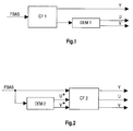
- Fig. 1 the arrangement of a conventional comb filter is shown.
- the FBAS signal FBAS is first fed to the comb filter CF1.
- This comb filter then splits the FBAS signal FBAS into a luminance signal Y and a chrominance signal that is still to be demodulated.
- the chrominance signal is then fed to a demodulator DEM1, in which the color difference signals U and V are regenerated.
- the algorithm selection is based only on an evaluation of the high-frequency signal components.
- the comb filter according to the invention is arranged as shown in FIG. 2.
- the FBAS signal FBAS is first fed to a demodulator DEM2.
- the color component signals U * and V * generated by this demodulator DEM2, like the FBAS signal FBAS, are then fed to the comb filter CF2.
- Comb filter CF2 then removes the carried chrominance signal components from the composite signal and removes the demodulated high-frequency luminance signals erroneously contained therein from color component signals U * and V *.
- the comb filter CF2 therefore processes demodulated chrominance signals in contrast to conventional comb filters.
- the separated luminance and color difference signals Y, U, V are then available at the output of the comb filter.
- FIG. 3 shows a block diagram of the comb filter CF2 according to the invention, a link of three lines being used as an example for the line comb filtering.
- the CVBS signal FBAS and the U * and V * signals are each delayed in two delay stages D1, D2 or D3, D4 or D5, D6.
- Line memories in particular FIFO memories, are preferably used for this.
- the differently delayed CVBS signals are then initially with a High-low-pass combination LHF1, LHF2 or LHF3 broken down into the respective high-pass component HPa, HPc, HPe and low-pass component LPa, LPc, LPe.
- Both the low-pass signals LPa, LPc, LPe and the demodulated chrominance signals Ua, Uc, Ue and Va, Vc, Ve of the differently delayed lines are then fed to a logic block FM.
- This block analyzes which patterns the signals have.
- the decision signals CM, LM, XC1 to XC5 are then assigned specific values and fed to the block DM.
- this block e.g. B. in table form, for the possible combinations of the decision signals, two decision values CD and LD are stored. The decision values are used to control the switching and averaging blocks for the luminance and chrominance signals.
- the low-frequency luminance component LPc is then added to the output signal of this block with the aid of an adder AL.
- blocks SC1 and SC2 are followed by averaging over several lines by means of a median filter M1 and M2, which can have line memories for delaying the color difference signals. This averaging eliminates switching artifacts that can be caused by noise in particular.
- FIG. 4 shows a block diagram of the logic block FM.
- the differently delayed lines are fed to the decision logic, different distance, difference and sum signals being calculated from the supplied signals. These values are then compared to preselected values or other calculated values. Different decision signals are then determined depending on the respective comparison result.
- a first distance value dac, dce or dae is determined for every two image lines, which corresponds to the distance between the color signals of the two lines given by the two color component signals U *, V *.
- These first distance values are then compared with preselected values or first distance values for another line combination or a fraction of these first distance values.
- block 4 it is checked whether the distance values dac, dce and dae are all smaller than a predetermined barrier with the value "15". If this is the case, the decision signal CM is assigned the value "0". If, on the other hand, at least one of the distance values lies above the predetermined barrier, the distance values are fed to the next comparison block 5. Depending on the structure of the chrominance signals, ie the result of the comparisons carried out by blocks 4 to 9, the decision signal CM thus has one of the values between "0" and "6".
- blocks 10 to 15 are used to make comparisons for difference values which result for the low-pass components of two picture lines each.
- a second decision signal LM is then assigned a value between "0" and "6", which reflects the structure in the luminance component of the examined image lines.
- further distance values are also determined in block 16.
- the distance values decs and dacs thus give the distance between the sum of the color signals of lines e and c or a and c from the origin. These distance values are compared with half the distance of the color signal of line c from the origin dc. It is also checked whether the distance from c to the origin dc is either less than a quarter of the distances da and de or greater than four times the distances da and de. Depending on these comparison results, the decision signals XC1, XC2 and XC3 are each assigned either the value "0" or "1".
- are used for the color component signals and (
- ) / 8 are calculated and again compared with one another or with a specific threshold value in order to give the decision signals XC4, XC5 a binary value assign.
- luminance and chrominance signals generally have different sampling frequencies (4: 1: 1).
- an adjustment could, for. B. done by performing a 4: 1 up-conversion of the chrominance signals before the comb filter.
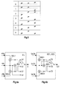
- the image signal modes corresponding to the decision signals CM and LM are illustrated in FIG. 5.
- mode 0 the values of all three lines are within a barrier and therefore close together.
- line e differs significantly from lines a and c, i.e. there is an edge. Accordingly, there is also an edge in mode 2, because line a differs significantly from lines c and e.
- mode 3 line a is between lines c and e, in mode 4 line e is between lines a and c.
- all lines are approximately in a line, in mode 6 in a zigzag.
- the result values CM, LM, XC1 - XC5 are evaluated in the block DM. It will be for every combination of the two Decision signals CM and LM decided how the chrominance signals and high-pass luminance signals are to be processed. For this purpose, the decision values CD and LD are determined, which are given in Tables 1 and 2, whereby for some CM / LM combinations two decision values are possible which depend on the current binary value of a further decision signal XC1 to XC5.
- the switching and averaging blocks SL and SC1, SC2 are controlled with the decision values CD and LD. Block diagrams of these two blocks are shown in Figures 6 a) and b).
- the high-frequency luminance signal components HPa, HPc, HPe of lines a, c and e are supplied to block SL.
- various combinations of the luminance signals are then calculated.
- These links are present at the outputs L1 - L4.
- a 0 signal is generated, ie only the low-pass luminance signal LPc is reproduced by the comb filter. This leads to a loss of sharpness, but it can completely eliminate ink residue that cannot be reduced by combining it with other lines.
- the block SC1 or SC2 from FIG. 6b is constructed in a very similar manner.
- the color component signals Ua, Va, Uc, Vc, Ue, Ve are present on the block and, by means of a link using the adders ASC1-ASC3, corresponding chrominance signals are available at the outputs C0-C3.
- the invention can be integrated in whole or in part in an integrated circuit, but can also be implemented in whole or in part by software.
- the invention can e.g. B. for PAL and NTSC television systems, but also for further developments of these systems. An application is particularly possible with PALplus receivers.
Landscapes
- Engineering & Computer Science (AREA)
- Multimedia (AREA)
- Signal Processing (AREA)
- Processing Of Color Television Signals (AREA)
Abstract
Description
Die Erfindung betrifft ein Verfahren und eine Schaltungsanordnung zum Trennen von Luminanz- und Chrominanzsignalen eines FBAS-Signals, insbesondere eine Kammfilter-Anordnung für PAL-Signale.The invention relates to a method and a circuit arrangement for separating luminance and chrominance signals of a CVBS signal, in particular a comb filter arrangement for PAL signals.
Bei analogen Farbfernseh-Übertragungsverfahren besteht das übertragene FBAS-Signal aus Luminanz- und Chrominanz-Signalen. Das Chrominanzsignal seinerseits setzt sich bei PAL und NTSC aus zwei Farbdifferenzsignalen zusammen (U/V-Signale bei PAL, I/Q-Signale bei NTSC), die in Quadraturphase auf einen Farbträger moduliert werden.In analog color television transmission methods, the transmitted CVBS signal consists of luminance and chrominance signals. In the case of PAL and NTSC, the chrominance signal in turn is composed of two color difference signals (U / V signals for PAL, I / Q signals for NTSC), which are modulated on a color carrier in the quadrature phase.
In einem Fernsehempfänger müssen die Luminanz- und Chrominanzsignale wieder voneinander getrennt werden, um eine separate Weiterverarbeitung zu ermöglichen. Hierfür werden Kammfilter eingesetzt, die auf der Basis von Zeilen-, Halbbild- und Bildverzögerungen zur Signaltrennung eine Verknüpfung von mehreren benachbarten Zeilen durchführen. Dabei ist es üblich, mit einer bildinhaltsabhängigen Steuerung zu arbeiten, die, je nachdem wie die Chrominanzsignale strukturiert sind, zwischen verschiedenen Filteralgorithmen umschaltet.In a television receiver, the luminance and chrominance signals must be separated from one another again in order to enable separate further processing. Comb filters are used for this purpose, which, on the basis of line, field and picture delays for signal separation, link several adjacent lines. It is customary to work with an image content-dependent control which, depending on how the chrominance signals are structured, switches between different filter algorithms.
Bei herkömmlichen Kammfiltern, die das FBAS-Signal in das Luminanzsignal und das aus den beiden noch zu demodulierenden Farbdifferenzsignalen bestehende Chrominanzsignal aufspalten, erfolgt insbesondere das Erkennen von Farbkanten nicht immer fehlerfrei. Dieses kann zu einer unvollständigen Trennung der Luminanz- und Chrominanzsignale führen, so daß Cross-Effekte häufig nicht völlig vermieden werden können.In the case of conventional comb filters which split the CVBS signal into the luminance signal and the chrominance signal which still consists of the two color difference signals still to be demodulated, the detection of color edges in particular is not always error-free. This can lead to an incomplete separation of the luminance and chrominance signals, so that cross effects can often not be completely avoided.
Der Erfindung liegt die Aufgabe zugrunde, ein Verfahren zum Trennen von Luminanz- und Chrominanzsignalen eines FBAS-Signals anzugeben, um insbesondere das Auftreten von Cross-Effekten, wie z. B. die als sogenannte "Hanging Dots" bekannten Kammfilterfehler, zu minimieren. Diese Aufgabe wird durch das in Anspruch 1 angegebene Verfahren gelöst.The invention has for its object to provide a method for separating luminance and chrominance signals of a composite signal, in particular to prevent the occurrence of cross effects, such as. B. to minimize the so-called "hanging dots" comb filter errors. This object is achieved by the method specified in
Der Erfindung liegt die weitere Aufgabe zugrunde, eine Schaltungsanordnung zum Trennen von Luminanz- und Chrominanzsignalen eines FBAS-Signals anzugeben. Diese Aufgabe wird durch die in Anspruch 6 angegebenene Schaltungsanordnung gelöst.The invention is based on the further object of specifying a circuit arrangement for separating luminance and chrominance signals of a CVBS signal. This object is achieved by the circuit arrangement specified in
Eine bessere Detektion von Farbkanten als bei bekannten Kammfiltern und damit eine verbesserte Trennung der Luminanz- und Chrominanzsignale kann erreicht werden, wenn zur Entscheidungsfindung der optimalen Zeilenverknüpfung, d.h. zur Auswahl des optimalen Filteralgorithmus, auch die Struktur des Luminanzsignales untersucht wird.A better detection of color edges than with known comb filters and thus an improved separation of the luminance and chrominance signals can be achieved if the optimal line combination, i.e. to select the optimal filter algorithm, the structure of the luminance signal is also examined.
Im Prinzip besteht daher das erfindungsgemäße Verfahren zum Trennen von Luminanz- und Chrominanzsignalen eines FBAS-Signals durch eine Verknüpfung von mehreren Bildzeilen, bei dem von verschiedenen Verknüpfungen eine Verknüpfung ausgewählt wird, darin, daß zunächst aus dem FBAS-Signal zwei Farbkomponentensignale demoduliert werden, die zusammen mit dem FBAS-Signal zur Bestimmung der auszuwählenden Verknüpfung ausgewertet werden und dann durch die ausgewählte Verknüpfung ein Luminanzsignal und Farbdifferenzsignale generiert werden.In principle, therefore, the method according to the invention for separating luminance and chrominance signals of a CVBS signal by linking several image lines, in which a link is selected from various links, is first to demodulate two color component signals from the CVBS signal are evaluated together with the CVBS signal to determine the link to be selected and then a luminance signal and color difference signals are generated by the selected link.
Vorteilhaft wird dabei nur der tieffrequente Anteil des FBAS-Signals ausgewertet, wobei die Farbkomponentensignale neben den Farbdifferenzsignalen noch den hochfrequenten Anteil der Luminanzsignale enthalten.Only the low-frequency component of the CVBS signal is advantageously evaluated, the color component signals in addition to the color difference signals also containing the high-frequency component of the luminance signals.
Vorzugsweise werden hierbei sowohl das FBAS-Signal als auch die Farbkomponentensignale jeweils um eine ganze Anzahl von Zeilen und um das Doppelte dieser Anzahl verzögert und aus dem hochfrequenten Anteil des FBAS-Signals sowie den Farbkomponentensignalen von drei nicht-, einfach- und doppeltverzögerten Zeilen durch eine Wichtung entsprechend der optimalen Verknüpfung die Chrominanzsignale sowie die hochfrequenten Luminanzsignale der einfachverzögerten Zeile generiert.Preferably, both the CVBS signal and the color component signals are each delayed by a whole number of lines and by twice this number, and the high-frequency component of the CVBS signal and the color component signals of three non-, single- and double-delayed lines are delayed by one Weighting according to the optimal link generates the chrominance signals as well as the high-frequency luminance signals of the single delay line.
Hierbei kann nach Generierung der Chrominanz- und hochfrequenten Luminanzsignale eine Mittelung der Chrominanzsignale über mehrere Zeilen durchgeführt werden und zu dem hochfrequenten Luminanzsignal der tieffrequente Anteil des einfachverzögerten FBAS-Signals addiert werden.After the chrominance and high-frequency luminance signals have been generated, the chrominance signals can be averaged over several lines and the low-frequency component of the single-delayed CVBS signal added to the high-frequency luminance signal.
Besonders vorteilhaft ist es hierbei, wenn
- a)
- in einer von den Farbkomponentensignalen aufgespannten komplexen Ebene für jeweils zwei Bildzeilen ein erster Abstandswert bestimmt wird, welcher dem Abstand der durch die beiden Farbkomponentensignale gegebenen Farbsignale der beiden Zeilen entspricht,
- diese ersten Abstandswerte mit vorgewählten Werten oder ersten Abstandswerten, die sich für eine andere Zeilenkombination ergeben, oder einem Bruchteil dieser ersten Abstandswerte verglichen wird, wobei auch mehrere Vergleiche gleichzeitig durchgeführt werden können,
- und in Abhängigkeit von dem Vergleichsergebnis entweder ersten Entscheidungssignalen ein bestimmter Wert zugewiesen wird oder ein weiterer Vergleich durchgeführt wird,
- b)
- für jeweils zwei Bildzeilen ein Differenzwert bestimmt wird, welcher dem Betrag der Differenz der tieffrequenten Anteile der FBAS-Signale der beiden Zeilen entspricht,
- dieser Differenzwert mit vorgewählten Werten oder Differenzwerten, die sich für eine andere Zeilenkombination ergeben, oder einem Bruchteil dieser Differenzwerte verglichen wird, wobei auch mehrere Vergleiche gleichzeitig durchgeführt werden können,
- und in Abhängigkeit von dem Vergleichsergebnis entweder zweiten Entscheidungssignalen ein bestimmter Wert zugewiesen wird oder ein weiterer Vergleich durchgeführt wird,
- c)
- in einer von den Farbkomponentensignalen aufgespannten komplexen Ebene ein zweiter und dritter Abstandswert bestimmt wird, wobei der zweite Abstandswert dem Abstand der Summe der durch die beiden Farbkomponentensignale gegebenen Farbsignale zweier Zeilen vom Ursprung und der dritte Abstandswert dem Abstand eines durch die beiden Farbkomponentensignale gegebenen Farbsignals einer Zeile vom Ursprung entspricht,
- zweite Abstandswerte mit dritten Abstandswerten oder einem Bruchteil dieser dritten Abstandswerte verglichen werden und dritte Abstandswerte einer Zeile mit dritten Abstandswerten einer anderen Zeile oder einem Bruchteil dieser dritten Abstandswerte verglichen werden, wobei auch mehrere Vergleiche gleichzeitig durchgeführt werden können,
- und in Abhängigkeit von den Vergleichsergebnissen zweiten Entscheidungssignalen jeweils ein Binärwert zugewiesen wird,
- d)
- für beide Farbkomponentensignale erste und zweite Summenwerte bestimmt werden, wobei der erste Summenwert dem Betrag der Summe von einem der beiden Farbkomponentensignale der mehreren Zeilen und der zweite Summenwert der Summe der Beträge von einem der beiden Farbkomponentensignale entspricht, wobei eine unterschiedliche Wichtung der Farbkomponentensignale der verschiedenen Zeilen vorgenommen werden kann
- erste Summenwerte mit zweiten Summenwerten oder einem Bruchteil dieser zweiten Summenwerte verglichen werden und erste Summenwerte beider Farbkomponenten mit einem bestimmten Wert verglichen werden, wobei auch mehrere Vergleiche gleichzeitig durchgeführt werden können,
- und in Abhängigkeit von den Vergleichsergebnissen dritten Entscheidungssignalen jeweils ein Binärwert zugewiesen wird.
- e)
und die Entscheidungssignale verwendet werden, um eine Verknüpfung auszuwählen.
- a)
- in a complex plane spanned by the color component signals, a first distance value is determined for every two image lines, which corresponds to the distance between the color signals of the two lines given by the two color component signals,
- these first distance values are compared with preselected values or first distance values which result for another line combination, or a fraction of these first distance values, it also being possible to carry out several comparisons at the same time,
- and depending on the comparison result, either a specific value is assigned to first decision signals or a further comparison is carried out,
- b)
- a difference value is determined for every two image lines, which corresponds to the amount of the difference between the low-frequency components of the CVBS signals of the two lines,
- this difference value with preselected values or difference values that result for another line combination, or a fraction of these difference values is compared, and several comparisons can also be carried out simultaneously,
- and depending on the comparison result, either a specific value is assigned to second decision signals or a further comparison is carried out,
- c)
- A second and third distance value is determined in a complex plane spanned by the color component signals, the second distance value being the distance between the sum of the color signals of two lines given by the two color component signals from the origin and the third distance value being the distance of a color signal of one line given by the two color component signals corresponds to the origin,
- second distance values are compared with third distance values or a fraction of these third distance values and third distance values of one line are compared with third distance values of another line or a fraction of these third distance values, wherein several comparisons can also be carried out simultaneously,
- and depending on the comparison results, second decision signals are each assigned a binary value,
- d)
- first and second sum values are determined for both color component signals, the first sum value corresponding to the amount of the sum of one of the two color component signals of the several lines and the second sum value corresponding to the sum of the amounts of one of the two color component signals, with a different weighting of the color component signals of the different lines can be made
- first sum values are compared with second sum values or a fraction of these second sum values and first sum values of both color components are compared with a certain value, it also being possible to carry out several comparisons at the same time,
- and, depending on the comparison results, third decision signals are each assigned a binary value.
- e)
and the decision signals are used to select a link.
Im Prinzip besteht die erfindungsgemäße Schaltungsanordnung darin, daß ein Demodulator vorgesehen ist, der aus dem FBAS-Signal zwei Farbkomponentensignale demoduliert, die zusammen mit dem FBAS-Signal einem Kammfilter zugeführt werden, in dem diese Signale zunächst zur Bestimmung der auszuwählenden Verknüpfung ausgewertet werden und dann durch die ausgewählte Verknüpfung ein Luminanzsignal und Farbdifferenzsignale generiert werden.In principle, the circuit arrangement according to the invention consists in that a demodulator is provided which demodulates two color component signals from the composite signal, which together with the composite signal are fed to a comb filter, in which these signals are first evaluated to determine the link to be selected and then a luminance signal and color difference signals are generated by the selected link.
Vorteilhaft sind hierbei im Kammfilter Zeilenspeicher vorgesehen, um sowohl das FBAS-Signal als auch die Farbkomponentensignale zu verzögern. Ferner werden die FBAS-und Farbkomponentensignale der unterschiedlich verzögerten Zeilen einer Entscheidungslogik und einem oder mehreren Schalt- und Mittelungsblöcken zugeführt, in denen die Chrominanzsignale sowie die hochfrequenten Luminanzsignale generiert werden.In this case, line memories are advantageously provided in the comb filter in order to delay both the CVBS signal and the color component signals. Furthermore, the CVBS and color component signals of the differently delayed lines are fed to a decision logic and one or more switching and averaging blocks, in which the chrominance signals and the high-frequency luminance signals are generated.
Vorzugsweise wird das dem Kammfilter zugeführte FBAS-Signal durch eine Hochpaß-Tiefpaß-Kombination in einen Hoch- und einen Tiefpaßanteil zerlegt und dem Schalt- und Mittelungsblock nur der Hochpaßanteil, der Entscheidungslogik nur der Tiefpaßanteil zugeführt.The CVBS signal fed to the comb filter is preferably broken down into a high and a low pass component by a high-pass / low-pass combination and only the high-pass component is fed to the switching and averaging block, and the low-pass component to the decision logic.
Ferner werden vorzugsweise zum einen die generierten Chrominanzsignale Medianfiltern zugeführt, die eine Mittelung der Chrominanzsignale über mehrere Zeilen durchführen, und zum anderen kann ein Addierer vorgesehen werden, um zu dem generierten hochfrequenten Luminanzsignal den tieffrequente Anteil des einfach verzögerten FBAS-Signals zu addieren.Furthermore, on the one hand, the generated chrominance signals are preferably supplied with median filters which average the chrominance signals over several lines, and on the other hand an adder can be provided in order to add the low-frequency component of the simply delayed CVBS signal to the generated high-frequency luminance signal.
Besonders vorteilhaft weist die Entscheidungslogik einen ersten Block auf, dem die unterschiedlich verzögerten Zeilen zugeführt werden, wobei aus den zugeführten Signalen verschiedene Abstands-, Differenz-, und Summensignale berechnet werden, diese Werte mit vorgewählten Werten oder anderen berechneten Werten verglichen werden und in Abhängigkeit von dem Vergleichsergebnis Entscheidungssignale bestimmt werden, und die Entscheidungssignale einem zweiten Block zugeführt werden, in dem für jede Kombination der Entscheidungssignale ein oder mehrere Entscheidungswerte bestimmt werden, die dem oder den Schalt- und Mittelungsblöcken zur Ansteuerung zugeführt werden.Particularly advantageously, the decision logic has a first block, to which the differently delayed lines are fed, different distance, difference and sum signals being calculated from the supplied signals, these values being compared with preselected values or other calculated values and depending on decision signals are determined from the comparison result, and the decision signals are fed to a second block in which, for each combination of the decision signals, one or more decision values are determined which are fed to the switching and averaging blocks for actuation.
Anhand der Zeichnungen werden Ausführungsbeispiele der Erfindung beschrieben. Diese zeigen in:
- Fig. 1
- die Anordnung eines herkömmlichen Kammfilters und PAL-Demodulators,
- Fig. 2
- die Anordnung des erfindungsgemäßen Kammfilters,
- Fig. 3
- ein Blockschaltbild des erfindungsgemäßen Kammfilters,
- Fig. 4
- ein Blockschaltbild des Logik-Blocks aus Fig. 3,
- Fig. 5
- verschiedene mögliche Anordnungen der Zeilen,
- Fig. 6
- ein Blockschaltbild des Schalt- und Mittelungsblocks für a) die Luminanzsignale, b) die Chrominanzsignale.
- Fig. 1
- the arrangement of a conventional comb filter and PAL demodulator,
- Fig. 2
- the arrangement of the comb filter according to the invention,
- Fig. 3
- 2 shows a block diagram of the comb filter according to the invention,
- Fig. 4
- 3 shows a block diagram of the logic block from FIG. 3,
- Fig. 5
- different possible arrangements of the lines,
- Fig. 6
- a block diagram of the switching and averaging block for a) the luminance signals, b) the chrominance signals.
In Fig. 1 ist die Anordnung eines herkömmlichen Kammfilters dargestellt. Das FBAS-Signal FBAS wird erst dem Kammfilter CF1 zugeführt. Durch dieses Kammfilter wird dann das FBAS-Signal FBAS in ein Luminanzsignal Y und ein noch zu demodulierendes Chrominanzsignal aufgespaltet. Das Chrominanzsignal wird dann einem Demodulator DEM1 zugeführt, in dem die Farbdifferenzsignale U und V regeneriert werden. Die Algorithmusauswahl beruht hierbei lediglich auf einer Auswertung der hochfrequenten Signalanteile.In Fig. 1 the arrangement of a conventional comb filter is shown. The FBAS signal FBAS is first fed to the comb filter CF1. This comb filter then splits the FBAS signal FBAS into a luminance signal Y and a chrominance signal that is still to be demodulated. The chrominance signal is then fed to a demodulator DEM1, in which the color difference signals U and V are regenerated. The algorithm selection is based only on an evaluation of the high-frequency signal components.
Das erfindungsgemäße Kammfilter wird dagegen, wie in Fig. 2 dargestellt, angeordnet. Das FBAS-Signal FBAS wird zunächst einem Demodulator DEM2 zugeführt. Die von diesem Demodulator DEM2 erzeugten Farbkomponentensignale U* und V* werden dann ebenso wie das FBAS-Signal FBAS dem Kammfilter CF2 zugeführt. Durch das Kammfilter CF2 werden dann aus dem FBAS-Signal die geträgerten Chrominanzsignal-Anteile entfernt und aus den Farbkomponentensignalen U* und V* die dort fälschlicherweise enthaltenen demodulierten hochfrequenten Luminanzsignale entfernt. Das Kammfilter CF2 verarbeitet daher im Gegensatz zu herkömmlichen Kammfiltern demodulierte Chrominanzsignale. Am Ausgang des Kammfilters stehen dann die separierten Luminanz- und Farbdifferenzsignale Y, U, V zur Verfügung.In contrast, the comb filter according to the invention is arranged as shown in FIG. 2. The FBAS signal FBAS is first fed to a demodulator DEM2. The color component signals U * and V * generated by this demodulator DEM2, like the FBAS signal FBAS, are then fed to the comb filter CF2. Comb filter CF2 then removes the carried chrominance signal components from the composite signal and removes the demodulated high-frequency luminance signals erroneously contained therein from color component signals U * and V *. The comb filter CF2 therefore processes demodulated chrominance signals in contrast to conventional comb filters. The separated luminance and color difference signals Y, U, V are then available at the output of the comb filter.
In Fig. 3 ist ein Blockschaltbild des erfindungsgemäßen Kammfilters CF2 dargestellt, wobei exemplarisch für die Zeilen-Kammfilterung eine Verknüpfung von jeweils drei Zeilen erfolgt. Für diesen Fall werden sowohl das FBAS-Signal FBAS als auch die U*- und V*-Signale jeweils in zwei Verzögerungsstufen D1, D2 bzw. D3, D4 oder D5, D6 verzögert. Hierfür werden vorzugsweise Zeilenspeicher, insbesondere FIFO-Speicher, verwendet. Für PAL-Signale erfolgt jeweils eine Verzögerung um zwei Zeilen, für NTSC-Signale jeweils eine Verzögerung um eine Zeile. Die unterschiedlich verzögerten FBAS-Signale werden dann zunächst mit einer Hoch-Tiefpaß-Kombination LHF1, LHF2 oder LHF3 in den jeweiligen Hochpaßanteil HPa, HPc, HPe und Tiefpaßanteil LPa, LPc, LPe zerlegt. Sowohl die Tiefpaßsignale LPa, LPc, LPe, als auch die demodulierten Chrominanzsignale Ua, Uc, Ue bzw. Va, Vc, Ve der unterschiedlich verzögerten Zeilen werden dann einem Logik-Block FM zugeführt. In diesem Block wird analysiert, welche Muster die Signale aufweisen. Je nach erkannter Struktur werden dann den Entscheidungssignalen CM, LM, XC1 bis XC5 bestimmte Werte zugewiesen und dem Block DM zugeführt. In diesem Block sind, z. B. in Tabellenform, für die möglichen Kombinationen der Entscheidungssignale jeweils zwei Entscheidungswerte CD und LD abgelegt. Die Entscheidungswerte dienen hierbei zur Ansteuerung der Schalt- und Mittelungsblöcke für die Luminanz- und Chrominanzsignale. Da von den Luminanzsignalen durch den Schalt- und Mittelungsblock SL nur die jeweiligen Hochpaß-Signale verarbeitet werden, wird zu dem Ausgangssignal dieses Blocks mit Hilfe eines Addierers AL anschließend der tieffrequente Luminanzanteil LPc hinzuaddiert. Bei den Farbdifferenzsignalen folgt im Anschluß an die Blöcke SC1 bzw. SC2 jeweils noch eine Mittelung über mehrere Zeilen mittels eines Medianfilters M1 bzw. M2, der zur Verzögerung der Farbdifferenzsignale Zeilenspeicher aufweisen kann. Mit Hilfe dieser Mittelung werden Schaltartefakte, die insbesondere durch Rauschen verursacht werden können, eliminiert.FIG. 3 shows a block diagram of the comb filter CF2 according to the invention, a link of three lines being used as an example for the line comb filtering. In this case, the CVBS signal FBAS and the U * and V * signals are each delayed in two delay stages D1, D2 or D3, D4 or D5, D6. Line memories, in particular FIFO memories, are preferably used for this. There is a two-line delay for PAL signals and a one-line delay for NTSC signals. The differently delayed CVBS signals are then initially with a High-low-pass combination LHF1, LHF2 or LHF3 broken down into the respective high-pass component HPa, HPc, HPe and low-pass component LPa, LPc, LPe. Both the low-pass signals LPa, LPc, LPe and the demodulated chrominance signals Ua, Uc, Ue and Va, Vc, Ve of the differently delayed lines are then fed to a logic block FM. This block analyzes which patterns the signals have. Depending on the structure identified, the decision signals CM, LM, XC1 to XC5 are then assigned specific values and fed to the block DM. In this block, e.g. B. in table form, for the possible combinations of the decision signals, two decision values CD and LD are stored. The decision values are used to control the switching and averaging blocks for the luminance and chrominance signals. Since only the respective high-pass signals are processed by the switching and averaging block SL of the luminance signals, the low-frequency luminance component LPc is then added to the output signal of this block with the aid of an adder AL. In the case of the color difference signals, blocks SC1 and SC2 are followed by averaging over several lines by means of a median filter M1 and M2, which can have line memories for delaying the color difference signals. This averaging eliminates switching artifacts that can be caused by noise in particular.
In Fig. 4 ist ein Blockschaltbild des Logik-Blocks FM dargestellt. Der Entscheidungslogik werden die unterschiedlich verzögerten Zeilen zugeführt, wobei aus den zugeführten Signalen verschiedene Abstands-, Differenz-, und Summensignale berechnet werden. Diese Werte werden dann mit vorgewählten Werten oder anderen berechneten Werten verglichen. In Abhängigkeit von dem jeweiligen Vergleichsergebnis werden dann verschiedene Entscheidungssignale bestimmt.4 shows a block diagram of the logic block FM. The differently delayed lines are fed to the decision logic, different distance, difference and sum signals being calculated from the supplied signals. These values are then compared to preselected values or other calculated values. Different decision signals are then determined depending on the respective comparison result.
Die Berechnung der verschiedenen Abstands-, Differenz-, und Summensignale wird im folgenden detaillierter beschrieben.The calculation of the various distance, difference, and sum signals is described in more detail below.
In einer von den Farbkomponentensignalen aufgespannten komplexen Ebene wird für jeweils zwei Bildzeilen ein erster Abstandswert dac, dce oder dae bestimmt, welcher dem Abstand der durch die beiden Farbkomponentensignale U*, V* gegebenen Farbsignale der beiden Zeilen entspricht. So wird in dem Block 1 der Abstandswert dac für die beiden Zeilen a und c bestimmt, und ergibt sich z.B. mit Hilfe des Satzes von Phytagoras zu ![]()
![]()
Entsprechend werden in den Blöcken 10 bis 15 Vergleiche für Differenzwerte durchgeführt, die sich für die Tiefpaß-Anteile von jeweils zwei Bildzeilen ergeben. In Abhängigkeit von dem Vergleichsergebnis wird dann einem zweiten Entscheidungssignal LM ein Wert zwischen "0" und "6" zugewiesen, der die Struktur im Luminanzanteil der untersuchten Bildzeilen wiederspiegelt.Correspondingly, blocks 10 to 15 are used to make comparisons for difference values which result for the low-pass components of two picture lines each. Depending on the comparison result, a second decision signal LM is then assigned a value between "0" and "6", which reflects the structure in the luminance component of the examined image lines.
Für das Erkennen von Cross-Colour-Störungen in verschiedenen Sonderfällen werden ferner im Block 16 noch weitere Abstandswerte bestimmt. So geben die Abstandswerte decs und dacs den Abstand der Summe der Farbsignale der Zeilen e und c bzw. a und c vom Ursprung an. Diese Abstandswerte werden mit dem halben Abstand des Farbsignals der Zeile c vom Ursprung dc verglichen. Ferner wird überprüft, ob der Abstand von c zum Ursprung dc entweder kleiner als ein Viertel der Abstände da und de oder größer als das Vierfache der Abstände da und de ist. In Abhängigkeit von diesen Vergleichsergebnissen werden den Entscheidungssignalen XC1, XC2 und XC3 jeweils entweder der Wert "0" oder "1" zugewiesen.For the detection of cross-color disturbances in various special cases, further distance values are also determined in
Ferner werden für die Farbkomponentensignale die Werte |Ua,Va+2*Uc,Vc+Ue,Ve| und (|Ua,Va|+2*|Uc,Vc|+|Ue,Ve|)/8 berechnet und wiederum miteinander oder mit einem bestimmten Schwellwert verglichen, um den Entscheidungssignalen XC4, XC5 jeweils einen Binärwert zuzuweisen.Furthermore, the values | U a , V a + 2 * U c , V c + U e , V e | are used for the color component signals and (| U a , V a | + 2 * | U c , V c | + | U e , V e |) / 8 are calculated and again compared with one another or with a specific threshold value in order to give the decision signals XC4, XC5 a binary value assign.
Es ist zu beachten, daß in dem Blockschaltbild das Verfahren zwar so dargestellt ist, als ob alle Signale mit der gleichen Abtastfrequenz vorliegen würden, Luminanz- und Chrominanzsignale im allgemeinen jedoch verschiedene Abtastfrequenzen (4:1:1) haben. Eine Anpassung könnte jedoch z. B. dadurch erfolgen, daß vor dem Kammfilter eine 4:1-Aufwärts-Konversion der Chrominanzsignale durchgeführt wird.It should be noted that although the method is shown in the block diagram as if all signals were present with the same sampling frequency, luminance and chrominance signals generally have different sampling frequencies (4: 1: 1). However, an adjustment could, for. B. done by performing a 4: 1 up-conversion of the chrominance signals before the comb filter.
Die den Entscheidungssignalen CM und LM entsprechenden Bildsignal-Modi sind in Fig. 5 veranschaulicht. Für den Mode 0 liegen die Werte aller drei Zeilen innerhalb einer Schranke und damit dicht beieinander. Liegt der Mode 1 vor, so unterscheidet sich die Zeile e deutlich von den Zeilen a und c, es liegt also eine Kante vor. Entsprechend liegt auch bei Mode 2 eine Kante vor, denn Zeile a unterscheidet sich deutlich von den Zeilen c und e. Bei Mode 3 liegt die Zeile a zwischen den Zeilen c und e, bei Mode 4 die Zeile e zwischen den Zeilen a und c. Bei Mode 5 schließlich liegen alle Zeilen etwa in einer Linie, bei Mode 6 im Zickzack.The image signal modes corresponding to the decision signals CM and LM are illustrated in FIG. 5. For
Die Ergebniswerte CM, LM, XC1 - XC5 werden in dem Block DM ausgewertet. Es wird für jede Kombination der beiden Entscheidungssignale CM und LM entschieden, wie die Chrominanzsignale bzw. Hochpaß-Luminanzsignale verarbeitet werden sollen. Hierfür werden die Entscheidungswerte CD bzw. LD bestimmt, die in den Tabellen 1 bzw. 2 angegeben sind, wobei für manche CM/LM-Kombinationen zwei Entscheidungswerte möglich sind, die von dem aktuellen Binärwert eines weiteren Entscheidungssignals XC1 bis XC5 abhängen.

Mit den Entscheidungswerten CD bzw. LD werden die Schalt- und Mittelungsblöcke SL bzw. SC1, SC2 angesteuert. Blockschaltbilder dieser beiden Blöcke sind in den Abbildungen 6 a) bzw. b) wiedergegeben. Dem Block SL werden jeweils die hochfrequenten Luminanzsignalanteile HPa, HPc, HPe der Zeilen a, c und e zugeführt. Mit Hilfe der Addierer ASL1 - ASL3 werden dann verschiedene Verknüpfungen der Luminanzsignale berechnet. Diese Verknüpfungen liegen an den Ausgängen L1 - L4 an, so ergibt sich z. B. für L2 ein Ausgangswert HPe + HPc. Bei Verwendung des Ausgangs L0 wird ein 0-Signal erzeugt, d. h. nur das Tiefpaß-Luminanzsignal LPc wird durch den Kammfilter wiedergegeben. Dieses führt dann zwar zu einem Schärfeverlust, jedoch können damit Farbträgerreste, die durch Kombination mit anderen Zeilen nicht reduziert werden können, komplett eliminiert werden.The switching and averaging blocks SL and SC1, SC2 are controlled with the decision values CD and LD. Block diagrams of these two blocks are shown in Figures 6 a) and b). The high-frequency luminance signal components HPa, HPc, HPe of lines a, c and e are supplied to block SL. With the help of the adders ASL1 - ASL3, various combinations of the luminance signals are then calculated. These links are present at the outputs L1 - L4. B. for L2 Baseline HPe + HPc. When the output L0 is used, a 0 signal is generated, ie only the low-pass luminance signal LPc is reproduced by the comb filter. This leads to a loss of sharpness, but it can completely eliminate ink residue that cannot be reduced by combining it with other lines.
Sehr ähnlich ist auch der Block SC1 bzw. SC2 aus Fig. 6b aufgebaut. Hierbei liegen die Farbkomponentensignale Ua, Va, Uc, Vc, Ue, Ve an dem Block an und durch eine Verknüpfung mit Hilfe der Addierer ASC1 - ASC3 stehen entsprechende Chrominanzsignale an den Ausgängen C0 - C3 zur Verfügung.The block SC1 or SC2 from FIG. 6b is constructed in a very similar manner. The color component signals Ua, Va, Uc, Vc, Ue, Ve are present on the block and, by means of a link using the adders ASC1-ASC3, corresponding chrominance signals are available at the outputs C0-C3.
Die Erfindung kann ganz oder teilweise in einen Integrierten Schaltkreis integriert werden, jedoch ebenso auch ganz oder teilweise durch Software realisiert werden.The invention can be integrated in whole or in part in an integrated circuit, but can also be implemented in whole or in part by software.
Die Erfindung kann z. B. für PAL- und NTSC-Fernsehsysteme, aber auch für Weiterentwicklungen dieser Systeme genutzt werden. Eine Anwendung ist insbesondere auch bei PALplus-Empfängern möglich.The invention can e.g. B. for PAL and NTSC television systems, but also for further developments of these systems. An application is particularly possible with PALplus receivers.
Claims (10)
und die Entscheidungssignale (CM, LM, XC1 - XC5) verwendet werden, um eine Verknüpfung auszuwählen.
and the decision signals (CM, LM, XC1 - XC5) are used to select a link.
Applications Claiming Priority (2)
| Application Number | Priority Date | Filing Date | Title |
|---|---|---|---|
| DE19609193A DE19609193A1 (en) | 1996-03-09 | 1996-03-09 | Method and circuit arrangement for separating luminance and chrominance signals of a CVBS signal |
| DE19609193 | 1996-03-09 |
Publications (3)
| Publication Number | Publication Date |
|---|---|
| EP0794677A2 true EP0794677A2 (en) | 1997-09-10 |
| EP0794677A3 EP0794677A3 (en) | 1997-09-24 |
| EP0794677B1 EP0794677B1 (en) | 2004-04-21 |
Family
ID=7787739
Family Applications (1)
| Application Number | Title | Priority Date | Filing Date |
|---|---|---|---|
| EP97103172A Expired - Lifetime EP0794677B1 (en) | 1996-03-09 | 1997-02-27 | Method and circuit arrangement for separating luminance and chrominance signals from a composite colour signal |
Country Status (5)
| Country | Link |
|---|---|
| US (1) | US5973753A (en) |
| EP (1) | EP0794677B1 (en) |
| JP (1) | JPH09331545A (en) |
| CN (1) | CN1112054C (en) |
| DE (2) | DE19609193A1 (en) |
Families Citing this family (9)
| Publication number | Priority date | Publication date | Assignee | Title |
|---|---|---|---|---|
| JP2000069502A (en) * | 1998-08-24 | 2000-03-03 | Sony Corp | Video signal processing circuit and image pickup device using it |
| US6771321B2 (en) * | 2001-11-06 | 2004-08-03 | Broadcom Corporation | Method and system for performing PAL luma two line vertical combing |
| CN100477807C (en) * | 2004-01-17 | 2009-04-08 | 深圳创维-Rgb电子有限公司 | High-definition super processor and method therefor |
| CN100486342C (en) * | 2004-09-09 | 2009-05-06 | 凌阳科技股份有限公司 | Three-dimensional video hybrid signal demodulation method and system capable of suppressing false color noise |
| KR100688519B1 (en) * | 2005-01-13 | 2007-03-02 | 삼성전자주식회사 | Digital Image Signal Processing Apparatus and Method for Field-based Adaptive Spatiotemporal |
| KR100674939B1 (en) * | 2005-01-13 | 2007-01-26 | 삼성전자주식회사 | Digital Image Signal Processing Apparatus and Method for Frame-based Adaptive Spatio-temporal Y / C Separation |
| CN101340597B (en) * | 2007-07-06 | 2010-12-15 | 晨星半导体股份有限公司 | Image processing method and image processing device |
| US8238443B2 (en) * | 2008-01-12 | 2012-08-07 | Huaya Microelectronics | Digital timing extraction and recovery in a digital video decoder |
| CN102026004B (en) * | 2009-09-10 | 2013-01-30 | 联咏科技股份有限公司 | Image color processing element and method |
Citations (2)
| Publication number | Priority date | Publication date | Assignee | Title |
|---|---|---|---|---|
| EP0590831A2 (en) * | 1992-09-30 | 1994-04-06 | Sony Corporation | Luminance and chrominance signal separation circuits |
| US5424784A (en) * | 1994-09-06 | 1995-06-13 | Raytheon Company | Method and apparatus for cross fading between combed and simple filtered outputs |
Family Cites Families (13)
| Publication number | Priority date | Publication date | Assignee | Title |
|---|---|---|---|---|
| US3591707A (en) * | 1969-01-08 | 1971-07-06 | Gen Electric | Color television demodulator |
| US3946431A (en) * | 1974-10-01 | 1976-03-23 | Basf Aktiengesellschaft | Synchronized demodulation of the chrominance signal with switched carrier phase angles |
| JPS5760791A (en) * | 1980-09-30 | 1982-04-12 | Toshiba Corp | Demodulating circuit for wide-band receiving chrominance |
| US4573068A (en) * | 1984-03-21 | 1986-02-25 | Rca Corporation | Video signal processor for progressive scanning |
| GB8509306D0 (en) * | 1985-04-11 | 1985-05-15 | British Broadcasting Corp | Pal decoders |
| US4893176A (en) * | 1985-10-09 | 1990-01-09 | Faroudja Y C | Adaptive comb filter for quadrature modulated color television systems |
| GB8622680D0 (en) * | 1986-09-19 | 1986-10-22 | Robinson R N | Decoder |
| GB2223142B (en) * | 1988-09-23 | 1993-01-06 | Sony Corp | Separating components of composite digital video signals |
| DE3931903C2 (en) * | 1989-09-25 | 1994-10-27 | Broadcast Television Syst | Method and circuit for signal separation of a PAL signal |
| EP0613311A1 (en) * | 1993-02-26 | 1994-08-31 | Kabushiki Kaisha Toshiba | Y/C separating circuit |
| US5347321A (en) * | 1993-09-30 | 1994-09-13 | Texas Instruments Incorporated | Color separator for digital television |
| KR0157480B1 (en) * | 1994-06-18 | 1998-11-16 | 김광호 | Luminance and Color Signal Separation Methods and Circuits Adapting to the Edge Direction in Image Processing |
| JPH0998291A (en) * | 1995-07-26 | 1997-04-08 | Nec Eng Ltd | Automatic sampling device |
-
1996
- 1996-03-09 DE DE19609193A patent/DE19609193A1/en not_active Withdrawn
-
1997
- 1997-02-10 US US08/797,913 patent/US5973753A/en not_active Expired - Lifetime
- 1997-02-27 EP EP97103172A patent/EP0794677B1/en not_active Expired - Lifetime
- 1997-02-27 DE DE59711526T patent/DE59711526D1/en not_active Expired - Lifetime
- 1997-02-27 CN CN97103405A patent/CN1112054C/en not_active Expired - Fee Related
- 1997-03-06 JP JP9051869A patent/JPH09331545A/en active Pending
Patent Citations (2)
| Publication number | Priority date | Publication date | Assignee | Title |
|---|---|---|---|---|
| EP0590831A2 (en) * | 1992-09-30 | 1994-04-06 | Sony Corporation | Luminance and chrominance signal separation circuits |
| US5424784A (en) * | 1994-09-06 | 1995-06-13 | Raytheon Company | Method and apparatus for cross fading between combed and simple filtered outputs |
Non-Patent Citations (2)
| Title |
|---|
| IEEE TRANSACTIONS ON CONSUMER ELECTRONICS, Bd. 35, Nr. 3, 1.August 1989, Seiten 259-265, XP000065819 ATSUSHI ISHIZU ET AL: "DIGITAL SIGNAL PROCESSING FOR IMPROVED NTSC TELEVISION RECEIVER" * |
| MASAHIKO ACHIHA ET AL: "MOTION-ADAPTIVE ENHANCED DECODER AND UP-CONVERTER FOR PAL SIGNALS" 13.Juni 1991 , BROADCAST SESSIONS, MONTREUX, JUNE 13 - 18, 1991, VOL. -, NR. -, PAGE(S) 197 - 208 , CCITT XP000268889 * Seite 206; Abbildungen 17,18 * * |
Also Published As
| Publication number | Publication date |
|---|---|
| CN1164804A (en) | 1997-11-12 |
| EP0794677A3 (en) | 1997-09-24 |
| EP0794677B1 (en) | 2004-04-21 |
| DE59711526D1 (en) | 2004-05-27 |
| US5973753A (en) | 1999-10-26 |
| JPH09331545A (en) | 1997-12-22 |
| CN1112054C (en) | 2003-06-18 |
| DE19609193A1 (en) | 1997-09-11 |
Similar Documents
| Publication | Publication Date | Title |
|---|---|---|
| DE69622614T2 (en) | Adaptive error diffusion method | |
| DE69603268T2 (en) | LUMINANCE / CHROMINANCE SEPARATING FILTER WITH COMMON DELAY ELEMENT | |
| DE3226038C2 (en) | Filter circuit | |
| DE2810697C2 (en) | Method for separating the chrominance signal from the luminance signal in colour television signals with quadrature-modulated colour subcarriers | |
| DE3784769T2 (en) | VIDEO SIGNAL PROCESSING CIRCUITS. | |
| DE3842977C2 (en) | Mixing device for video signals | |
| DE3821398C2 (en) | Method and device for separating luminance and color signals of a color television signal mixture | |
| DE3234938C2 (en) | ||
| DE4039558C2 (en) | Brightness signal / color signal switch for a color television signal | |
| EP0344579B1 (en) | Device for reducing noise and cross-colour in television signals | |
| EP0794677B1 (en) | Method and circuit arrangement for separating luminance and chrominance signals from a composite colour signal | |
| DE69928576T2 (en) | Luminance and chrominance isolation circuit | |
| DE69405276T2 (en) | Comb filter to reduce cross color phenomena and noise | |
| DE3842978C2 (en) | Mixing device for video signals | |
| DE3786581T2 (en) | ENCODING AND DECODING DIGITAL VIDEO COMPONENT SIGNALS. | |
| DE4124698C2 (en) | ||
| DE69026441T2 (en) | Adaptive comb filter and method for separating video signal components | |
| DE69323947T2 (en) | Luminance / chrominance signal separation circuits | |
| DE19523438A1 (en) | Method for superimposing a background image signal into parts of a foreground image signal and circuit for carrying out this method | |
| DE3152649C2 (en) | ||
| DE3878741T2 (en) | RECOVERY OF THE LUMINANCE AND CHROMINANCE INFORMATION OF A CODED COLOR TELEVISION SIGNAL. | |
| DE4142782A1 (en) | VARIABLE CHROMINANCE FILTERING FOR ENCODING TV SIGNALS | |
| DE69714638T2 (en) | 2-line Y / C separation circuit | |
| DE3639733A1 (en) | ARRANGEMENT FOR IMPROVING VERTICAL IMAGE UNITS FOR A VIDEO PLAYBACK SYSTEM | |
| DE68908911T2 (en) | Circuit for separating the brightness signal from a color signal. |
Legal Events
| Date | Code | Title | Description |
|---|---|---|---|
| PUAI | Public reference made under article 153(3) epc to a published international application that has entered the european phase |
Free format text: ORIGINAL CODE: 0009012 |
|
| PUAL | Search report despatched |
Free format text: ORIGINAL CODE: 0009013 |
|
| AK | Designated contracting states |
Kind code of ref document: A2 Designated state(s): DE FR GB IT |
|
| AK | Designated contracting states |
Kind code of ref document: A3 Designated state(s): DE FR GB IT |
|
| 17P | Request for examination filed |
Effective date: 19980221 |
|
| 17Q | First examination report despatched |
Effective date: 20020618 |
|
| GRAP | Despatch of communication of intention to grant a patent |
Free format text: ORIGINAL CODE: EPIDOSNIGR1 |
|
| GRAS | Grant fee paid |
Free format text: ORIGINAL CODE: EPIDOSNIGR3 |
|
| GRAA | (expected) grant |
Free format text: ORIGINAL CODE: 0009210 |
|
| AK | Designated contracting states |
Kind code of ref document: B1 Designated state(s): DE FR GB IT |
|
| REG | Reference to a national code |
Ref country code: GB Ref legal event code: FG4D Free format text: NOT ENGLISH |
|
| GBT | Gb: translation of ep patent filed (gb section 77(6)(a)/1977) |
Effective date: 20040421 |
|
| REF | Corresponds to: |
Ref document number: 59711526 Country of ref document: DE Date of ref document: 20040527 Kind code of ref document: P |
|
| ET | Fr: translation filed | ||
| PLBE | No opposition filed within time limit |
Free format text: ORIGINAL CODE: 0009261 |
|
| STAA | Information on the status of an ep patent application or granted ep patent |
Free format text: STATUS: NO OPPOSITION FILED WITHIN TIME LIMIT |
|
| REG | Reference to a national code |
Ref country code: FR Ref legal event code: D6 |
|
| 26N | No opposition filed |
Effective date: 20050124 |
|
| PGFP | Annual fee paid to national office [announced via postgrant information from national office to epo] |
Ref country code: FR Payment date: 20110310 Year of fee payment: 15 Ref country code: IT Payment date: 20110219 Year of fee payment: 15 Ref country code: DE Payment date: 20110217 Year of fee payment: 15 |
|
| PGFP | Annual fee paid to national office [announced via postgrant information from national office to epo] |
Ref country code: GB Payment date: 20110225 Year of fee payment: 15 |
|
| GBPC | Gb: european patent ceased through non-payment of renewal fee |
Effective date: 20120227 |
|
| REG | Reference to a national code |
Ref country code: FR Ref legal event code: ST Effective date: 20121031 |
|
| PG25 | Lapsed in a contracting state [announced via postgrant information from national office to epo] |
Ref country code: IT Free format text: LAPSE BECAUSE OF NON-PAYMENT OF DUE FEES Effective date: 20120227 |
|
| REG | Reference to a national code |
Ref country code: DE Ref legal event code: R119 Ref document number: 59711526 Country of ref document: DE Effective date: 20120901 |
|
| PG25 | Lapsed in a contracting state [announced via postgrant information from national office to epo] |
Ref country code: GB Free format text: LAPSE BECAUSE OF NON-PAYMENT OF DUE FEES Effective date: 20120227 Ref country code: FR Free format text: LAPSE BECAUSE OF NON-PAYMENT OF DUE FEES Effective date: 20120229 |
|
| PG25 | Lapsed in a contracting state [announced via postgrant information from national office to epo] |
Ref country code: DE Free format text: LAPSE BECAUSE OF NON-PAYMENT OF DUE FEES Effective date: 20120901 |