EP0791955B1 - Integrated circuit interconnections - Google Patents
Integrated circuit interconnections Download PDFInfo
- Publication number
- EP0791955B1 EP0791955B1 EP97102764A EP97102764A EP0791955B1 EP 0791955 B1 EP0791955 B1 EP 0791955B1 EP 97102764 A EP97102764 A EP 97102764A EP 97102764 A EP97102764 A EP 97102764A EP 0791955 B1 EP0791955 B1 EP 0791955B1
- Authority
- EP
- European Patent Office
- Prior art keywords
- capillary tube
- wire
- vibrating
- cone angle
- capillary
- Prior art date
- Legal status (The legal status is an assumption and is not a legal conclusion. Google has not performed a legal analysis and makes no representation as to the accuracy of the status listed.)
- Expired - Lifetime
Links
Images

Classifications
-
- B—PERFORMING OPERATIONS; TRANSPORTING
- B23—MACHINE TOOLS; METAL-WORKING NOT OTHERWISE PROVIDED FOR
- B23K—SOLDERING OR UNSOLDERING; WELDING; CLADDING OR PLATING BY SOLDERING OR WELDING; CUTTING BY APPLYING HEAT LOCALLY, e.g. FLAME CUTTING; WORKING BY LASER BEAM
- B23K20/00—Non-electric welding by applying impact or other pressure, with or without the application of heat, e.g. cladding or plating
- B23K20/002—Non-electric welding by applying impact or other pressure, with or without the application of heat, e.g. cladding or plating specially adapted for particular articles or work
- B23K20/004—Wire welding
- B23K20/005—Capillary welding
- B23K20/007—Ball bonding
-
- B—PERFORMING OPERATIONS; TRANSPORTING
- B23—MACHINE TOOLS; METAL-WORKING NOT OTHERWISE PROVIDED FOR
- B23K—SOLDERING OR UNSOLDERING; WELDING; CLADDING OR PLATING BY SOLDERING OR WELDING; CUTTING BY APPLYING HEAT LOCALLY, e.g. FLAME CUTTING; WORKING BY LASER BEAM
- B23K2101/00—Articles made by soldering, welding or cutting
- B23K2101/36—Electric or electronic devices
- B23K2101/40—Semiconductor devices
-
- H—ELECTRICITY
- H10—SEMICONDUCTOR DEVICES; ELECTRIC SOLID-STATE DEVICES NOT OTHERWISE PROVIDED FOR
- H10W—GENERIC PACKAGES, INTERCONNECTIONS, CONNECTORS OR OTHER CONSTRUCTIONAL DETAILS OF DEVICES COVERED BY CLASS H10
- H10W72/00—Interconnections or connectors in packages
- H10W72/071—Connecting or disconnecting
- H10W72/0711—Apparatus therefor
- H10W72/07118—Means for cleaning, e.g. brushes
-
- H—ELECTRICITY
- H10—SEMICONDUCTOR DEVICES; ELECTRIC SOLID-STATE DEVICES NOT OTHERWISE PROVIDED FOR
- H10W—GENERIC PACKAGES, INTERCONNECTIONS, CONNECTORS OR OTHER CONSTRUCTIONAL DETAILS OF DEVICES COVERED BY CLASS H10
- H10W72/00—Interconnections or connectors in packages
- H10W72/071—Connecting or disconnecting
- H10W72/0711—Apparatus therefor
- H10W72/07141—Means for applying energy, e.g. ovens or lasers
-
- H—ELECTRICITY
- H10—SEMICONDUCTOR DEVICES; ELECTRIC SOLID-STATE DEVICES NOT OTHERWISE PROVIDED FOR
- H10W—GENERIC PACKAGES, INTERCONNECTIONS, CONNECTORS OR OTHER CONSTRUCTIONAL DETAILS OF DEVICES COVERED BY CLASS H10
- H10W72/00—Interconnections or connectors in packages
- H10W72/071—Connecting or disconnecting
- H10W72/075—Connecting or disconnecting of bond wires
- H10W72/07521—Aligning
-
- H—ELECTRICITY
- H10—SEMICONDUCTOR DEVICES; ELECTRIC SOLID-STATE DEVICES NOT OTHERWISE PROVIDED FOR
- H10W—GENERIC PACKAGES, INTERCONNECTIONS, CONNECTORS OR OTHER CONSTRUCTIONAL DETAILS OF DEVICES COVERED BY CLASS H10
- H10W72/00—Interconnections or connectors in packages
- H10W72/071—Connecting or disconnecting
- H10W72/075—Connecting or disconnecting of bond wires
- H10W72/07531—Techniques
- H10W72/07532—Compression bonding, e.g. thermocompression bonding
- H10W72/07533—Ultrasonic bonding, e.g. thermosonic bonding
-
- H—ELECTRICITY
- H10—SEMICONDUCTOR DEVICES; ELECTRIC SOLID-STATE DEVICES NOT OTHERWISE PROVIDED FOR
- H10W—GENERIC PACKAGES, INTERCONNECTIONS, CONNECTORS OR OTHER CONSTRUCTIONAL DETAILS OF DEVICES COVERED BY CLASS H10
- H10W72/00—Interconnections or connectors in packages
- H10W72/071—Connecting or disconnecting
- H10W72/075—Connecting or disconnecting of bond wires
- H10W72/07541—Controlling the environment, e.g. atmosphere composition or temperature
-
- H—ELECTRICITY
- H10—SEMICONDUCTOR DEVICES; ELECTRIC SOLID-STATE DEVICES NOT OTHERWISE PROVIDED FOR
- H10W—GENERIC PACKAGES, INTERCONNECTIONS, CONNECTORS OR OTHER CONSTRUCTIONAL DETAILS OF DEVICES COVERED BY CLASS H10
- H10W72/00—Interconnections or connectors in packages
- H10W72/50—Bond wires
- H10W72/531—Shapes of wire connectors
- H10W72/536—Shapes of wire connectors the connected ends being ball-shaped
-
- H—ELECTRICITY
- H10—SEMICONDUCTOR DEVICES; ELECTRIC SOLID-STATE DEVICES NOT OTHERWISE PROVIDED FOR
- H10W—GENERIC PACKAGES, INTERCONNECTIONS, CONNECTORS OR OTHER CONSTRUCTIONAL DETAILS OF DEVICES COVERED BY CLASS H10
- H10W72/00—Interconnections or connectors in packages
- H10W72/50—Bond wires
- H10W72/551—Materials of bond wires
- H10W72/552—Materials of bond wires comprising metals or metalloids, e.g. silver
- H10W72/5522—Materials of bond wires comprising metals or metalloids, e.g. silver comprising gold [Au]
-
- H—ELECTRICITY
- H10—SEMICONDUCTOR DEVICES; ELECTRIC SOLID-STATE DEVICES NOT OTHERWISE PROVIDED FOR
- H10W—GENERIC PACKAGES, INTERCONNECTIONS, CONNECTORS OR OTHER CONSTRUCTIONAL DETAILS OF DEVICES COVERED BY CLASS H10
- H10W72/00—Interconnections or connectors in packages
- H10W72/50—Bond wires
- H10W72/551—Materials of bond wires
- H10W72/552—Materials of bond wires comprising metals or metalloids, e.g. silver
- H10W72/5524—Materials of bond wires comprising metals or metalloids, e.g. silver comprising aluminium [Al]
-
- H—ELECTRICITY
- H10—SEMICONDUCTOR DEVICES; ELECTRIC SOLID-STATE DEVICES NOT OTHERWISE PROVIDED FOR
- H10W—GENERIC PACKAGES, INTERCONNECTIONS, CONNECTORS OR OTHER CONSTRUCTIONAL DETAILS OF DEVICES COVERED BY CLASS H10
- H10W72/00—Interconnections or connectors in packages
- H10W72/50—Bond wires
- H10W72/59—Bond pads specially adapted therefor
-
- H—ELECTRICITY
- H10—SEMICONDUCTOR DEVICES; ELECTRIC SOLID-STATE DEVICES NOT OTHERWISE PROVIDED FOR
- H10W—GENERIC PACKAGES, INTERCONNECTIONS, CONNECTORS OR OTHER CONSTRUCTIONAL DETAILS OF DEVICES COVERED BY CLASS H10
- H10W72/00—Interconnections or connectors in packages
- H10W72/90—Bond pads, in general
- H10W72/951—Materials of bond pads
- H10W72/952—Materials of bond pads comprising metals or metalloids, e.g. PbSn, Ag or Cu
-
- H—ELECTRICITY
- H10—SEMICONDUCTOR DEVICES; ELECTRIC SOLID-STATE DEVICES NOT OTHERWISE PROVIDED FOR
- H10W—GENERIC PACKAGES, INTERCONNECTIONS, CONNECTORS OR OTHER CONSTRUCTIONAL DETAILS OF DEVICES COVERED BY CLASS H10
- H10W90/00—Package configurations
- H10W90/701—Package configurations characterised by the relative positions of pads or connectors relative to package parts
- H10W90/751—Package configurations characterised by the relative positions of pads or connectors relative to package parts of bond wires
- H10W90/756—Package configurations characterised by the relative positions of pads or connectors relative to package parts of bond wires between a chip and a stacked lead frame, conducting package substrate or heat sink
Definitions
- This invention relates to the field of integrated circuit (IC) interconnections. More particularly, it relates to IC interconnections utilizing high frequency ultrasonic energy, especially room-temperature IC interconnections utilizing high frequency ultrasonic energy.
- IC integrated circuit
- the standard technique for making circuit interconnections for semiconductor devices consists of bonding a wire, typically a gold or aluminum alloy wire, to an aluminum alloy bond pad on the semiconductor die.
- a wire typically a gold or aluminum alloy wire
- bond eventually results in an intermetallic structure of several possible phases, depending on time and temperature and dictated by diffusion behavior. The highest bond strength is obtained by maximizing the intermetallic coverage under the ball bond.
- micromechanical devices such as the Digital Micromirror Device (DMD) cannot tolerate the elevating temperature required by IC wire bonding processes of the prior art. Therefore, a room temperature wire bonding process is needed that will allow temperature sensitive devices such as the DMD to be fabricated without damaging the temperature sensitive structures.
- DMD Digital Micromirror Device
- the problems outlined above are in large measure solved by the method and apparatus in accordance with the present invention. That is to say the invention thereof provides a wire bonding process resulting in a sufficiently strong bond being formed at ambient temperatures.
- the invention provides these benefits utilizing high frequency ultrasonic energy with an optimized capillary.
- the apparatus disclosed provides an ultrasonic source for vibrating a capillary tube at a frequency greater than 200 kHz, preferably at 235-245 kHz, and more preferably at 237 kHz, while a wire held in the capillary tube is pressed against a bonding site.
- the invention provides a method of forming a wire bond, the method comprising the steps of pressing a wire interconnect against a semiconductor device pad with a capillary tube and vibrating the capillary tube at a frequency above 200 kHz and using a power of 1 ⁇ 0 to 1 ⁇ 3 watts to form an intermetallic bond between the wire interconnect and the semiconductor device pad.
- thermosonic bond process is a widely used method of obtaining a good bond between a wire interconnect, such as a gold wire, and bond pad of a semiconductor device.
- this process uses low frequencies of 60 kHz to 100 kHz and temperatures of around 175° to 300°C.
- the present invention discloses a method of obtaining a sufficient bond between the wire interconnect and a semiconductor bond pad using increased bonding frequencies (greater than 200 kHz) and decreased temperatures (less than 100°C).
- the apparatus disclosed has been optimized to maximize the intermetallic bonds formed while minimizing the bonding temperature. Using this process and apparatus, strong bonds are formed at room or ambient temperatures (10° to 50°C).
- the low temperature bonding process taught herein minimizes the number of particles added during the bonding process. This is especially important when processing micromechanical devices that have moving parts, such as the DMD.
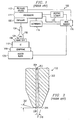
- the bonder includes a capillary tube 102 which holds a bond wire 104.
- the bond wire is typically gold.
- the end of the wire is melted to form a ball 106, typically by exposing the end of the wire to a spark.
- the ball is then pressed against a bond pad or bond site 108 of a semiconductor device or IC 110 by a pressure source 112.
- the ultrasonic transducer 114 which is driven by the ultrasonic source 116.
- the wire ball 106 is pressed against the bond pad 108, the IC 110, mounted on package or leadframe 119, and the bonder 100 are heated by heater block 120.
- the remaining portion of the bonder is represented by block 126.
- the IC 110 is any type of semiconductor device on which a bond pad 108 has been fabricated. Although any type of IC 110 is suitable, the disclosed process is optimized for bonding ICs 110 that are unable to withstand the typical bonding temperatures of 180°C, such as the DMD or other micromechanical devices. Typical ICs 110 all have a monocrystalline substrate with various metalization layers deposited thereon.
- the bond pad 108, or bonding site, is typically a small metal region on the perimeter of the IC 110 which is in electrical contact with the circuit fabricated on the IC 110.
- the bond pad 108 is made substantially of an aluminum alloy, in particular an aluminum alloy containing about 2% copper, but virtually any other metal will work.
- the wire 104 is typically 99.99% gold.
- Gold wires are preferred because in the alternative room temperature process, aluminum wire ultrasonic wedge bonding tends to produce more particle contamination during the wire bonding process. Tests have shown a 10x decrease in particle contamination using gold ball bonding at room temperature compared to aluminum wedge bonding at room temperature. Additionally, softer gold wires form stronger bonds due to increased intermetallic formation. However, harder gold wire provides better control of the wire loop profile. Therefore the optimum gold wire type is a compromise between the soft and hard types. The actual wire selected may be a function of the particular package and integrated circuit being used since those factors determine the length of the wire loops required. Typically, the softest gold wire that allows adequate control of the wire loop profile will be used.
- FIG. 2 shows a cross-sectional view of a wire bonding capillary 102 without a wire 104.
- the capillary body 202 typically a beryllium oxide or a ceramic material, encloses an inner conduit or bore 204 along a longitudinal axis 203 through which the bonding wire 104 (not shown in Figure 2 ) passes.
- the capillary body 202 tapers to a face 206 at angle called the cone angle 210.
- the capillary shown in Figure 2 has a straight taper, or cone, but capillaries are available that have a complex taper called a bottleneck. Although a cone capillary is preferred, a bottleneck capillary may also be used.
- the face 206 of the capillary is typically angled with respect to a plane normal to axis 203.
- the optimum face angle 207 for the room temperature bonding process is between 4 and 11 degrees. More particularly, a face angle 207 of 8 degrees is desired.
- the capillary includes a chamfer 208 at the intersection between the face 206 and the bore 204.
- the intersection of the chamfer 208 and face 206 surfaces reduces wire drag when the wire 104 is played out between the bonding pad 108 on the IC 110 and a similar bonding pad on a lead frame or ceramic package.
- the edge formed by the intersection of the chamfer 208 and the face 206 serves to cut or break the wire 104 after a stitch or wedge bond is formed on the lead frame.
- the grain size of the ceramic capillaries also effected the bonding process. Tests showed that the bond strength increases as the grain size of a ceramic capillary is decreased.
- the optimum capillary has a 15° cone angle although capillaries with cone angles between 20° and 10° work well.
- the preferred capillary is manufactured by Small Precision Tools Inc., although other capillaries may also be used.
- FIG. 3 shows a schematic diagram of the Abacus III bonder 304 after modification.
- a ceramic capillary 302 having a cone angle between 10 and 20 degrees, a tip diameter between 5 and 8 mils, preferably between 6.0 and 6.5 mils, a hole diameter less than 2 mils, face angle between 4 and 8 degrees, a chamfer diameter of 2.5 to 3.0 mils, and a chamfer angle between 70 and 90 degrees is used.
- An ultrasonic source 306 capable of vibrating the capillary at a frequency above 200 kHz, more particularly in the range of 235 to 245 kHz, and ideally 237 kHz, is used.
- FIG. 4 is a flow chart showing the steps involved.
- the bonding sites on the IC and the package or lead frame are subjected to a plasma cleaning process.
- a ball is formed on the end of the bond wire using an electric spark.
- the ball is then pressed against the bonding pad in block 404 with a static force of 30 to 40 grams.
- the pressure is decreased 30%.
- the ultrasonic source is then turned on in block 406 using a power between 1.0 and 1.3 watts. Compared to the 290° C prior art bond process, the ultrasonic power is increased 75%.
- a wire loop is formed 408 between the ball bond site and the site on which to form a stitch bond.
- the wire trailing out of the capillary is once again pressed against the bonding site, this time on the lead frame or package in block 410.
- the bond pressure is increased 33% above the pressure required for a 290° C stitch bond of the prior art to 40 to 50 grams.
- the ultrasonic source is turned “ON" using a power level of 1.2 to 1.4 watts, which is 70% above the level used for a 290° C stitch bond of the prior art as shown in block 412.
- the stitch bond step 412 takes 30ms, which is 50% longer than for stitch bonds of the prior art.
- the ultrasonic source is then turned “OFF" and the capillary, which has now cut the bonding wire, is withdrawn 414 leaving the completed stitch bond.
- a stitch bond may be used on either or both end of the interconnection.
Landscapes
- Engineering & Computer Science (AREA)
- Mechanical Engineering (AREA)
- Wire Bonding (AREA)
Description
- This invention relates to the field of integrated circuit (IC) interconnections. More particularly, it relates to IC interconnections utilizing high frequency ultrasonic energy, especially room-temperature IC interconnections utilizing high frequency ultrasonic energy.
- The standard technique for making circuit interconnections for semiconductor devices consists of bonding a wire, typically a gold or aluminum alloy wire, to an aluminum alloy bond pad on the semiconductor die. In the case of a gold wire, bond eventually results in an intermetallic structure of several possible phases, depending on time and temperature and dictated by diffusion behavior. The highest bond strength is obtained by maximizing the intermetallic coverage under the ball bond.
- Clean surfaces, high temperatures, and the proper amount of pressure and mechanical scrubbing contribute to an optimum reaction between the gold and aluminum metals in the wire and bond pad. Ideally, a very short bonding time may be used to create the intermetallic bond between the surfaces. While satisfactory processes have been developed for many of the typical semiconductor devices, all of the processes, known as thermosonic bond processes, rely on elevating the temperature of the semiconductor device during the bonding process.
EP 0 935 433 discloses a method of ultrasonic bonding, whereby optimum bonding is achieved at 300°C. - Unfortunately, micromechanical devices such as the Digital Micromirror Device (DMD) cannot tolerate the elevating temperature required by IC wire bonding processes of the prior art. Therefore, a room temperature wire bonding process is needed that will allow temperature sensitive devices such as the DMD to be fabricated without damaging the temperature sensitive structures.
- The problems outlined above are in large measure solved by the method and apparatus in accordance with the present invention. That is to say the invention thereof provides a wire bonding process resulting in a sufficiently strong bond being formed at ambient temperatures. The invention provides these benefits utilizing high frequency ultrasonic energy with an optimized capillary.
- According to one embodiment, the apparatus disclosed provides an ultrasonic source for vibrating a capillary tube at a frequency greater than 200 kHz, preferably at 235-245 kHz, and more preferably at 237 kHz, while a wire held in the capillary tube is pressed against a bonding site.
- Generally, the invention provides a method of forming a wire bond, the method comprising the steps of pressing a wire interconnect against a semiconductor device pad with a capillary tube and vibrating the capillary tube at a frequency above 200 kHz and using a power of 1·0 to 1·3 watts to form an intermetallic bond between the wire interconnect and the semiconductor device pad.
- For a more complete understanding of the present invention, and the advantages thereof, reference is now made to the following descriptions taken in conjunction with the accompanying drawings, in which:
-
FIGURE 1 is a schematic representation of a bonding apparatus used for bonding wire to a microelectronic integrated circuit according to the prior art; -
FIGURE 2 is a sectional view of a prior art capillary tube used for bonding wire; -
FIGURE 3 is a schematic representation of a modified bonding apparatus used for bonding wire to a microelectronic integrated circuit pad at room temperature according to the present invention; and -
FIGURE 4 is a flow chart showing the steps required to fabricate a room temperature bond using the modified bonding apparatus ofFigure 3 . - The thermosonic bond process is a widely used method of obtaining a good bond between a wire interconnect, such as a gold wire, and bond pad of a semiconductor device. Generally, this process uses low frequencies of 60 kHz to 100 kHz and temperatures of around 175° to 300°C. The present invention discloses a method of obtaining a sufficient bond between the wire interconnect and a semiconductor bond pad using increased bonding frequencies (greater than 200 kHz) and decreased temperatures (less than 100°C). The apparatus disclosed has been optimized to maximize the intermetallic bonds formed while minimizing the bonding temperature. Using this process and apparatus, strong bonds are formed at room or ambient temperatures (10° to 50°C). Furthermore, the low temperature bonding process taught herein minimizes the number of particles added during the bonding process. This is especially important when processing micromechanical devices that have moving parts, such as the DMD.
- Referring now to the drawings in general and
Figure 1 in particular, a schematic diagram of atypical wire bonder 100 of the prior art is shown. The bonder includes acapillary tube 102 which holds abond wire 104. The bond wire is typically gold. To form a ball bond, the end of the wire is melted to form aball 106, typically by exposing the end of the wire to a spark. The ball is then pressed against a bond pad orbond site 108 of a semiconductor device orIC 110 by apressure source 112. While theball 106 is pressed against thebond pad 108, the capillary 102, and thewire 104 andwire ball 106 held by the capillary 102, are vibrated at a low frequency by theultrasonic transducer 114 which is driven by theultrasonic source 116. At the same time thewire ball 106 is pressed against thebond pad 108, the IC 110, mounted on package orleadframe 119, and thebonder 100 are heated byheater block 120. Another thermal source,heating element 122, heats capillary 102 viatransducer 114. The combination of the pressure, ultrasonic vibration, and heat cause the wire ball to bond to the bond pad at theinterface 124. The remaining portion of the bonder is represented byblock 126. - The IC 110 is any type of semiconductor device on which a
bond pad 108 has been fabricated. Although any type of IC 110 is suitable, the disclosed process is optimized for bondingICs 110 that are unable to withstand the typical bonding temperatures of 180°C, such as the DMD or other micromechanical devices.Typical ICs 110 all have a monocrystalline substrate with various metalization layers deposited thereon. Thebond pad 108, or bonding site, is typically a small metal region on the perimeter of the IC 110 which is in electrical contact with the circuit fabricated on the IC 110. Typically thebond pad 108 is made substantially of an aluminum alloy, in particular an aluminum alloy containing about 2% copper, but virtually any other metal will work. - The
wire 104 is typically 99.99% gold. Gold wires are preferred because in the alternative room temperature process, aluminum wire ultrasonic wedge bonding tends to produce more particle contamination during the wire bonding process. Tests have shown a 10x decrease in particle contamination using gold ball bonding at room temperature compared to aluminum wedge bonding at room temperature. Additionally, softer gold wires form stronger bonds due to increased intermetallic formation. However, harder gold wire provides better control of the wire loop profile. Therefore the optimum gold wire type is a compromise between the soft and hard types. The actual wire selected may be a function of the particular package and integrated circuit being used since those factors determine the length of the wire loops required. Typically, the softest gold wire that allows adequate control of the wire loop profile will be used. -
Figure 2 shows a cross-sectional view of awire bonding capillary 102 without awire 104. Thecapillary body 202, typically a beryllium oxide or a ceramic material, encloses an inner conduit or bore 204 along alongitudinal axis 203 through which the bonding wire 104 (not shown inFigure 2 ) passes. Thecapillary body 202 tapers to aface 206 at angle called thecone angle 210. The capillary shown inFigure 2 has a straight taper, or cone, but capillaries are available that have a complex taper called a bottleneck. Although a cone capillary is preferred, a bottleneck capillary may also be used. Theface 206 of the capillary is typically angled with respect to a plane normal toaxis 203. Experimentation has shown that theoptimum face angle 207 for the room temperature bonding process is between 4 and 11 degrees. More particularly, aface angle 207 of 8 degrees is desired. - The capillary includes a
chamfer 208 at the intersection between theface 206 and thebore 204. The intersection of thechamfer 208 and face 206 surfaces reduces wire drag when thewire 104 is played out between thebonding pad 108 on theIC 110 and a similar bonding pad on a lead frame or ceramic package. Furthermore, the edge formed by the intersection of thechamfer 208 and theface 206 serves to cut or break thewire 104 after a stitch or wedge bond is formed on the lead frame. - Testing showed a strong interaction between the chamfer angle and the tail portion of the stitch bond. Because of the higher ultrasonic frequencies required for room temperature bonding, the amplitude of the capillary vibration is much greater than the vibration associated with bonding at elevated temperatures. The increased amplitude of vibration can prematurely cut the wire before a strong stitch bond is completed. Testing showed that a single larger chamfer angle is less likely to prematurely cut the tail of the stitch bond. Table I lists five types of capillaries tested and a summary of bond characteristics resulting from the use of each type.
Table I. Dimensions Type 1 Type 2 Type 3 Type 4 Type 5 Taper angle (deg.) 20/cone 20/btnk 20/cone 30/cone 20/btnk Tip Diameter (mils) 9.0 6.0 9.4 8.0 8.0 Outer radius (mils) 1.5 1.5 1.8 1.5 1.5 Hole diameter (mils) -- -- -- 1.5 1.5 Face angle (deg.) 8.0 4.0 8.0 8.0 11.0 finish type polished polished polished matte matte Chamfer-1 dia. (mils) 3.5 2.5 3.3 2.6 3.0 angle (deg.) 120 90 150 150 120 finish type polished polished polished matte matte Chamfer-2 dia. (mils) n/a n/a 2.8 2.0 2.8 angle (deg.) 60 finish type n/a n/a polished polished polished Findings/observations (0 = unacceptable, 1 = acceptable) Ball diameter 0 1 0 1 1 Stitch area 1 0 1 1 1 Cut stitch 1 0 0 0 0 - The tests summarized in Table I were performed using a 116 kHz ultrasonic source and a bonding temperature of 60° C. In order to reduce the bonding temperature to ambient temperatures, further studies were performed to determine the effect of capillary material, capillary geometry, lead plating metalization, and package cleaning procedures on the bond strength. The most important factor is the effect of increasing the ultrasonic frequency beyond 200 kHz. Furthermore, since frequency is inversely proportional to the amplitude of mechanical vibrations at the capillary tip, the higher frequency bonding offers additional margin against premature cutting during stitch bonding, even with a lower capillary chamfer angle. Additionally, a small capillary tip appears to magnify the effective amplitude of the ultrasonic vibration at the capillary tip.
- The grain size of the ceramic capillaries also effected the bonding process. Tests showed that the bond strength increases as the grain size of a ceramic capillary is decreased. The optimum capillary has a 15° cone angle although capillaries with cone angles between 20° and 10° work well. The preferred capillary is manufactured by Small Precision Tools Inc., although other capillaries may also be used.
- Existing wire bonders, such as the Abacus III bonder manufactured by Texas Instruments Incorporated of Dallas, Texas or the K/S 1484 bonder manufactured by Kulicke & Soffa Industries, Inc., may easily be modified to allow the implementation of the bonding process taught herein.
Figure 3 shows a schematic diagram of theAbacus III bonder 304 after modification. For optimum performance, aceramic capillary 302 having a cone angle between 10 and 20 degrees, a tip diameter between 5 and 8 mils, preferably between 6.0 and 6.5 mils, a hole diameter less than 2 mils, face angle between 4 and 8 degrees, a chamfer diameter of 2.5 to 3.0 mils, and a chamfer angle between 70 and 90 degrees is used. Anultrasonic source 306 capable of vibrating the capillary at a frequency above 200 kHz, more particularly in the range of 235 to 245 kHz, and ideally 237 kHz, is used. - The process of forming wire bonds using the modified
bonder 304 parallels the process of the prior art, but uses a higher ultrasonic frequency, bond force or pressure, ultrasonic power, and a longer bond time.Figure 4 is a flow chart showing the steps involved. Inblock 400 the bonding sites on the IC and the package or lead frame are subjected to a plasma cleaning process. In block 402 a ball is formed on the end of the bond wire using an electric spark. The ball is then pressed against the bonding pad inblock 404 with a static force of 30 to 40 grams. Compared to the prior art bond process using a 290° C bonding temperature, the pressure is decreased 30%. The ultrasonic source is then turned on inblock 406 using a power between 1.0 and 1.3 watts. Compared to the 290° C prior art bond process, the ultrasonic power is increased 75%. - After a sufficient bond time, usually 6 to 10 mSec, which is 40% longer than the 290° C prior art bond time, the ultrasonic source is shut "OFF", and the ball bond is complete.
- After forming the ball bond, a wire loop is formed 408 between the ball bond site and the site on which to form a stitch bond. The wire trailing out of the capillary is once again pressed against the bonding site, this time on the lead frame or package in
block 410. For a stitch bond, the bond pressure is increased 33% above the pressure required for a 290° C stitch bond of the prior art to 40 to 50 grams. As the wire is pressed against the bonding site, the ultrasonic source is turned "ON" using a power level of 1.2 to 1.4 watts, which is 70% above the level used for a 290° C stitch bond of the prior art as shown inblock 412. Thestitch bond step 412 takes 30ms, which is 50% longer than for stitch bonds of the prior art. The ultrasonic source is then turned "OFF" and the capillary, which has now cut the bonding wire, is withdrawn 414 leaving the completed stitch bond. Although a ball bond on the IC bonding site, and a stitch bond on the package bonding site is preferable, a stitch bond may be used on either or both end of the interconnection. - Thus, although there has been disclosed to this point a particular embodiment for a method of wire bonding at room temperature and an apparatus therefor, it is not intended that such specific references be considered as limitations upon the scope of this invention. Furthermore, having described the invention in connection with certain specific embodiments thereof, it is to be understood that further modifications may now suggest themselves to those skilled in the art.
Claims (20)
- A method of bonding a wire interconnect (106) to two sites relative to a semiconductor device (110), said method comprising:pressing (404) said wire interconnect against said semiconductor device with a capillary tube (102) having a passage (204) and tapering to a face (206), the capillary further comprising a single chamfer at an intersection between the face (206) and the passage (204) having an angle between 70 and 90 degrees; andvibrating (406) said capillary tube at a frequency above 200 kHz to form an intermetallic bond between said wire interconnect and said semiconductor device.
- The method of Claim 1, further comprising performing said step of vibrating said capillary tube using a capillary tube having a cone angle (210) of less than 20 degrees, the cone angle defined between an axis (203) through a bore (204) of the capillary tube and a taper along a body (202) and toward a face (206) of the capillary tube.
- The method of Claim 1 or Claim 2, further comprising performing said step of vibrating said capillary tube using a capillary tube having a cone angle (210) between 10 and 20 degrees, the cone angle (210) defined between an axis (203) through a bore (204) of the capillary tube and a taper along a body (202) and toward a face (206) of the capillary tube.
- The method of any preceding claim, further comprising performing said step of vibrating said capillary tube using a capillary tube having a cone angle (210) of 15 degrees, the cone angle (210) defined between an axis (203) through a bore (204) of the capillary tube and a taper along a body (202) and toward a face (206) of the capillary tube.
- The method of any preceding claim, further comprising performing said step of vibrating said capillary tube at a frequency in the range of 235 to 245 kHz.
- The method of any preceding claim, further comprising performing said step of vibrating said capillary tube at a frequency of 237 kHz.
- The method of any preceding claim, further comprising performing said step of vibrating said capillary tube for a period of 6 to 10 msec.
- The method of any preceding claim, further comprising performing said step of pressing said wire interconnect against said semiconductor device with a static force of 30 to 40 gram force.
- The method of any preceding claim, further comprising performing said wire vibrating step using a power of 1.0 to 1.3 watts.
- The method of any preceding claim, further comprising the steps of:pressing said wire interconnect against a package lead with said capillary tube; andvibrating said capillary tube at a frequency above 200kHz to form an intermetallic bond between said wire interconnect and said package lead.
- The method of Claim 10, further comprising performing the step of pressing said wire interconnect against the package lead with a static force of 40 to 50 gram force.
- The method of Claim 10 or Claim 11, further comprising performing said step of vibrating said capillary tube to form an intermetallic bond between said wire interconnect and said package lead at a frequency of 237 kHz.
- The method of any of Claims 10 to 12, further comprising performing said step of vibrating said capillary tube to form an intermetallic bond between said wire interconnect and said package lead at a power of 1.2 to 1.4 watts.
- An apparatus (100) for bonding a wire interconnect to two sites relative to a semiconductor device, said apparatus comprising:a capillary tube (102) tapering towards a face (206) and having a longitudinal passage (204) through which a wire interconnect may be passed, the capillary further comprising a single chamfer at an intersection between the face (206) and the passage (204) having an angle between 70 and 90 degrees;a high frequency transducer (114) for imparting vibrations above 200 kHz to said capillary tube; anda pressure source (112) for pressing said capillary tube towards said semiconductor device.
- The apparatus of Claim 14, wherein said capillary tube has a cone angle (210) of less than 20 degrees, the cone angle defined between an axis (203) through a bore (204) of the capillary tube and a taper along a body (202) and toward a face (206) of the capillary tube.
- The apparatus of Claim 14 or Claim 15, wherein said capillary tube has a cone angle (210) of between 20 and 10 degrees, the cone angle defined between an axis (203) through a bore (204) of the capillary tube and a taper along a body (202) and toward a face (206) of the capillary tube.
- The apparatus of any of Claims 14 to 16, wherein said capillary tube has a cone angle (210) of 15 degrees, the cone angle defined between an axis (203) through a bore (204) of the capillary tube and a taper along a body (202) and toward a face (206) of the capillary tube.
- The apparatus of any of Claims 14 to 17, wherein said transducer imparts vibrations in the range of 235 to 245 kHz to said capillary tube.
- The apparatus of any of Claims 14 to 18, wherein said transducer imparts vibrations above 240 kHz to said capillary tube.
- The apparatus of any of Claims 14 to 19, wherein said capillary tube is ceramic.
Applications Claiming Priority (2)
| Application Number | Priority Date | Filing Date | Title |
|---|---|---|---|
| US1225296P | 1996-02-26 | 1996-02-26 | |
| US12252 | 1996-02-26 |
Publications (3)
| Publication Number | Publication Date |
|---|---|
| EP0791955A2 EP0791955A2 (en) | 1997-08-27 |
| EP0791955A3 EP0791955A3 (en) | 1999-06-30 |
| EP0791955B1 true EP0791955B1 (en) | 2008-10-29 |
Family
ID=21754063
Family Applications (1)
| Application Number | Title | Priority Date | Filing Date |
|---|---|---|---|
| EP97102764A Expired - Lifetime EP0791955B1 (en) | 1996-02-26 | 1997-02-20 | Integrated circuit interconnections |
Country Status (4)
| Country | Link |
|---|---|
| US (1) | US5984162A (en) |
| EP (1) | EP0791955B1 (en) |
| JP (1) | JP3981177B2 (en) |
| DE (1) | DE69739065D1 (en) |
Families Citing this family (24)
| Publication number | Priority date | Publication date | Assignee | Title |
|---|---|---|---|---|
| US6135341A (en) * | 1998-05-27 | 2000-10-24 | Texas Instruments Incorporated | Room temperature gold wire wedge bonding process |
| US6169331B1 (en) * | 1998-08-28 | 2001-01-02 | Micron Technology, Inc. | Apparatus for electrically coupling bond pads of a microelectronic device |
| US6158647A (en) * | 1998-09-29 | 2000-12-12 | Micron Technology, Inc. | Concave face wire bond capillary |
| US20060261132A1 (en) * | 1999-02-25 | 2006-11-23 | Reiber Steven F | Low range bonding tool |
| US20070131661A1 (en) * | 1999-02-25 | 2007-06-14 | Reiber Steven F | Solder ball placement system |
| US7124927B2 (en) * | 1999-02-25 | 2006-10-24 | Reiber Steven F | Flip chip bonding tool and ball placement capillary |
| US7389905B2 (en) * | 1999-02-25 | 2008-06-24 | Reiber Steven F | Flip chip bonding tool tip |
| US20080197172A1 (en) * | 1999-02-25 | 2008-08-21 | Reiber Steven F | Bonding Tool |
| US6278191B1 (en) * | 1999-05-28 | 2001-08-21 | National Semiconductor Corporation | Bond pad sealing using wire bonding |
| JP3474132B2 (en) | 1999-09-28 | 2003-12-08 | インターナショナル・ビジネス・マシーンズ・コーポレーション | Wire bonding method and apparatus |
| US20030006267A1 (en) | 2001-06-14 | 2003-01-09 | Chen Kim H. | Room temperature gold wire bonding |
| US6715658B2 (en) * | 2001-07-17 | 2004-04-06 | Kulicke & Soffa Investments, Inc. | Ultra fine pitch capillary |
| US6910612B2 (en) | 2001-07-17 | 2005-06-28 | Kulicke & Soffa Investments, Inc. | Capillary with contained inner chamfer |
| US6500760B1 (en) * | 2001-08-02 | 2002-12-31 | Sandia Corporation | Gold-based electrical interconnections for microelectronic devices |
| JP3681676B2 (en) * | 2001-11-16 | 2005-08-10 | 松下電器産業株式会社 | Bump bonding method and apparatus |
| JP3765778B2 (en) * | 2002-08-29 | 2006-04-12 | ローム株式会社 | Capillary for wire bonding and wire bonding method using the same |
| US6786383B2 (en) * | 2002-11-14 | 2004-09-07 | Kimberly-Clark Worldwide, Inc. | Ultrasonic horn assembly with fused stack components |
| US6858943B1 (en) * | 2003-03-25 | 2005-02-22 | Sandia Corporation | Release resistant electrical interconnections for MEMS devices |
| US7407080B2 (en) * | 2004-04-02 | 2008-08-05 | Chippac, Inc. | Wire bond capillary tip |
| US20070085085A1 (en) * | 2005-08-08 | 2007-04-19 | Reiber Steven F | Dissipative pick and place tools for light wire and LED displays |
| DE102005038755B4 (en) * | 2005-08-17 | 2016-03-10 | Robert Bosch Gmbh | Micromechanical component |
| CN101996993A (en) * | 2009-08-13 | 2011-03-30 | 中芯国际集成电路制造(上海)有限公司 | Device using single metalized pad |
| US8767351B1 (en) * | 2013-01-31 | 2014-07-01 | Seagate Technology Llc | Ambient temperature ball bond |
| EP3895209A4 (en) * | 2018-12-12 | 2021-12-22 | Heraeus Materials Singapore Pte. Ltd. | PROCESS FOR ELECTRICALLY CONNECTING CONTACT SURFACES OF ELECTRONIC COMPONENTS |
Family Cites Families (6)
| Publication number | Priority date | Publication date | Assignee | Title |
|---|---|---|---|---|
| US4974767A (en) * | 1988-04-25 | 1990-12-04 | Texas Instruments Incorporated | Double cone wire bonding capillary |
| US5186378A (en) * | 1991-09-30 | 1993-02-16 | Texas Instruments Incorporated | Method and apparatus for transducer heating in low temperature bonding |
| US5201453A (en) * | 1991-09-30 | 1993-04-13 | Texas Instruments Incorporated | Linear, direct-drive microelectronic bonding apparatus and method |
| US5244140A (en) * | 1991-09-30 | 1993-09-14 | Texas Instruments Incorporated | Ultrasonic bonding process beyond 125 khz |
| US5201454A (en) * | 1991-09-30 | 1993-04-13 | Texas Instruments Incorporated | Process for enhanced intermetallic growth in IC interconnections |
| US5660319A (en) * | 1995-01-17 | 1997-08-26 | Texas Instruments Incorporated | Ultrasonic bonding process |
-
1997
- 1997-02-20 DE DE69739065T patent/DE69739065D1/en not_active Expired - Lifetime
- 1997-02-20 EP EP97102764A patent/EP0791955B1/en not_active Expired - Lifetime
- 1997-02-26 US US08/806,964 patent/US5984162A/en not_active Expired - Lifetime
- 1997-02-26 JP JP04244997A patent/JP3981177B2/en not_active Expired - Fee Related
Also Published As
| Publication number | Publication date |
|---|---|
| JP3981177B2 (en) | 2007-09-26 |
| DE69739065D1 (en) | 2008-12-11 |
| EP0791955A2 (en) | 1997-08-27 |
| US5984162A (en) | 1999-11-16 |
| EP0791955A3 (en) | 1999-06-30 |
| JPH1032230A (en) | 1998-02-03 |
Similar Documents
| Publication | Publication Date | Title |
|---|---|---|
| US5984162A (en) | Room temperature ball bonding | |
| US7500590B2 (en) | Multi-part capillary | |
| JP3996216B2 (en) | Improved capillary and fine pitch ball bonding method | |
| US5201454A (en) | Process for enhanced intermetallic growth in IC interconnections | |
| EP1381489B1 (en) | Controlled attenuation capillary | |
| EP0535433A2 (en) | Ultrasonic bonding process beyond 125 kHz | |
| US20090308911A1 (en) | Wire bonding capillary tool having multiple outer steps | |
| JP2004536456A (en) | Extra fine pitch capillary | |
| CN100540200C (en) | Capillary tube including internal ramp | |
| EP1266715A1 (en) | Gold wire bonding at room temperature | |
| WO2003000454A1 (en) | Controlled attenuation capillary with planar surface | |
| EP1189722B1 (en) | Efficient energy transfer capillary | |
| US6112973A (en) | Angled transducer-dual head bonder for optimum ultrasonic power application and flexibility for tight pitch leadframe | |
| EP2167269B1 (en) | Wire bonding capillary tool having multiple outer steps | |
| US5614113A (en) | Method and apparatus for performing microelectronic bonding using a laser | |
| US6135341A (en) | Room temperature gold wire wedge bonding process | |
| US20110068469A1 (en) | Semiconductor package with pre-formed ball bonds | |
| Dawes et al. | Ultrasonic ball/wedge bonding of aluminium wires | |
| JP2000357705A (en) | How to connect electronic components | |
| JPS615536A (en) | Capillary and wire bonding device employing it | |
| JPH11354567A (en) | Gold wire wedge bonding at room temperature | |
| JPH05129356A (en) | Bonding device of coated metallic fine wire | |
| HK1061823B (en) | Controlled attenuation capillary | |
| JPH039525A (en) | Bump forming method and its forming apparatus | |
| JP2000228421A (en) | Wedge bonding tool |
Legal Events
| Date | Code | Title | Description |
|---|---|---|---|
| PUAI | Public reference made under article 153(3) epc to a published international application that has entered the european phase |
Free format text: ORIGINAL CODE: 0009012 |
|
| AK | Designated contracting states |
Kind code of ref document: A2 Designated state(s): DE FR GB IT NL |
|
| PUAL | Search report despatched |
Free format text: ORIGINAL CODE: 0009013 |
|
| AK | Designated contracting states |
Kind code of ref document: A3 Designated state(s): DE FR GB IT NL |
|
| RIC1 | Information provided on ipc code assigned before grant |
Free format text: 6H 01L 21/607 A, 6B 23K 20/00 B |
|
| 17P | Request for examination filed |
Effective date: 19991220 |
|
| RIC1 | Information provided on ipc code assigned before grant |
Ipc: H01L 21/607 20060101ALI20080220BHEP Ipc: B23K 20/00 20060101AFI20080220BHEP |
|
| RTI1 | Title (correction) |
Free format text: INTEGRATED CIRCUIT INTERCONNECTIONS |
|
| GRAP | Despatch of communication of intention to grant a patent |
Free format text: ORIGINAL CODE: EPIDOSNIGR1 |
|
| GRAS | Grant fee paid |
Free format text: ORIGINAL CODE: EPIDOSNIGR3 |
|
| GRAA | (expected) grant |
Free format text: ORIGINAL CODE: 0009210 |
|
| AK | Designated contracting states |
Kind code of ref document: B1 Designated state(s): DE FR GB IT NL |
|
| REG | Reference to a national code |
Ref country code: GB Ref legal event code: FG4D |
|
| REF | Corresponds to: |
Ref document number: 69739065 Country of ref document: DE Date of ref document: 20081211 Kind code of ref document: P |
|
| NLV1 | Nl: lapsed or annulled due to failure to fulfill the requirements of art. 29p and 29m of the patents act | ||
| PG25 | Lapsed in a contracting state [announced via postgrant information from national office to epo] |
Ref country code: NL Free format text: LAPSE BECAUSE OF FAILURE TO SUBMIT A TRANSLATION OF THE DESCRIPTION OR TO PAY THE FEE WITHIN THE PRESCRIBED TIME-LIMIT Effective date: 20081029 |
|
| PG25 | Lapsed in a contracting state [announced via postgrant information from national office to epo] |
Ref country code: IT Free format text: LAPSE BECAUSE OF FAILURE TO SUBMIT A TRANSLATION OF THE DESCRIPTION OR TO PAY THE FEE WITHIN THE PRESCRIBED TIME-LIMIT Effective date: 20081029 |
|
| PLBE | No opposition filed within time limit |
Free format text: ORIGINAL CODE: 0009261 |
|
| STAA | Information on the status of an ep patent application or granted ep patent |
Free format text: STATUS: NO OPPOSITION FILED WITHIN TIME LIMIT |
|
| 26N | No opposition filed |
Effective date: 20090730 |
|
| PGFP | Annual fee paid to national office [announced via postgrant information from national office to epo] |
Ref country code: FR Payment date: 20120203 Year of fee payment: 16 |
|
| PGFP | Annual fee paid to national office [announced via postgrant information from national office to epo] |
Ref country code: DE Payment date: 20120229 Year of fee payment: 16 |
|
| PGFP | Annual fee paid to national office [announced via postgrant information from national office to epo] |
Ref country code: GB Payment date: 20120127 Year of fee payment: 16 |
|
| GBPC | Gb: european patent ceased through non-payment of renewal fee |
Effective date: 20130220 |
|
| REG | Reference to a national code |
Ref country code: FR Ref legal event code: ST Effective date: 20131031 |
|
| REG | Reference to a national code |
Ref country code: DE Ref legal event code: R119 Ref document number: 69739065 Country of ref document: DE Effective date: 20130903 |
|
| PG25 | Lapsed in a contracting state [announced via postgrant information from national office to epo] |
Ref country code: GB Free format text: LAPSE BECAUSE OF NON-PAYMENT OF DUE FEES Effective date: 20130220 Ref country code: DE Free format text: LAPSE BECAUSE OF NON-PAYMENT OF DUE FEES Effective date: 20130903 Ref country code: FR Free format text: LAPSE BECAUSE OF NON-PAYMENT OF DUE FEES Effective date: 20130228 |