EP0776059B1 - Switchable duplex filter - Google Patents
Switchable duplex filter Download PDFInfo
- Publication number
- EP0776059B1 EP0776059B1 EP96308466A EP96308466A EP0776059B1 EP 0776059 B1 EP0776059 B1 EP 0776059B1 EP 96308466 A EP96308466 A EP 96308466A EP 96308466 A EP96308466 A EP 96308466A EP 0776059 B1 EP0776059 B1 EP 0776059B1
- Authority
- EP
- European Patent Office
- Prior art keywords
- filter
- resonators
- port
- regulating element
- radio frequency
- Prior art date
- Legal status (The legal status is an assumption and is not a legal conclusion. Google has not performed a legal analysis and makes no representation as to the accuracy of the status listed.)
- Expired - Lifetime
Links
- 230000005540 biological transmission Effects 0.000 claims description 49
- 230000008878 coupling Effects 0.000 claims description 29
- 238000010168 coupling process Methods 0.000 claims description 29
- 238000005859 coupling reaction Methods 0.000 claims description 29
- 230000001105 regulatory effect Effects 0.000 claims description 23
- 239000004020 conductor Substances 0.000 claims description 10
- 230000001939 inductive effect Effects 0.000 description 8
- 239000000919 ceramic Substances 0.000 description 4
- 238000010586 diagram Methods 0.000 description 4
- 239000004065 semiconductor Substances 0.000 description 4
- 229910010293 ceramic material Inorganic materials 0.000 description 3
- 239000003990 capacitor Substances 0.000 description 2
- 239000011248 coating agent Substances 0.000 description 2
- 238000000576 coating method Methods 0.000 description 2
- 230000002301 combined effect Effects 0.000 description 2
- 238000004891 communication Methods 0.000 description 2
- 238000010276 construction Methods 0.000 description 2
- 230000005669 field effect Effects 0.000 description 2
- JBRZTFJDHDCESZ-UHFFFAOYSA-N AsGa Chemical compound [As]#[Ga] JBRZTFJDHDCESZ-UHFFFAOYSA-N 0.000 description 1
- 239000000654 additive Substances 0.000 description 1
- 230000000996 additive effect Effects 0.000 description 1
- 230000001276 controlling effect Effects 0.000 description 1
- 230000003247 decreasing effect Effects 0.000 description 1
- 239000012799 electrically-conductive coating Substances 0.000 description 1
- 230000005672 electromagnetic field Effects 0.000 description 1
- 238000005516 engineering process Methods 0.000 description 1
- 238000007667 floating Methods 0.000 description 1
- 239000011810 insulating material Substances 0.000 description 1
- 238000004519 manufacturing process Methods 0.000 description 1
- 238000005259 measurement Methods 0.000 description 1
- 229910052751 metal Inorganic materials 0.000 description 1
- 239000002184 metal Substances 0.000 description 1
- 238000000034 method Methods 0.000 description 1
- 238000010295 mobile communication Methods 0.000 description 1
- 238000005476 soldering Methods 0.000 description 1
- 239000000758 substrate Substances 0.000 description 1
- 230000003313 weakening effect Effects 0.000 description 1
Images


Classifications
-
- H—ELECTRICITY
- H01—ELECTRIC ELEMENTS
- H01P—WAVEGUIDES; RESONATORS, LINES, OR OTHER DEVICES OF THE WAVEGUIDE TYPE
- H01P1/00—Auxiliary devices
- H01P1/20—Frequency-selective devices, e.g. filters
- H01P1/213—Frequency-selective devices, e.g. filters combining or separating two or more different frequencies
- H01P1/2136—Frequency-selective devices, e.g. filters combining or separating two or more different frequencies using comb or interdigital filters; using cascaded coaxial cavities
Definitions
- the invention relates to frequency response control in a filter which is based on transmission line resonators.
- controlling is focused especially on the location of the pass band of a bandpass filter on the frequency axis.
- the invention can be applied in duplex filters, in particular.
- Filters based on transmission line resonators and electromagnetic couplings between them are generally used in radio equipment. Between the transmission line resonators, which are coupled through an insulating material by means of electromagnetic fields, there generally occurs both a capacitive and an inductive coupling, which together result in a certain frequency response in the filter constituted by the resonators. Particularly said capacitive and inductive couplings together may cause in the frequency response of the bandpass filter a transmission zero, or a certain narrow frequency range, which limits the pass band of the filter on one side and in which the attenuation of the filter is particularly high.
- ⁇ /4 resonators i.e.
- the location of said transmission zero with respect to the pass band of the filter depends on the mutual intensities of the capacitive and inductive couplings between the resonators. If the capacitive coupling is dominant, the transmission zero is located below the pass band, and if the inductive coupling is dominant, the transmission zero is located above the pass band.
- duplex filter which as a generic term refers to a filter that separates the transmitted signal and received signal from each other in radio equipment where transmission and reception take place via the same antenna at different frequencies.
- the prior art duplex filter is a three-port circuit device, which comprises a transmitter port, a receiver port and an antenna port. A radio signal brought to the transmitter port at a certain transmission frequency sees the signal path leading to the receiver port as a high impedance, in which case the radio power of transmission frequency is not directed in any substantial amount to the receiver port, but it is directed through the antenna port to the antenna, from which it is radiated as a radio signal to the environment.
- the radio signal of the reception frequency which comes via the antenna and antenna port sees the direction of the transmitter port as a high impedance, whereby it is directed to the receiver port and through it to the receiver parts of the radio equipment.
- the difference between the transmission and reception frequencies is called a duplex interval.
- the size of filters is a very critical factor.
- duplex filter which comprises transmission line resonators
- a certain number of resonators are needed in the transmission branch (between the transmitter port and the antenna port) and similarly, a certain number of resonators are needed in the receiving branch (between the antenna port and the receiver port).
- the number of resonators depends, among other factors, on the stop attenuation required, that is, how precisely the transmission frequency signal must be prevented from entering the receiving branch.
- a problem to be encountered is how the size of the filter can be decreased without making compromises in the performance.
- Figure 1 shows a prior art ceramic duplex filter, the frame block 1 of which is manufactured from dielectric ceramic material. In it there have been formed four resonator holes 2, the inner surfaces of which are coated with electrically conductive material, preferably a metal coating. On the visible side of the frame block there are formed switching patterns of electrically conductive material, which patterns comprise a transmitter port TX, an antenna port ANT and a receiving port RX. In the Figure, the darkened surface areas of block 1 depict uncoated portions and the white areas correspond to the electrically conductive coating.
- a strip conductor pattern 3 which influences - in a manner known from previously mentioned patent specifications - on the electromagnetic coupling between the resonators and thereby on the frequency response of the transmission filter formed by the resonators.
- a dielectric bandpass filter in which the pass band can be shifted by switches.
- the filter has one discrete capacitor and one switch for each resonator. For changing the response of the filter the one pole of each capacitor is connected to ground by a switch.
- the filter also has input and output switches to form a duplexer.
- One disadvantage of the filter is that the form of the amplitude response does not change, when the pass band is shifted. It would be advantageous to arrange an attenuation peak on that side of the pass band, where the other of transmitting/receiving bands is located.
- An object of the invention is to provide a novel and more advantageous way to realize a duplex filter.
- a duplex filter according to the invention is characterized in that which is expressed in the independent claim 1.
- Advantageous embodiments of the invention are disclosed in the other claims.
- Embodiments in accordance with the invention is based on the idea that the pass band and the respective limiting transmission zero of a resonator-based radio frequency filter can be moved with the electric control signal so that a filter constituted by the same resonators can operate, depending on the control signal, either as a transmission or reception filter in radio equipment in which transmission and reception take place on different frequency bands.
- the control signal is set to influence the potential of a certain regulating element located in the vicinity of the resonators.
- the pass band of the filter covers the transmission frequency band and the transmission zero may be in the reception frequency, whereby the transmission frequency signal gets through the filter but the reception frequencies are filtered away.
- the pass band of the filter is in the reception frequency and the transmission zero is in the transmission frequency, whereby only the reception frequency signal gets through the filter. Because the same resonators may be used to implement both the transmission and reception filter, the total number of transmission line resonators needed in the radio equipment is smaller than in the prior art solutions, and the filter has very small physical dimensions.
- the filter in accordance with the invention is a duplex filter, which has only two ports.
- the first port is an antenna port, which is continuously coupled to the antenna of the radio equipment.
- the second port is switched by a separate switching means alternately to the transmitter or receiver of the radio equipment, depending on whether the filter is set by the control signal to operate as a transmission filter or a reception filter.
- the control of the switching means and the control signal that affects the properties of the filter operate in synchronization.
- the switching means corresponds to the antenna switch which is known as such, and it can be any electrically controlled switch, known to a person skilled in the art, preferably a PIN diode or a combination thereof, a field-effect transistor (FET) or other voltage and/or current controlled semiconductor switch.
- FET field-effect transistor
- the potential of the regulating element is also changed, preferably by a semiconductor switch connected to it.
- the semiconductor switches are made of gallium arsenide (GaAs), for example, they can be made fast and reliable, and thus it is possible to change the frequency response of the filter very fast between two different states.
- the regulating element by which a filter in accordance with the invention is changed from a transmission filter to a reception filter and vice versa by changing the potential thereof, is constituted by a certain electrically conductive device, which is located in the vicinity of the resonators and affects the electromagnetic coupling between them.
- the filter in accordance with the invention comprises dielectric resonators formed in a ceramic block
- the electrically conductive device is preferably a strip conductor formed on the surface of the ceramic frame block.
- the corresponding electrically conductive device is preferably formed as a strip conductor on the surface of a low loss circuit board which operates as the support structure of a helix resonator.
- the capacitive coupling between the transmission line resonators is strongest at their (electrically) open, ungrounded end.
- the inductive coupling is strongest at the grounded end of the resonators.
- the regulating element is preferably formed near the open end of the resonators, whereby it, ungrounded, strengthens the capacitive coupling.
- the grounding of the element weakens the capacitive coupling, whereby the inductive coupling becomes dominant in the combined effect of the couplings.
- An electrically controllable switch connected between the regulating element and the ground potential is used for the grounding.
- the filter 4 in accordance with the invention comprises an antenna port ANT and a radio equipment port TX/RX.
- it comprises a control signal input CONTROL, whereby it depends on the control signal brought to it whether the filter 4 operates as a transmission or reception filter.
- the duplex filter arrangement according to the invention also includes a switch 5, which switches the radio equipment port TX/RX of the filter to the transmitter or receiver of the radio equipment in synchronization with the control signal CONTROL.
- Figure 3 shows a circuit diagram, in which there is between two transmission line resonators 6, 7 an electrically conductive regulating element 8, which influences the coupling between the resonators 6 and 7.
- the regulating element 8 can be grounded with switch 9, if desired.
- switch 9 When switch 9 is closed, the regulating element 8 in the vicinity of the open end of resonators 6 and 7 is essentially at ground potential, whereby it weakens the capacitive coupling between the resonators.
- the electromagnetic coupling between the resonators is dominantly inductive, and so the frequency response formed by the resonators has the transmission zero above the pass band. If the transmission frequency of the radio equipment is lower than its receiving frequency, the filter is a transmission filter.
- the regulating element 8 When switch 9 is opened, the regulating element 8 has a floating potential, whereby it strengthens the capacitive coupling between the resonators 6 and 7, and as a combined effect, the coupling of the resonators is dominantly capacitive.
- the transmission zero of the frequency response moves below the pass band, and the pass band moves upwards by a duplex interval, whereby the same filter operates as a reception filter.
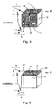
- Figure 4 shows a dielectric filter made of one piece (a so-called monoblock), which includes two transmission line resonators 6 and 7.
- the manufacture of filters like this is a technique known to a person skilled in the art, and it will not be dealt with here.
- the dielectric block 10, which constitutes the body of the filter is preferably of ceramic material, and the resonators 6 and 7 are cylindrical holes in the block, extending from the lower surface of block 10 to its upper surface (the top surface in the figure) of the block.
- the cylindrical surfaces that define the holes have a conductive coating.
- the resonator holes can also be physically closed at the ungrounded end.
- Most of the side surfaces of the block 10 are also coated with a conductive material, which is shown by white colour in the figure.
- the front side shown in Figure 4 is not entirely coated, but strip-like conductive patterns 11, 12 and 13 have been formed on it.
- the top side shown in Figure 4 is uncoated.
- the uncoated ceramic material is shown as grey in the Figure.
- the two widest conductive patterns 11 and 12 constitute the input and output ports of the filter, i.e. they provide the coupling interface to the resonators 6 and 7.
- the third conductor pattern 13 is a regulating element, which strengthens the capacitive coupling between the resonators 6 and 7 in a known manner, when ungrounded.
- the alternative embodiment shown in Figure 5 is also a dielectric filter, which differs from the embodiment of Figure 4 only in that here also the front side is coated with a conductive layer, and the conductive patterns 11, 12 and 13 are formed on the top surface, which is uncoated except for said conductive patterns.
- the embodiments shown in Figures 3, 4 and 5 comprise a switch 9, which is shown in the figures as a general outline.
- a person skilled in the art is readily capable of realizing such a switch with a PIN diode, a field-effect transistor or other semiconductor switch known as such.
- the switch component in question is connected by soldering, for example, to connection pads (not shown in the figures), which are formed on the surface of the dielectric block 10 in the same manner as the other conductive patterns 11, 12 and 13.
- the control signal CONTROL which opens and closes the switch 9, is coupled to said switch component using strip lines (not shown in the figures) formed on the surface of the dielectric block.
- the switch 9 is open in the position shown in the figures 3, 4 and 5, whereby it does not substantially influence the operation of the filter.
- the switch 9 When the switch 9 is closed, it couples the regulating element 13 to ground potential, whereby the grounded regulating element 13 weakens the capacitive coupling between the resonators 6 and 7.
- the weakening of the capacitive coupling strengthens the relative portion of the inductive coupling, which in turn moves the transmission zero of the frequency response of the filter upwards on the frequency axis.
- Figure 6 shows a qualitative presentation of a real frequency response measurement, in which the frequency response of a filter according to the embodiment shown in Figure 3 is measured while the switch 9 is closed (curve 14) and open (curve 15).
- Figure 6 shows that closing the switch 9 (grounding the regulating element 13) turns the frequency response almost into a mirror image in relation to an assumed axis, which is located half-way between the transmission band TX' and the reception band RX'.
- the filter causes only a weak attenuation on the transmission band TX', but a strong attenuation on the frequencies of the reception band RX'.
- the pass band and the stop band have changed places.
- the switch shown schematically in figures 3, 4 and 5, the purpose of which is to switch the radio equipment port 11 of the filter alternately to the transmitter and receiver of the radio equipment, corresponds in its component arrangement to the switch 9, and it can be connected to connection pads on the surface of the dielectric block 10, or it can be situated on the surface of a substrate plate which is part of the filter, or on the surface of a circuit board (not shown in the figures) of the radio equipment.
- a control signal is brought to it, which signal is the same or in the same phase as the signal brought to switch 9.
- the switch 5 With the first value of the control signal CONTROL, the switch 5 switches the radio equipment port 11 of the filter to the transmitter (not shown in the figure) of the radio equipment, whereby the switch 9 is also closed and the pass band of the filter is located in the transmission frequency.
- the switch 5 switches the radio equipment port 11 of the filter to the receiver (not shown in the figure) of the radio equipment. Then the switch 9 is open and the filter passes the reception frequency and filters the transmission and other undesired frequencies.
- the frequency response of a two-port filter which preferably comprises only two resonators can be set alternately to correspond to the transmission and reception branch of an ordinary duplex filter.
- the change of the frequency response takes place fast and easily.
- a very small duplex filter can be achieved by providing the filter with a change-over switch.
- the invention is not limited to dielectric filters only, but it can be applied to all filter constructions which are based on transmission line resonators and in which the coupling between the resonators can be influenced by a conductive regulating element.
- Another possible exemplary filter construction is a helix filter based on cylindrical coil conductors, the like of which is known, for example, from the Finnish patent specification Fl-90157, wherein the regulating elements according to the invention can be manufactured as strip lines in a similar manner as in the embodiments described above. Filters according to the invention can be advantageously used in small radio communication devices, such as mobile phones.
Landscapes
- Control Of Motors That Do Not Use Commutators (AREA)
- Transceivers (AREA)
Description
- The invention relates to frequency response control in a filter which is based on transmission line resonators. In a filter in accordance with the invention, controlling is focused especially on the location of the pass band of a bandpass filter on the frequency axis. The invention can be applied in duplex filters, in particular.
- Filters based on transmission line resonators and electromagnetic couplings between them are generally used in radio equipment. Between the transmission line resonators, which are coupled through an insulating material by means of electromagnetic fields, there generally occurs both a capacitive and an inductive coupling, which together result in a certain frequency response in the filter constituted by the resonators. Particularly said capacitive and inductive couplings together may cause in the frequency response of the bandpass filter a transmission zero, or a certain narrow frequency range, which limits the pass band of the filter on one side and in which the attenuation of the filter is particularly high. In a filter which is based on so-called λ/4 resonators, i.e. in which the electric length of the resonators is essentially one fourth of the wavelength corresponding to the nominal frequency of the filter, the location of said transmission zero with respect to the pass band of the filter depends on the mutual intensities of the capacitive and inductive couplings between the resonators. If the capacitive coupling is dominant, the transmission zero is located below the pass band, and if the inductive coupling is dominant, the transmission zero is located above the pass band.
- Using bandpass filters it is possible to implement a duplex filter, which as a generic term refers to a filter that separates the transmitted signal and received signal from each other in radio equipment where transmission and reception take place via the same antenna at different frequencies. The prior art duplex filter is a three-port circuit device, which comprises a transmitter port, a receiver port and an antenna port. A radio signal brought to the transmitter port at a certain transmission frequency sees the signal path leading to the receiver port as a high impedance, in which case the radio power of transmission frequency is not directed in any substantial amount to the receiver port, but it is directed through the antenna port to the antenna, from which it is radiated as a radio signal to the environment. Similarly, the radio signal of the reception frequency which comes via the antenna and antenna port sees the direction of the transmitter port as a high impedance, whereby it is directed to the receiver port and through it to the receiver parts of the radio equipment. The difference between the transmission and reception frequencies is called a duplex interval.
- In modern radio communication devices, such as mobile phones, the size of filters is a very critical factor. In a prior art duplex filter, which comprises transmission line resonators, a certain number of resonators are needed in the transmission branch (between the transmitter port and the antenna port) and similarly, a certain number of resonators are needed in the receiving branch (between the antenna port and the receiver port). The number of resonators depends, among other factors, on the stop attenuation required, that is, how precisely the transmission frequency signal must be prevented from entering the receiving branch. When the size of mobile communication devices is further reduced, a problem to be encountered is how the size of the filter can be decreased without making compromises in the performance.
- Figure 1 shows a prior art ceramic duplex filter, the
frame block 1 of which is manufactured from dielectric ceramic material. In it there have been formed fourresonator holes 2, the inner surfaces of which are coated with electrically conductive material, preferably a metal coating. On the visible side of the frame block there are formed switching patterns of electrically conductive material, which patterns comprise a transmitter port TX, an antenna port ANT and a receiving port RX. In the Figure, the darkened surface areas ofblock 1 depict uncoated portions and the white areas correspond to the electrically conductive coating. At the two rightmost resonators there is formed astrip conductor pattern 3, which influences - in a manner known from previously mentioned patent specifications - on the electromagnetic coupling between the resonators and thereby on the frequency response of the transmission filter formed by the resonators. - From the
publication EP 0 614 244 is known a dielectric filter, which is manufactured like the filter in figure 1. The structure comprises also two additive conductive areas on the surface of frame block and four switches. By means of these a coupling between resonators can be changed so that the filter either attenuates or passes signals at certain operation band. The filter in question can not function as a duplexer. - From the
publication EP 0 654 912 is known a dielectric bandpass filter, in which the pass band can be shifted by switches. The filter has one discrete capacitor and one switch for each resonator. For changing the response of the filter the one pole of each capacitor is connected to ground by a switch. The filter also has input and output switches to form a duplexer. One disadvantage of the filter is that the form of the amplitude response does not change, when the pass band is shifted. It would be advantageous to arrange an attenuation peak on that side of the pass band, where the other of transmitting/receiving bands is located. - An object of the invention is to provide a novel and more advantageous way to realize a duplex filter. A duplex filter according to the invention is characterized in that which is expressed in the
independent claim 1. Advantageous embodiments of the invention are disclosed in the other claims. - Embodiments in accordance with the invention is based on the idea that the pass band and the respective limiting transmission zero of a resonator-based radio frequency filter can be moved with the electric control signal so that a filter constituted by the same resonators can operate, depending on the control signal, either as a transmission or reception filter in radio equipment in which transmission and reception take place on different frequency bands. The control signal is set to influence the potential of a certain regulating element located in the vicinity of the resonators. With a certain first value thereof, the pass band of the filter covers the transmission frequency band and the transmission zero may be in the reception frequency, whereby the transmission frequency signal gets through the filter but the reception frequencies are filtered away. With a certain second -value of the control signal and similarly the potential of the regulating element, the pass band of the filter is in the reception frequency and the transmission zero is in the transmission frequency, whereby only the reception frequency signal gets through the filter. Because the same resonators may be used to implement both the transmission and reception filter, the total number of transmission line resonators needed in the radio equipment is smaller than in the prior art solutions, and the filter has very small physical dimensions.
- The filter in accordance with the invention is a duplex filter, which has only two ports. The first port is an antenna port, which is continuously coupled to the antenna of the radio equipment. The second port is switched by a separate switching means alternately to the transmitter or receiver of the radio equipment, depending on whether the filter is set by the control signal to operate as a transmission filter or a reception filter. The control of the switching means and the control signal that affects the properties of the filter operate in synchronization. The switching means corresponds to the antenna switch which is known as such, and it can be any electrically controlled switch, known to a person skilled in the art, preferably a PIN diode or a combination thereof, a field-effect transistor (FET) or other voltage and/or current controlled semiconductor switch. The potential of the regulating element is also changed, preferably by a semiconductor switch connected to it. If the semiconductor switches are made of gallium arsenide (GaAs), for example, they can be made fast and reliable, and thus it is possible to change the frequency response of the filter very fast between two different states.
- The regulating element, by which a filter in accordance with the invention is changed from a transmission filter to a reception filter and vice versa by changing the potential thereof, is constituted by a certain electrically conductive device, which is located in the vicinity of the resonators and affects the electromagnetic coupling between them. If the filter in accordance with the invention comprises dielectric resonators formed in a ceramic block, the electrically conductive device is preferably a strip conductor formed on the surface of the ceramic frame block. If the filter is implemented by helix resonator technology, the corresponding electrically conductive device is preferably formed as a strip conductor on the surface of a low loss circuit board which operates as the support structure of a helix resonator.
- The capacitive coupling between the transmission line resonators is strongest at their (electrically) open, ungrounded end. The inductive coupling is strongest at the grounded end of the resonators. The regulating element is preferably formed near the open end of the resonators, whereby it, ungrounded, strengthens the capacitive coupling. The grounding of the element weakens the capacitive coupling, whereby the inductive coupling becomes dominant in the combined effect of the couplings. An electrically controllable switch connected between the regulating element and the ground potential is used for the grounding.
- In the following, embodiments of the invention will be described in more detail with reference to the appended drawings, in which
- Figure 1
- shows a prior art ceramic duplex filter,
- Figure 2
- shows a diagram of a principle in accordance with the invention,
- Figure 3
- shows a circuit diagram of one embodiment for implementing the invention,
- Figure 4
- shows one preferred embodiment of the invention,
- Figure 5
- shows another preferred embodiment of the invention, and
- Figure 6
- is a qualitative diagram of the frequency response properties that can be achieved by the embodiments of the invention according to Figures 4 and 5.
- In accordance with the principle shown in Figure 2, the
filter 4 in accordance with the invention comprises an antenna port ANT and a radio equipment port TX/RX. In addition, it comprises a control signal input CONTROL, whereby it depends on the control signal brought to it whether thefilter 4 operates as a transmission or reception filter. The duplex filter arrangement according to the invention also includes aswitch 5, which switches the radio equipment port TX/RX of the filter to the transmitter or receiver of the radio equipment in synchronization with the control signal CONTROL. - Figure 3 shows a circuit diagram, in which there is between two
transmission line resonators resonators switch 9, if desired. Whenswitch 9 is closed, the regulating element 8 in the vicinity of the open end ofresonators switch 9 is opened, the regulating element 8 has a floating potential, whereby it strengthens the capacitive coupling between theresonators - Figure 4 shows a dielectric filter made of one piece (a so-called monoblock), which includes two
transmission line resonators dielectric block 10, which constitutes the body of the filter, is preferably of ceramic material, and theresonators block 10 to its upper surface (the top surface in the figure) of the block. The cylindrical surfaces that define the holes have a conductive coating. The resonator holes can also be physically closed at the ungrounded end. Most of the side surfaces of theblock 10 are also coated with a conductive material, which is shown by white colour in the figure. The front side shown in Figure 4 is not entirely coated, but strip-likeconductive patterns conductive patterns resonators third conductor pattern 13 is a regulating element, which strengthens the capacitive coupling between theresonators - The alternative embodiment shown in Figure 5 is also a dielectric filter, which differs from the embodiment of Figure 4 only in that here also the front side is coated with a conductive layer, and the
conductive patterns - In accordance with the invention, the embodiments shown in Figures 3, 4 and 5 comprise a
switch 9, which is shown in the figures as a general outline. A person skilled in the art is readily capable of realizing such a switch with a PIN diode, a field-effect transistor or other semiconductor switch known as such. In the implementation, the switch component in question is connected by soldering, for example, to connection pads (not shown in the figures), which are formed on the surface of thedielectric block 10 in the same manner as the otherconductive patterns switch 9, is coupled to said switch component using strip lines (not shown in the figures) formed on the surface of the dielectric block. - The
switch 9 is open in the position shown in the figures 3, 4 and 5, whereby it does not substantially influence the operation of the filter. When theswitch 9 is closed, it couples the regulatingelement 13 to ground potential, whereby the grounded regulatingelement 13 weakens the capacitive coupling between theresonators switch 9 is closed (curve 14) and open (curve 15). Figure 6 shows that closing the switch 9 (grounding the regulating element 13) turns the frequency response almost into a mirror image in relation to an assumed axis, which is located half-way between the transmission band TX' and the reception band RX'. In a transmission situation depicted by thecurve 14, the filter causes only a weak attenuation on the transmission band TX', but a strong attenuation on the frequencies of the reception band RX'. In the situation ofcurve 15, the pass band and the stop band have changed places. - The switch shown schematically in figures 3, 4 and 5, the purpose of which is to switch the
radio equipment port 11 of the filter alternately to the transmitter and receiver of the radio equipment, corresponds in its component arrangement to theswitch 9, and it can be connected to connection pads on the surface of thedielectric block 10, or it can be situated on the surface of a substrate plate which is part of the filter, or on the surface of a circuit board (not shown in the figures) of the radio equipment. A control signal is brought to it, which signal is the same or in the same phase as the signal brought to switch 9. With the first value of the control signal CONTROL, theswitch 5 switches theradio equipment port 11 of the filter to the transmitter (not shown in the figure) of the radio equipment, whereby theswitch 9 is also closed and the pass band of the filter is located in the transmission frequency. With the second value of the control signal, theswitch 5 switches theradio equipment port 11 of the filter to the receiver (not shown in the figure) of the radio equipment. Then theswitch 9 is open and the filter passes the reception frequency and filters the transmission and other undesired frequencies. - In a filter in accordance with the invention, the frequency response of a two-port filter which preferably comprises only two resonators can be set alternately to correspond to the transmission and reception branch of an ordinary duplex filter. The change of the frequency response takes place fast and easily. A very small duplex filter can be achieved by providing the filter with a change-over switch.
- The invention is not limited to dielectric filters only, but it can be applied to all filter constructions which are based on transmission line resonators and in which the coupling between the resonators can be influenced by a conductive regulating element. Another possible exemplary filter construction is a helix filter based on cylindrical coil conductors, the like of which is known, for example, from the Finnish patent specification Fl-90157, wherein the regulating elements according to the invention can be manufactured as strip lines in a similar manner as in the embodiments described above. Filters according to the invention can be advantageously used in small radio communication devices, such as mobile phones.
Claims (6)
- A radio frequency filter, which comprisesa first transmission line resonator and a second transmission line resonator, having an electromagnetic coupling therebetween,a first port for conducting a signal between the radio frequency filter and an antenna and a second port for conducting a signal between the radio frequency filter and other parts of a radio equipment,a regulating element for affecting the electromagnetic coupling,first switching means between the regulating element and a ground for changing the potential of the regulating element andsecond switching means between the second port and the transmitting and receiving part of said radio equipment to connect the second port alternatively to the transmitting part or the receiving part, being arranged to operate in synchronization with the first switching means, characterized in thatsaid regulating element (13) consists of a single conductor and extends in length substantially between said resonators (6, 7) to move a transmission zero of frequency response of the filter,said first switching means (9) has a single switch, andsaid second switching means (5) has a single switch.
- A radio frequency filter according to claim 1, characterized in that said regulating element (13) is arranged to strengthen the electromagnetic coupling between said first (6) and second (7) transmission line resonators, when ungrounded.
- A radio frequency filter according to claim 1, characterized in that it comprises a frame block (10) and that the transmission line resonators (6, 7) are dielectric resonators formed in said frame block.
- A radio frequency filter according to claim 4, characterized in that said regulating element, first port and second port are conductive patterns on a surface of said frame block.
- A radio frequency filter according to claim 1, characterized in that said transmission line resonators are helix resonators implemented as cylindrical coil conductors.
- A radio frequency filter according to claim 5, characterized in that it comprises a circuit board, which supports said helix resonators, and said regulating element, first port and second port are conductive patterns on a surface of the circuit board.
Applications Claiming Priority (2)
| Application Number | Priority Date | Filing Date | Title |
|---|---|---|---|
| FI955637A FI99174C (en) | 1995-11-23 | 1995-11-23 | Switchable duplex filter |
| FI955637 | 1995-11-23 |
Publications (3)
| Publication Number | Publication Date |
|---|---|
| EP0776059A2 EP0776059A2 (en) | 1997-05-28 |
| EP0776059A3 EP0776059A3 (en) | 1998-03-18 |
| EP0776059B1 true EP0776059B1 (en) | 2003-01-22 |
Family
ID=8544431
Family Applications (1)
| Application Number | Title | Priority Date | Filing Date |
|---|---|---|---|
| EP96308466A Expired - Lifetime EP0776059B1 (en) | 1995-11-23 | 1996-11-22 | Switchable duplex filter |
Country Status (7)
| Country | Link |
|---|---|
| US (1) | US5815048A (en) |
| EP (1) | EP0776059B1 (en) |
| JP (1) | JPH09181502A (en) |
| AU (1) | AU720171B2 (en) |
| CA (1) | CA2185384A1 (en) |
| DE (1) | DE69625886T2 (en) |
| FI (1) | FI99174C (en) |
Families Citing this family (45)
| Publication number | Priority date | Publication date | Assignee | Title |
|---|---|---|---|---|
| US6466613B1 (en) * | 1999-04-26 | 2002-10-15 | Itran Communications Ltd. | Communications transceiver utilizing a single filter |
| JP3613156B2 (en) * | 2000-01-18 | 2005-01-26 | 株式会社村田製作所 | Dielectric filter, antenna duplexer, and communication device |
| DE60110827T2 (en) | 2000-11-03 | 2006-01-12 | Paratek Microwave, Inc. | CHANNEL FREQUENCY DISTRIBUTION METHOD FOR HF AND MICROWAVE DUPLEXERS |
| JP2003060408A (en) * | 2001-06-05 | 2003-02-28 | Murata Mfg Co Ltd | Filter parts and communication equipment |
| TWI364175B (en) * | 2003-08-28 | 2012-05-11 | Gct Semiconductor Inc | System and method for filtering signals in a transceiver |
| CN1989652B (en) | 2004-06-28 | 2013-03-13 | 脉冲芬兰有限公司 | Antenna component |
| CN101390248B (en) * | 2004-12-09 | 2012-12-05 | 维斯普瑞公司 | Pole-zero elements and related systems and methods |
| FI20055420A0 (en) | 2005-07-25 | 2005-07-25 | Lk Products Oy | Adjustable multi-band antenna |
| FI119009B (en) | 2005-10-03 | 2008-06-13 | Pulse Finland Oy | Multiple-band antenna |
| FI118782B (en) | 2005-10-14 | 2008-03-14 | Pulse Finland Oy | Adjustable antenna |
| FI119577B (en) * | 2005-11-24 | 2008-12-31 | Pulse Finland Oy | The multiband antenna component |
| JP4621155B2 (en) * | 2006-02-28 | 2011-01-26 | 株式会社エヌ・ティ・ティ・ドコモ | Variable filter |
| US8618990B2 (en) | 2011-04-13 | 2013-12-31 | Pulse Finland Oy | Wideband antenna and methods |
| DE102006046190B4 (en) | 2006-09-29 | 2016-09-01 | Intel Deutschland Gmbh | Circuit arrangement, method for operating a circuit arrangement and method for operating a dual-mode UMTS / GSM mobile telephone |
| US10211538B2 (en) | 2006-12-28 | 2019-02-19 | Pulse Finland Oy | Directional antenna apparatus and methods |
| FI20075269A0 (en) | 2007-04-19 | 2007-04-19 | Pulse Finland Oy | Method and arrangement for antenna matching |
| FI120427B (en) | 2007-08-30 | 2009-10-15 | Pulse Finland Oy | Adjustable multiband antenna |
| FI20096134A0 (en) | 2009-11-03 | 2009-11-03 | Pulse Finland Oy | Adjustable antenna |
| FI20096251A0 (en) | 2009-11-27 | 2009-11-27 | Pulse Finland Oy | MIMO antenna |
| US8847833B2 (en) | 2009-12-29 | 2014-09-30 | Pulse Finland Oy | Loop resonator apparatus and methods for enhanced field control |
| FI20105158L (en) | 2010-02-18 | 2011-08-19 | Pulse Finland Oy | ANTENNA EQUIPPED WITH SHELL RADIATOR |
| US9406998B2 (en) | 2010-04-21 | 2016-08-02 | Pulse Finland Oy | Distributed multiband antenna and methods |
| FI20115072A0 (en) | 2011-01-25 | 2011-01-25 | Pulse Finland Oy | Multi-resonance antenna, antenna module and radio unit |
| US9673507B2 (en) | 2011-02-11 | 2017-06-06 | Pulse Finland Oy | Chassis-excited antenna apparatus and methods |
| US8648752B2 (en) | 2011-02-11 | 2014-02-11 | Pulse Finland Oy | Chassis-excited antenna apparatus and methods |
| US8866689B2 (en) | 2011-07-07 | 2014-10-21 | Pulse Finland Oy | Multi-band antenna and methods for long term evolution wireless system |
| US9450291B2 (en) | 2011-07-25 | 2016-09-20 | Pulse Finland Oy | Multiband slot loop antenna apparatus and methods |
| US9123990B2 (en) | 2011-10-07 | 2015-09-01 | Pulse Finland Oy | Multi-feed antenna apparatus and methods |
| US9531058B2 (en) | 2011-12-20 | 2016-12-27 | Pulse Finland Oy | Loosely-coupled radio antenna apparatus and methods |
| US9484619B2 (en) | 2011-12-21 | 2016-11-01 | Pulse Finland Oy | Switchable diversity antenna apparatus and methods |
| US8988296B2 (en) | 2012-04-04 | 2015-03-24 | Pulse Finland Oy | Compact polarized antenna and methods |
| US9979078B2 (en) | 2012-10-25 | 2018-05-22 | Pulse Finland Oy | Modular cell antenna apparatus and methods |
| US10069209B2 (en) | 2012-11-06 | 2018-09-04 | Pulse Finland Oy | Capacitively coupled antenna apparatus and methods |
| US9419674B2 (en) * | 2013-02-26 | 2016-08-16 | Qualcomm Incorporated | Shared filter for transmit and receive paths |
| US9647338B2 (en) | 2013-03-11 | 2017-05-09 | Pulse Finland Oy | Coupled antenna structure and methods |
| US10079428B2 (en) | 2013-03-11 | 2018-09-18 | Pulse Finland Oy | Coupled antenna structure and methods |
| WO2014179239A1 (en) * | 2013-04-29 | 2014-11-06 | Skyworks Solutions, Inc. | Duplexer architectures and methods for enabling additional signal path |
| US9634383B2 (en) | 2013-06-26 | 2017-04-25 | Pulse Finland Oy | Galvanically separated non-interacting antenna sector apparatus and methods |
| US9680212B2 (en) | 2013-11-20 | 2017-06-13 | Pulse Finland Oy | Capacitive grounding methods and apparatus for mobile devices |
| US9590308B2 (en) | 2013-12-03 | 2017-03-07 | Pulse Electronics, Inc. | Reduced surface area antenna apparatus and mobile communications devices incorporating the same |
| US9350081B2 (en) | 2014-01-14 | 2016-05-24 | Pulse Finland Oy | Switchable multi-radiator high band antenna apparatus |
| US9948002B2 (en) | 2014-08-26 | 2018-04-17 | Pulse Finland Oy | Antenna apparatus with an integrated proximity sensor and methods |
| US9973228B2 (en) | 2014-08-26 | 2018-05-15 | Pulse Finland Oy | Antenna apparatus with an integrated proximity sensor and methods |
| US9722308B2 (en) | 2014-08-28 | 2017-08-01 | Pulse Finland Oy | Low passive intermodulation distributed antenna system for multiple-input multiple-output systems and methods of use |
| US9906260B2 (en) | 2015-07-30 | 2018-02-27 | Pulse Finland Oy | Sensor-based closed loop antenna swapping apparatus and methods |
Family Cites Families (11)
| Publication number | Priority date | Publication date | Assignee | Title |
|---|---|---|---|---|
| JPS5717201A (en) | 1980-07-07 | 1982-01-28 | Fujitsu Ltd | Dielectric substance filter |
| JPS59125104U (en) | 1983-02-10 | 1984-08-23 | 株式会社村田製作所 | outer join structure |
| US4716391A (en) | 1986-07-25 | 1987-12-29 | Motorola, Inc. | Multiple resonator component-mountable filter |
| US5023935A (en) * | 1989-11-17 | 1991-06-11 | Nynex Corporation | Combined multi-port transmit/receive switch and filter |
| US5055808A (en) * | 1990-09-21 | 1991-10-08 | Motorola, Inc. | Bandwidth agile, dielectrically loaded resonator filter |
| US5065120A (en) * | 1990-09-21 | 1991-11-12 | Motorola, Inc. | Frequency agile, dielectrically loaded resonator filter |
| FI86673C (en) | 1991-04-12 | 1992-09-25 | Lk Products Oy | CERAMIC DUPLEXFILTER. |
| FI90926C (en) * | 1992-05-14 | 1994-04-11 | Lk Products Oy | High frequency filter with switching property |
| FI94298C (en) * | 1993-03-03 | 1995-08-10 | Lk Products Oy | Method and connection for changing the filter type |
| JPH07147503A (en) * | 1993-11-24 | 1995-06-06 | Murata Mfg Co Ltd | Dielectric filter |
| FI97086C (en) * | 1994-02-09 | 1996-10-10 | Lk Products Oy | Arrangements for separation of transmission and reception |
-
1995
- 1995-11-23 FI FI955637A patent/FI99174C/en not_active IP Right Cessation
-
1996
- 1996-09-12 CA CA002185384A patent/CA2185384A1/en not_active Abandoned
- 1996-11-01 JP JP8291853A patent/JPH09181502A/en active Pending
- 1996-11-20 AU AU71858/96A patent/AU720171B2/en not_active Ceased
- 1996-11-22 US US08/754,873 patent/US5815048A/en not_active Expired - Fee Related
- 1996-11-22 DE DE69625886T patent/DE69625886T2/en not_active Expired - Fee Related
- 1996-11-22 EP EP96308466A patent/EP0776059B1/en not_active Expired - Lifetime
Also Published As
| Publication number | Publication date |
|---|---|
| JPH09181502A (en) | 1997-07-11 |
| EP0776059A2 (en) | 1997-05-28 |
| US5815048A (en) | 1998-09-29 |
| DE69625886T2 (en) | 2003-12-24 |
| FI99174B (en) | 1997-06-30 |
| AU720171B2 (en) | 2000-05-25 |
| AU7185896A (en) | 1997-05-29 |
| DE69625886D1 (en) | 2003-02-27 |
| EP0776059A3 (en) | 1998-03-18 |
| CA2185384A1 (en) | 1997-05-24 |
| FI99174C (en) | 1997-10-10 |
| FI955637A0 (en) | 1995-11-23 |
Similar Documents
| Publication | Publication Date | Title |
|---|---|---|
| US5815048A (en) | Switchable duplex filter | |
| EP0570184B1 (en) | A filter used as transmit-receive switch | |
| EP0838874B1 (en) | Electrically regulated filter | |
| KR100303638B1 (en) | Antenna Duplexer | |
| US5793269A (en) | Stepwise regulated filter having a multiple-step switch | |
| US5541560A (en) | Selectable bandstop/bandpass filter with switches selecting the resonator coupling | |
| EP0851526B1 (en) | Filtering device | |
| EP0667684B1 (en) | Arrangement for separating transmission and reception signals in a transceiver | |
| NO174314B (en) | Surface-mountable dielectric block filter with integrated transmission line connection, as well as radio transmitter receiver with such filter | |
| JPH08316870A (en) | Wireless communication transceiver | |
| KR20010007198A (en) | Duplexer and communication apparatus | |
| JPH11355174A (en) | Antenna duplexer | |
| JP2764903B2 (en) | Multiple resonator elements-mountable filters | |
| US6525625B1 (en) | Dielectric duplexer and communication apparatus | |
| EP0982791A2 (en) | Frequency-variable type filter, duplexer and transceiver | |
| JPH10247801A (en) | RF switch circuit and duplexer | |
| FI90478C (en) | Filter | |
| EP0759643A1 (en) | Mircowave filter | |
| GB2257335A (en) | Antenna switching circuit | |
| KR100431938B1 (en) | A monoblock dual-band duplexer | |
| KR100332879B1 (en) | Dielectric duplexer and method for manufacturing thereof | |
| KR20020056750A (en) | The dielectric duplexer | |
| KR20010009435A (en) | Method for manufacturing dielectric duplexer | |
| KR20020056747A (en) | The dielectric duplexer | |
| KR20020077980A (en) | The dielectric duplexer |
Legal Events
| Date | Code | Title | Description |
|---|---|---|---|
| PUAI | Public reference made under article 153(3) epc to a published international application that has entered the european phase |
Free format text: ORIGINAL CODE: 0009012 |
|
| AK | Designated contracting states |
Kind code of ref document: A2 Designated state(s): CH DE DK FR GB IT LI SE |
|
| PUAL | Search report despatched |
Free format text: ORIGINAL CODE: 0009013 |
|
| AK | Designated contracting states |
Kind code of ref document: A3 Designated state(s): CH DE DK FR GB IT LI SE |
|
| 17P | Request for examination filed |
Effective date: 19980918 |
|
| RAP1 | Party data changed (applicant data changed or rights of an application transferred) |
Owner name: FILTRONIC LK OY |
|
| 17Q | First examination report despatched |
Effective date: 20011227 |
|
| GRAH | Despatch of communication of intention to grant a patent |
Free format text: ORIGINAL CODE: EPIDOS IGRA |
|
| GRAH | Despatch of communication of intention to grant a patent |
Free format text: ORIGINAL CODE: EPIDOS IGRA |
|
| GRAA | (expected) grant |
Free format text: ORIGINAL CODE: 0009210 |
|
| RIN1 | Information on inventor provided before grant (corrected) |
Inventor name: LOUKKOLA, JUKKA Inventor name: ALA-KOJOLA, JOUNI |
|
| AK | Designated contracting states |
Kind code of ref document: B1 Designated state(s): CH DE DK FR GB IT LI SE |
|
| PG25 | Lapsed in a contracting state [announced via postgrant information from national office to epo] |
Ref country code: LI Free format text: LAPSE BECAUSE OF FAILURE TO SUBMIT A TRANSLATION OF THE DESCRIPTION OR TO PAY THE FEE WITHIN THE PRESCRIBED TIME-LIMIT Effective date: 20030122 Ref country code: CH Free format text: LAPSE BECAUSE OF FAILURE TO SUBMIT A TRANSLATION OF THE DESCRIPTION OR TO PAY THE FEE WITHIN THE PRESCRIBED TIME-LIMIT Effective date: 20030122 |
|
| REG | Reference to a national code |
Ref country code: GB Ref legal event code: FG4D |
|
| REG | Reference to a national code |
Ref country code: CH Ref legal event code: EP |
|
| REF | Corresponds to: |
Ref document number: 69625886 Country of ref document: DE Date of ref document: 20030227 Kind code of ref document: P |
|
| PG25 | Lapsed in a contracting state [announced via postgrant information from national office to epo] |
Ref country code: DK Free format text: LAPSE BECAUSE OF FAILURE TO SUBMIT A TRANSLATION OF THE DESCRIPTION OR TO PAY THE FEE WITHIN THE PRESCRIBED TIME-LIMIT Effective date: 20030422 |
|
| REG | Reference to a national code |
Ref country code: CH Ref legal event code: PL |
|
| ET | Fr: translation filed | ||
| PGFP | Annual fee paid to national office [announced via postgrant information from national office to epo] |
Ref country code: SE Payment date: 20031105 Year of fee payment: 8 |
|
| PGFP | Annual fee paid to national office [announced via postgrant information from national office to epo] |
Ref country code: FR Payment date: 20031110 Year of fee payment: 8 |
|
| PGFP | Annual fee paid to national office [announced via postgrant information from national office to epo] |
Ref country code: GB Payment date: 20031119 Year of fee payment: 8 |
|
| PLBE | No opposition filed within time limit |
Free format text: ORIGINAL CODE: 0009261 |
|
| STAA | Information on the status of an ep patent application or granted ep patent |
Free format text: STATUS: NO OPPOSITION FILED WITHIN TIME LIMIT |
|
| PGFP | Annual fee paid to national office [announced via postgrant information from national office to epo] |
Ref country code: DE Payment date: 20031204 Year of fee payment: 8 |
|
| 26N | No opposition filed |
Effective date: 20031023 |
|
| PG25 | Lapsed in a contracting state [announced via postgrant information from national office to epo] |
Ref country code: GB Free format text: LAPSE BECAUSE OF NON-PAYMENT OF DUE FEES Effective date: 20041122 |
|
| PG25 | Lapsed in a contracting state [announced via postgrant information from national office to epo] |
Ref country code: SE Free format text: LAPSE BECAUSE OF NON-PAYMENT OF DUE FEES Effective date: 20041123 |
|
| PG25 | Lapsed in a contracting state [announced via postgrant information from national office to epo] |
Ref country code: DE Free format text: LAPSE BECAUSE OF NON-PAYMENT OF DUE FEES Effective date: 20050601 |
|
| EUG | Se: european patent has lapsed | ||
| GBPC | Gb: european patent ceased through non-payment of renewal fee |
Effective date: 20041122 |
|
| PG25 | Lapsed in a contracting state [announced via postgrant information from national office to epo] |
Ref country code: FR Free format text: LAPSE BECAUSE OF NON-PAYMENT OF DUE FEES Effective date: 20050729 |
|
| REG | Reference to a national code |
Ref country code: FR Ref legal event code: ST |
|
| PG25 | Lapsed in a contracting state [announced via postgrant information from national office to epo] |
Ref country code: IT Free format text: LAPSE BECAUSE OF NON-PAYMENT OF DUE FEES Effective date: 20051122 |