EP0769732B1 - Apparatus for information transfer - Google Patents
Apparatus for information transfer Download PDFInfo
- Publication number
- EP0769732B1 EP0769732B1 EP96119389A EP96119389A EP0769732B1 EP 0769732 B1 EP0769732 B1 EP 0769732B1 EP 96119389 A EP96119389 A EP 96119389A EP 96119389 A EP96119389 A EP 96119389A EP 0769732 B1 EP0769732 B1 EP 0769732B1
- Authority
- EP
- European Patent Office
- Prior art keywords
- charges
- pattern
- flow
- voltage
- charge
- Prior art date
- Legal status (The legal status is an assumption and is not a legal conclusion. Google has not performed a legal analysis and makes no representation as to the accuracy of the status listed.)
- Expired - Lifetime
Links
Images




Classifications
-
- G—PHYSICS
- G01—MEASURING; TESTING
- G01D—MEASURING NOT SPECIALLY ADAPTED FOR A SPECIFIC VARIABLE; ARRANGEMENTS FOR MEASURING TWO OR MORE VARIABLES NOT COVERED IN A SINGLE OTHER SUBCLASS; TARIFF METERING APPARATUS; MEASURING OR TESTING NOT OTHERWISE PROVIDED FOR
- G01D15/00—Component parts of recorders for measuring arrangements not specially adapted for a specific variable
- G01D15/06—Electric recording elements, e.g. electrolytic
-
- B—PERFORMING OPERATIONS; TRANSPORTING
- B41—PRINTING; LINING MACHINES; TYPEWRITERS; STAMPS
- B41J—TYPEWRITERS; SELECTIVE PRINTING MECHANISMS, i.e. MECHANISMS PRINTING OTHERWISE THAN FROM A FORME; CORRECTION OF TYPOGRAPHICAL ERRORS
- B41J2/00—Typewriters or selective printing mechanisms characterised by the printing or marking process for which they are designed
- B41J2/525—Arrangement for multi-colour printing, not covered by group B41J2/21, e.g. applicable to two or more kinds of printing or marking process
-
- G—PHYSICS
- G03—PHOTOGRAPHY; CINEMATOGRAPHY; ANALOGOUS TECHNIQUES USING WAVES OTHER THAN OPTICAL WAVES; ELECTROGRAPHY; HOLOGRAPHY
- G03G—ELECTROGRAPHY; ELECTROPHOTOGRAPHY; MAGNETOGRAPHY
- G03G15/00—Apparatus for electrographic processes using a charge pattern
- G03G15/14—Apparatus for electrographic processes using a charge pattern for transferring a pattern to a second base
- G03G15/18—Apparatus for electrographic processes using a charge pattern for transferring a pattern to a second base of a charge pattern
-
- G—PHYSICS
- G03—PHOTOGRAPHY; CINEMATOGRAPHY; ANALOGOUS TECHNIQUES USING WAVES OTHER THAN OPTICAL WAVES; ELECTROGRAPHY; HOLOGRAPHY
- G03G—ELECTROGRAPHY; ELECTROPHOTOGRAPHY; MAGNETOGRAPHY
- G03G15/00—Apparatus for electrographic processes using a charge pattern
- G03G15/22—Apparatus for electrographic processes using a charge pattern involving the combination of more than one step according to groups G03G13/02 - G03G13/20
- G03G15/32—Apparatus for electrographic processes using a charge pattern involving the combination of more than one step according to groups G03G13/02 - G03G13/20 in which the charge pattern is formed dotwise, e.g. by a thermal head
- G03G15/321—Apparatus for electrographic processes using a charge pattern involving the combination of more than one step according to groups G03G13/02 - G03G13/20 in which the charge pattern is formed dotwise, e.g. by a thermal head by charge transfer onto the recording material in accordance with the image
-
- G—PHYSICS
- G06—COMPUTING OR CALCULATING; COUNTING
- G06K—GRAPHICAL DATA READING; PRESENTATION OF DATA; RECORD CARRIERS; HANDLING RECORD CARRIERS
- G06K15/00—Arrangements for producing a permanent visual presentation of the output data, e.g. computer output printers
- G06K15/02—Arrangements for producing a permanent visual presentation of the output data, e.g. computer output printers using printers
- G06K15/14—Arrangements for producing a permanent visual presentation of the output data, e.g. computer output printers using printers by electrographic printing, e.g. xerography; by magnetographic printing
Definitions
- the present invention relates to apparatus and methods for non-contact printing, reading and imaging.
- An additional technique in general use is ionography, wherein an electrostatic image is formed on a dielectric substrate by firing charges directly on the substrate using an imagewise ion source.
- the dielectric substrate can be any suitable dielectric substrate and may include a photoconductor or any substrate which exhibits dielectric qualities at a given time.
- the charge pattern 100 to be read is created by any suitable technique on a surface 104 of a dielectric substrate having first and second opposite surfaces 104 and 106, such as any dielectric substrate described hereinabove.
- the charge pattern 100 is distributed over discrete regions (P1..PN) of the substrate.
- each region of the pattern is read individually using the technique described below.
- Each such region typically defines a pixel. Normally a two dimensional pixel distribution is envisioned. For convenience of illustration, only one dimension is illustrated in many of the drawings herein.
- an alternating polarity charge source (APCS) 108 which may be as mentioned hereinabove, is employed to supply a flow of charges to the region P1 of surface 104.
- APCS alternating polarity charge source
- a current is induced in a conductive backing 110 lying adjacent surface 106 and a charge, corresponding to the charge originally at region P1, is accumulated, preferably by capacitive means 112.
- the capacitive means is electrically coupled to the conductive backing 110 and comprises a capacitor having a capacitance of C o .
- Electronic means for sensing and measuring the accumulated charge are coupled to the capacitive means.
- the electronic means further comprises an electronic switch 116 which, when open, causes charge to accumulate in the capacitive means 112.
- an output of the electronic means is indicative of the charge at region P1 prior to the supply of charges thereto by APCS 108.
- the voltage V r may be serially stored in an external digital memory device (not shown) by using an analog to digital converter.
- the steps of supplying a flow of charges and then sensing the generated voltage signal may be repeated across the entire substrate resulting in serial data outputs from pixel regions P1 to Pn where n is the number of pixels on the substrate.
- the serial data of the different regions represents the entire pattern.
- Fig 1B illustrates an equivalent circuit corresponding to the electrical relationship of the APCS 108, the substrate 102, the conductive backing 110 and the capacitive means 112.
- the electronic means comprising switch 116 and sample and hold circuit 114 may be collectively referred to as "read electronics".
- FIG. 2A - 2C illustrate the behavior of voltages at different points on the electronic circuit described in Figs. 1A and 1B.
- Fig. 2A illustrates the status of the electronic switch 116.
- switch 116 When closed, switch 116 causes the capacitor 112 to discharge and reset.
- switch 116 When switch 116 is open, the capacitor 112 may accumulate charge.
- Fig. 2B illustrates the effective voltage across the capacitor 112 as a function of time.
- the APCS 108 begins to sweep over region P1 and supplies a net flow of charges to that region, inducing a current flow from the conductive backing 110 to capacitor 112, producing accumulation of charge thereat.
- the equivalent circuit of Fig. 1B can be further employed to describe the behavior of the apparatus of Fig. 1A.
- the dielectric substrate 102 is represented by capacitor C d in Fig. 1B.
- the APCS 108 provides a flow of charges to the dielectric surface 102 causing charging of the accumulator 112. This may be envisioned as the result of an equivalent current flow i across both the dielectric C d and the capacitor C o , which represents accumulator 112.
- V d * V d + 1/C d ⁇ idt
- T1 and T2 are the T1 and T2 defined in association with Fig. 2B and i is the current flowing.
- V acc 1/C o ⁇ idt
- V acc (V set + V d ) C d /(C d +C o )
- the value for C o may be determined by examining the ratio between the voltage V d , prior to APCS charge supply, and V acc . Since the potentials of electrostatic images are typically on the order of hundreds of volts and V acc is desirably no more than a few volts, a typical value for C o is 100 times greater than the pixel capacitance C d .
- V acc is considerably smaller than V set , the ultimate potential across the dielectric surface is practically equal to V set , irrespective of the previous charge Q d .
- FIG. 3A illustrates the operation of the apparatus of Figs. 1A and 1B at a single pixel location on the surface of the dielectric substrate 102.
- Fig. 3A illustrates the voltage V d , at that same pixel location as it varies with time for a case where V set is ground. Therefore following the sweep of the APCS of the pixel location, the voltage remaining thereat is effectively zero.
- Fig. 3B illustrates, on the same time scale as that of Fig. 3A, the application of a flow of charges by the APCS to the same pixel location whereby, following application of such flow of charges, the voltage at that pixel location is zero.
- the flow of charges comprises an alternating polarity charge flow to the surface of the dielectric substrate.
- This charge flow occurs over a time span which is short relative to the time necessary to sweep the pixel dimension along a given direction of motion of the APCS. Therefore, during this time span the location of the APCS relative to the pixel location does not change considerably, and the charge flow may be represented by a stack of positive and negative charges as shown in Fig. 3B.
- the beginning and end of the duration of the alternating polarity charge flow are indicated in Fig. 3B respectively as T1 and T2.
- Fig. 3C is an expanded time scale illustration corresponding to Fig. 3A and illustrates with greater particularity one possible application of typical alternating charge flow to the surface 104 of the dielectric substrate 102, which produces a change in the voltage at the pixel location on surface 104 from the voltage at time T1 to effectively a zero voltage at time T2.
- the flow of charges illustrated induces a corresponding current in the conductive backing 110.
- the current induced in the conductive backing 110 causes a charge to be accumulated by the capacitor 112, which is electronically coupled to the conductive backing 110.
- Fig. 3D illustrates the voltage V r , output by the read electronics, which sense and measure the charge accumulated in capacitor 112.
- the voltage output by the read electronics is in direct negative proportion to the original charge at the pixel location at which the flow of charges was applied.
- FIG. 4A there is shown schematically an arbitrary "original" charge pattern 118 on a surface 119 of a dielectric substrate 120, which substrate 120 is preferably backed with a conductive backing 122.
- Accumulative means 123 and read electronics 124 are electronically coupled to the conductive backing 122.
- an alternating polarity charge source (APCS) 126 is also illustrated, of the type illustrated in Figs. 1A and 1B, which is typically capable of achieving a spatial edge accuracy consistent with a desired resolution.
- the APCS 126 is preferably moved at a constant velocity v along the surface of the dielectric substrate.
- Fig. 4B illustrates the voltage signal which results from reading the charge pattern 118 in accordance with the techniques described hereinabove.
- Figure 5 is a pictorial illustration of apparatus for reading a charge pattern on a dielectric substrate according to the steps described hereinabove in conjunction with Figs. 1A and 1B.
- a charge source 138 such as an APCS which produces charges which vary in polarity as a function of time, sweeps a surface 139 of a dielectric substrate 130 along an arbitrary pattern such as the up/down and sideways pattern of Fig. 5.
- a conductive backing 132 Associated with the dielectric substrate 130 is a conductive backing 132.
- a charge pattern which is uniformly negative above a diagonal line 136 and is uniformly positive below the diagonal line. It is appreciated that this charge pattern may be generated by any suitable technique.
- Figs. 6A - 6C all of which represent events taking place along the same time scale, illustrate operational parameters of the apparatus of Fig. 5.
- Fig. 6A illustrates the voltage V r output by the read electronics 141 as a function of time.
- the time indications t1 - t6 illustrate the position of the APCS 138 at various times.
- Figs. 6B and 6C illustrate the Y and X positions of the APCS 138 as a function of time.
- an elongate alternating polarity charge source (EAPCS) 146 scans in one dimension, perpendicular to its longitudinal axis, along a surface 148 of a dielectric substrate 142, by means of a linear drive mechanism including a worm screw 150 cooperating with a screw rider 152, fixed to source 146.
- An electric motor 154 drives the worm screw 150.
- a commercially available synchronized encoder 156 provides position information about the EAPCS 146 to a host computer (NOT SHOWN) at any given time.
- a multisectional conductive backing layer 160 typically comprising a plurality of elongate strips 144, is associated with a surface of the dielectric substrate 142.
- Each strip 144 is associated with individual means 162 for accumulating the charge which flows from that strip.
- the accumulating means 162 includes a capacitor.
- a multiplexer 158 is associated with the individual accumulators 162 and functions to select the accumulator 162 whose output is sampled by read electronics 159 at any given time.
- the read electronics 159 measures the voltage stored in the selected accumulator 162 in accordance with the technique described hereinabove in conjunction with Figs. 1A and 1B.
- Information from the read electronics 159 may be serially fed to a host computer (NOT SHOWN).
- both accumulators 162 and drivers not shown can be electronically coupled to the same conductive strips.
- the read electronics 159 may be activated in a time shared manner with the write electronics.
- a desired twodimensional spatial resolution may be achieved by adjusting appropriate parameters.
- the parameters to be adjusted include the width of the elongate strips 144, the width of the gap 145 between adjacent strips 144 and the thickness of the dielectric layer 142.
- the parameters include the edge definition of the EAPCS 146 and time intervals between two subsequent sampling cycles of the read electronics 159 from the same accumulator.
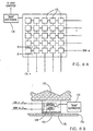
- Figs. 8A and 8B are respectively generalized and detail illustrations of apparatus for reading a charge pattern on a dielectric substrate in accordance with yet another embodiment of the present invention.
- strips 144 in the embodiment of Figs. 7A and 7B are replaced by a plurality of pixel sized conductive pads 170 which define a two-dimensionally addressable array 172 disposed adjacent a surface 174 of a dielectric substrate 176.
- an accumulator 178 is associated with each pad 170 in the array 172.
- a scanning alternating polarity charge source having precisely defined edge resolution need not be provided and may be replaced by static apparatus for supplying a uniform flow of alternating polarity charges over the entire array 172.
- Read electronics 173 measures the voltage stored in a selected accumulator 178 in accordance with the technique, described hereinabove in conjunction with Figs. 1A and 1B.
- Information from the read electronics 173 may be serially fed to a host computer (NOT SHOWN).
- Accumulators are selected for reading by common matrix addressing techniques.
- Fig. 8B illustrates a schematic arrangement for addressing a given pad 170, corresponding to a given area element or pixel on the dielectric surface 176.
- Mechanical support for the array of pads 172 is provided by a plate 179 which is typically glass.
- both accumulators 178 and drivers associated with data flip-flops can be electronically coupled to the same conductive pads.
- the read electronics 173 may be activated in a time shared manner with the write electronics.
- FIGs. 9A - 9C illustrate the operation and structure of an imaging system constructed and operated in accordance with a preferred embodiment of the present invention.
- the imaging system of Figs. 9A - 9C may constitute any suitable imaging system such as a camera or scanner.
- the illustrated embodiment preferably comprises an EAPCS 238 of the type above described in conjunction with Fig. 7A and further preferably comprises a multi-layered drum 240 having an external photoconductive layer 242, which operates as a dielectric, and an innermost supporting substrate 244. Disposed intermediate the photoconductive layer 242 and the support substrate 244 is a layer 246 incorporating a plurality of conductive bands 248.
- the supporting substrate 244 is a dielectric substrate.
- a dielectric layer 250 is required between layer 246 and substrate 244 to electrically insulate the conductive bands 248 from metal substrate 244.
- the conductive bands 248 are preferably continuously biased to a voltage +V which corresponds to voltage V set of Figs. 1A - 1B.
- an electronic reader circuit 252 schematically represented in Fig. 9C.
- the reader circuit 252 preferably comprises a plurality of accumulators 254 which correspond to accumulators 162 of Fig. 7A, a multiplexer 256 which corresponds to multiplexer 158 of Fig. 14A and read electronics 258 which correspond to read electronics 159 of Fig. 7A.
- a standard optical imaging system 259 is employed to project an image on a region 260 of the photoconductor 242, which has preferably been precharged. As a result of the image projection an electrostatic pattern corresponding to the image is created on the corresponding portion 260 of an outer surface 261 of photoconductor 242.
- the electrostatic pattern is read by applying a flow of charges to the pattern bearing region of surface 261 of the dielectric photoconductor 242, using EAPCS 238, thereby inducing a current flow representing the pattern in accordance with the read techniques above described in conjunction with Figs. 7A and 7B.
- the current flow is sensed by electronic read circuit 252.
- the surface 261 of the photoconductive layer 242 is effectively erased and simultaneously uniformly charged, thus providing precharging of the photoconductor prior to imaging by imaging system 259.
- electrostatic image generation on a portion of the surface 261 of the photoconductor 242 and reading of an electrostatic pattern from a different portion of the surface 261 of the photoconductor 242 in accordance with the present invention can occur simultaneously.
- Figs. 9A-9C is illustrated schematically and that the invention may be embodied in any suitable type of configuration, not limited to the use of drums, conductive bands and EAPCSs.
- external photoconductive layer 242 is replaced by an external dielectric layer.
- read electronics circuit 252 is replaced by write electronics as described hereinabove. It is appreciated that this alternate embodiment may comprises a cylindrical write apparatus and that the need for image source 259 is obviated.
- FIGs 10A and 10B are pictorial illustrations of an alternative embodiment of an apparatus for providing an alternating polarity charge beam having at least one defined edge.
- Apparatus 550 comprises alternating charge pool generating apparatus 552, a casing 556 and an elongate electrostatic shield 560.
- Apparatus 552 preferably comprises one or more corona wires 554 some or all of which may be dielectrically coated. Alternately, corona wires 554 may not be dielectrically coated. Each corona wire 554 is functional to receive a high AC voltage. All of the wires 554 may be biased by the same AC source (not shown). Alternately, corona wires 554 may be biased by AC sources having different amplitudes. It is appreciated that each corona wire 554 may receive a different AC voltage.
- Corona wires 554 are confined by isolating casing 556.
- casing 556 comprises a dielectric material.
- Casing 556 typically contains an elongate grounded section 558 which is partially open and wherein an ion pool is created.
- the open area of grounded section 558 may comprise a gridlike area. Alternately, the open area may comprise at least one elongate slot.
- casing 556 may further comprise an inlet through which conditioned air may flow onto corona wires 554.
- the intensity of the ion pool created at section 558 may be increased.
- electrostatic shield 560 typically comprising a grounded conductive material is placed with some spacing relative to charge pool apparatus 552. Electrostatic shield 560 may be configured as illustrated whereby charge pool apparatus 552 is partially obscured.
- apparatus 550 may serve as an elongate alternating polarity charge (EAPCS) source described hereinabove in accordance with the read and/or write techniques described hereinabove. It is further appreciated that this configuration is presented to offer an example of possible configurations for the EAPCS and is not intended to be limiting.
- EAPCS elongate alternating polarity charge
Landscapes
- Physics & Mathematics (AREA)
- General Physics & Mathematics (AREA)
- Engineering & Computer Science (AREA)
- General Engineering & Computer Science (AREA)
- Theoretical Computer Science (AREA)
- Printers Or Recording Devices Using Electromagnetic And Radiation Means (AREA)
- Facsimile Heads (AREA)
Description
- The present invention relates to apparatus and methods for non-contact printing, reading and imaging.
- There exist in the patent literature disclosures of a great number of techniques for non-contact printing and imaging. The most widely used of these techniques is electrophotography wherein an electrostatic image is optically formed on a photoconductor, which is then developed with a toner. The toner image is transferred to a substrate and fused thereon.
- An additional technique in general use is ionography, wherein an electrostatic image is formed on a dielectric substrate by firing charges directly on the substrate using an imagewise ion source.
- A technique for the transfer of electrostatic images from a photoconductor dielectric onto a dielectric substrate has also been proposed in Electrophotography by R.M. Schaffert, 2nd Edition, Focal Press, London, 1975 at pages 166 - 176 and in U.S. Patent 3,055,006. This technique, known as TESI (Transfer of Electrostatic Images) employs an imagewise optical signal to create a charge image on a photoconductor. The charge image is subsequently replicated onto a dielectric substrate by applying single polarity charges to a surface of the dielectric substrate opposite from that surface which faces the photoconductor.
- It is also known to read electrostatically a charge pattern by opposing electrodes, see EP-A-0 327 236, Fig 2, or EP-A-0 368 316, Fig 3.
- According to this invention there is provided an apparatus as claimed in
claim 1 and a method as claimed in claim 10 herein. - Preferred features of the invention are defined in the dependent claims.
- The present invention will be understood and appreciated more fully from the following detailed description, taken in conjunction with the drawings in which:
- Figs. 1A and 1B are illustrations of apparatus for reading an electrostatic charge pattern on a surface of a dielectric substrate in accordance with this invention;
- Figs. 2A, 2B and 2C are diagrams illustrating the behavior of voltages at different points on the electronic circuit of Figs. 1A and 1B;
- Figs. 3A, 3B, 3C and 3D are diagrams illustrating the operation of the apparatus of Figs. 1A and 1B at a single pixel location on the surface of the dielectric substrate;
- Fig. 4A is a schematic illustration of an arbitrary "original" charge pattern on a surface of a dielectric substrate;
- Fig. 4B is a diagram illustrating a voltage signal which results from reading the charge pattern;
- Fig. 5 is a pictorial illustration of apparatus for reading a charge pattern on a dielectric substrate;
- Figs. 6A, 6B and 6C are diagrams of various operational parameters of the apparatus of Fig. 5;
- Figs. 7A and 7B are respective generalized and side view illustrations of apparatus for reading a charge pattern on the surface of a dielectric substrate in accordance with another embodiment of the present invention ;
- Figs. 8A and 8B are respective generalized and detail illustrations of apparatus for reading a charge pattern on a dielectric substrate in accordance with yet another embodiment of the present invention;
- Figs. 9A - 9C are illustrations of the operation of an imaging system constructed and operative in accordance with a preferred embodiment of the present invention;
- Figs. 10A and 10B are pictorial illustrations of an alternative embodiment of an apparatus for providing an alternating polarity charge beam having at least one defined edge in accordance with the present invention.
-
- Reference is now made to Figs. 1A and 1B which illustrate apparatus for reading an
electrostatic charge pattern 100 on a surface of adielectric substrate 102. The dielectric substrate can be any suitable dielectric substrate and may include a photoconductor or any substrate which exhibits dielectric qualities at a given time. - The
charge pattern 100 to be read is created by any suitable technique on asurface 104 of a dielectric substrate having first and secondopposite surfaces charge pattern 100 is distributed over discrete regions (P1..PN) of the substrate. - In accordance with an embodiment of the invention, each region of the pattern is read individually using the technique described below. Each such region typically defines a pixel. Normally a two dimensional pixel distribution is envisioned. For convenience of illustration, only one dimension is illustrated in many of the drawings herein.
- As illustrated in Fig. 1A, an alternating polarity charge source (APCS) 108, which may be as mentioned hereinabove, is employed to supply a flow of charges to the region P1 of
surface 104. As the flow of charges is supplied to the region P1, a current is induced in aconductive backing 110 lyingadjacent surface 106 and a charge, corresponding to the charge originally at region P1, is accumulated, preferably bycapacitive means 112. The capacitive means is electrically coupled to theconductive backing 110 and comprises a capacitor having a capacitance of Co. - Electronic means for sensing and measuring the accumulated charge, typically including a sample and hold
device 114, are coupled to the capacitive means. Preferably the electronic means further comprises anelectronic switch 116 which, when open, causes charge to accumulate in thecapacitive means 112. When theelectronic switch 116 is closed, thecapacitive means 112 is discharged and reset. An output of the electronic means, an analog voltage Vr, is indicative of the charge at region P1 prior to the supply of charges thereto by APCS 108. The voltage Vr may be serially stored in an external digital memory device (not shown) by using an analog to digital converter. - The steps of supplying a flow of charges and then sensing the generated voltage signal may be repeated across the entire substrate resulting in serial data outputs from pixel regions P1 to Pn where n is the number of pixels on the substrate. The serial data of the different regions represents the entire pattern.
- Fig 1B illustrates an equivalent circuit corresponding to the electrical relationship of the
APCS 108, thesubstrate 102, theconductive backing 110 and the capacitive means 112. The electronicmeans comprising switch 116 and sample andhold circuit 114 may be collectively referred to as "read electronics". - Reference is now made to Figs. 2A - 2C which illustrate the behavior of voltages at different points on the electronic circuit described in Figs. 1A and 1B.
- Fig. 2A illustrates the status of the
electronic switch 116. When closed, switch 116 causes thecapacitor 112 to discharge and reset. Whenswitch 116 is open, thecapacitor 112 may accumulate charge. - Fig. 2B illustrates the effective voltage across the
capacitor 112 as a function of time. At time T1, theAPCS 108 begins to sweep over region P1 and supplies a net flow of charges to that region, inducing a current flow from theconductive backing 110 tocapacitor 112, producing accumulation of charge thereat. - This current flow continues until the net effect of the charge flow from the
APCS 108 on pixel P1 is zero. At time T2, the voltage across thecapacitor 112, Vacc, is sampled and processed by the sampling andhold circuit 114. Figure 2C graphically illustrates output voltage Vr as a function of time. - The equivalent circuit of Fig. 1B can be further employed to describe the behavior of the apparatus of Fig. 1A. The
dielectric substrate 102 is represented by capacitor Cd in Fig. 1B. The surface charge at an arbitrary pixel P1, associated with the charge pattern previously present on thesurface 104 of thesubstrate 102 is denoted, for the purposes of the discussion which follows, as Qd and the voltage Vd across the dielectric, associated with this charge is: - The
APCS 108 provides a flow of charges to thedielectric surface 102 causing charging of theaccumulator 112. This may be envisioned as the result of an equivalent current flow i across both the dielectric Cd and the capacitor Co, which representsaccumulator 112. - Consequently, the potential across the dielectric changes from Vd to Vd* where
- Simultaneously a voltage Vacc develops across capacitor Co where:
- According to the above description of the operation of the APCS, the effective flow of net charge to the pixel P1 at the dielectric surface continues until the potential resulting from both the residual charge on
surface 104 and the voltage of theconductive backing 110 at pixel P1 is effectively zero. Therefore at T2 the potential Vd* is given by - The value of Vacc is obtained by combining equations 1 - 4 where
- For a particular case where Vset is ground
- The value for Co may be determined by examining the ratio between the voltage Vd, prior to APCS charge supply, and Vacc. Since the potentials of electrostatic images are typically on the order of hundreds of volts and Vacc is desirably no more than a few volts, a typical value for Co is 100 times greater than the pixel capacitance Cd.
- It is further appreciated that since Vacc is considerably smaller than Vset, the ultimate potential across the dielectric surface is practically equal to Vset, irrespective of the previous charge Qd.
- Reference is now made to Figs. 3A - 3D. which illustrate the operation of the apparatus of Figs. 1A and 1B at a single pixel location on the surface of the
dielectric substrate 102. Fig. 3A illustrates the voltage Vd, at that same pixel location as it varies with time for a case where Vset is ground. Therefore following the sweep of the APCS of the pixel location, the voltage remaining thereat is effectively zero. - Fig. 3B illustrates, on the same time scale as that of Fig. 3A, the application of a flow of charges by the APCS to the same pixel location whereby, following application of such flow of charges, the voltage at that pixel location is zero.
- In accordance with the illustrated preferred embodiment of the invention, the flow of charges comprises an alternating polarity charge flow to the surface of the dielectric substrate. This charge flow occurs over a time span which is short relative to the time necessary to sweep the pixel dimension along a given direction of motion of the APCS. Therefore, during this time span the location of the APCS relative to the pixel location does not change considerably, and the charge flow may be represented by a stack of positive and negative charges as shown in Fig. 3B. The beginning and end of the duration of the alternating polarity charge flow are indicated in Fig. 3B respectively as T1 and T2.
- Fig. 3C is an expanded time scale illustration corresponding to Fig. 3A and illustrates with greater particularity one possible application of typical alternating charge flow to the
surface 104 of thedielectric substrate 102, which produces a change in the voltage at the pixel location onsurface 104 from the voltage at time T1 to effectively a zero voltage at time T2. The flow of charges illustrated induces a corresponding current in theconductive backing 110. The current induced in theconductive backing 110 causes a charge to be accumulated by thecapacitor 112, which is electronically coupled to theconductive backing 110. - Fig. 3D illustrates the voltage Vr, output by the read electronics, which sense and measure the charge accumulated in
capacitor 112. The voltage output by the read electronics is in direct negative proportion to the original charge at the pixel location at which the flow of charges was applied. - Referring now to Fig. 4A, there is shown schematically an arbitrary "original"
charge pattern 118 on asurface 119 of adielectric substrate 120, whichsubstrate 120 is preferably backed with aconductive backing 122. Accumulative means 123 and readelectronics 124, as described in Figs. 1A and 1B, are electronically coupled to theconductive backing 122. Also illustrated is an alternating polarity charge source (APCS) 126, of the type illustrated in Figs. 1A and 1B, which is typically capable of achieving a spatial edge accuracy consistent with a desired resolution. TheAPCS 126 is preferably moved at a constant velocity v along the surface of the dielectric substrate. Fig. 4B illustrates the voltage signal which results from reading thecharge pattern 118 in accordance with the techniques described hereinabove. - Figure 5 is a pictorial illustration of apparatus for reading a charge pattern on a dielectric substrate according to the steps described hereinabove in conjunction with Figs. 1A and 1B.
- A
charge source 138, such as an APCS which produces charges which vary in polarity as a function of time, sweeps asurface 139 of adielectric substrate 130 along an arbitrary pattern such as the up/down and sideways pattern of Fig. 5. Associated with thedielectric substrate 130 is aconductive backing 132. - In the illustrated embodiment, there is initially located on surface 139 a charge pattern which is uniformly negative above a
diagonal line 136 and is uniformly positive below the diagonal line. It is appreciated that this charge pattern may be generated by any suitable technique. - As the
charge source 138 sweeps and zeros a pixel location on thesubstrate surface 139, accumulative means 140 and readelectronics 141, in accordance with the technique described hereinabove, produce an output Vr which corresponds to the voltage previously present at that pixel location. - The operation of the apparatus of Fig. 5 may be appreciated and better understood by means of reference to Figs. 6A - 6C. Figs 6A - 6C, all of which represent events taking place along the same time scale, illustrate operational parameters of the apparatus of Fig. 5.
- Fig. 6A illustrates the voltage Vr output by the read
electronics 141 as a function of time. The time indications t1 - t6 illustrate the position of theAPCS 138 at various times. Figs. 6B and 6C illustrate the Y and X positions of theAPCS 138 as a function of time. - Reference is now made to Figs. 7A and 7B which illustrate-apparatus for reading a charge pattern on the surface of a dielectric substrate in accordance with another embodiment of the present invention. In this embodiment, an elongate alternating polarity charge source (EAPCS) 146 scans in one dimension, perpendicular to its longitudinal axis, along a
surface 148 of adielectric substrate 142, by means of a linear drive mechanism including aworm screw 150 cooperating with ascrew rider 152, fixed tosource 146. Anelectric motor 154 drives theworm screw 150. A commercially availablesynchronized encoder 156 provides position information about theEAPCS 146 to a host computer (NOT SHOWN) at any given time. - In this embodiment, a multisectional
conductive backing layer 160, typically comprising a plurality ofelongate strips 144, is associated with a surface of thedielectric substrate 142. Eachstrip 144 is associated withindividual means 162 for accumulating the charge which flows from that strip. Typically the accumulating means 162 includes a capacitor. - A
multiplexer 158 is associated with theindividual accumulators 162 and functions to select theaccumulator 162 whose output is sampled by readelectronics 159 at any given time. The readelectronics 159 measures the voltage stored in the selectedaccumulator 162 in accordance with the technique described hereinabove in conjunction with Figs. 1A and 1B. Information from the readelectronics 159 may be serially fed to a host computer (NOT SHOWN). - For read/write applications both
accumulators 162 and drivers not shown can be electronically coupled to the same conductive strips. Theread electronics 159 may be activated in a time shared manner with the write electronics. - It is appreciated that a desired twodimensional spatial resolution may be achieved by adjusting appropriate parameters. In a first dimension, the parameters to be adjusted include the width of the
elongate strips 144, the width of thegap 145 betweenadjacent strips 144 and the thickness of thedielectric layer 142. In a second dimension, the parameters include the edge definition of theEAPCS 146 and time intervals between two subsequent sampling cycles of the readelectronics 159 from the same accumulator. - Reference is now made to Figs. 8A and 8B which are respectively generalized and detail illustrations of apparatus for reading a charge pattern on a dielectric substrate in accordance with yet another embodiment of the present invention. Here, strips 144 in the embodiment of Figs. 7A and 7B are replaced by a plurality of pixel sized
conductive pads 170 which define a two-dimensionallyaddressable array 172 disposed adjacent asurface 174 of adielectric substrate 176. Preferably, anaccumulator 178 is associated with eachpad 170 in thearray 172. In this case, a scanning alternating polarity charge source having precisely defined edge resolution need not be provided and may be replaced by static apparatus for supplying a uniform flow of alternating polarity charges over theentire array 172. Readelectronics 173 measures the voltage stored in a selectedaccumulator 178 in accordance with the technique, described hereinabove in conjunction with Figs. 1A and 1B. Information from the readelectronics 173 may be serially fed to a host computer (NOT SHOWN). Accumulators are selected for reading by common matrix addressing techniques. - Fig. 8B illustrates a schematic arrangement for addressing a given
pad 170, corresponding to a given area element or pixel on thedielectric surface 176. Mechanical support for the array ofpads 172 is provided by aplate 179 which is typically glass. - For read/write applications both
accumulators 178 and drivers associated with data flip-flops (not shown) can be electronically coupled to the same conductive pads. Theread electronics 173 may be activated in a time shared manner with the write electronics. - Reference is now made to Figs. 9A - 9C which illustrate the operation and structure of an imaging system constructed and operated in accordance with a preferred embodiment of the present invention. The imaging system of Figs. 9A - 9C may constitute any suitable imaging system such as a camera or scanner.
- The illustrated embodiment preferably comprises an
EAPCS 238 of the type above described in conjunction with Fig. 7A and further preferably comprises amulti-layered drum 240 having an externalphotoconductive layer 242, which operates as a dielectric, and an innermost supportingsubstrate 244. Disposed intermediate thephotoconductive layer 242 and thesupport substrate 244 is alayer 246 incorporating a plurality ofconductive bands 248. - Preferably the supporting
substrate 244 is a dielectric substrate. In an alternative embodiment where the supportingsubstrate 244 is a metal, adielectric layer 250 is required betweenlayer 246 andsubstrate 244 to electrically insulate theconductive bands 248 frommetal substrate 244. - The
conductive bands 248 are preferably continuously biased to a voltage +V which corresponds to voltage Vset of Figs. 1A - 1B. Preferably associated withconductive bands 248 is anelectronic reader circuit 252 schematically represented in Fig. 9C. Thereader circuit 252 preferably comprises a plurality ofaccumulators 254 which correspond toaccumulators 162 of Fig. 7A, amultiplexer 256 which corresponds to multiplexer 158 of Fig. 14A and readelectronics 258 which correspond to readelectronics 159 of Fig. 7A. - A standard
optical imaging system 259 is employed to project an image on aregion 260 of thephotoconductor 242, which has preferably been precharged. As a result of the image projection an electrostatic pattern corresponding to the image is created on thecorresponding portion 260 of anouter surface 261 ofphotoconductor 242. - In the present invention, the electrostatic pattern is read by applying a flow of charges to the pattern bearing region of
surface 261 of thedielectric photoconductor 242, usingEAPCS 238, thereby inducing a current flow representing the pattern in accordance with the read techniques above described in conjunction with Figs. 7A and 7B. The current flow is sensed byelectronic read circuit 252. - Following reading of the pattern, the
surface 261 of thephotoconductive layer 242 is effectively erased and simultaneously uniformly charged, thus providing precharging of the photoconductor prior to imaging byimaging system 259. - It is appreciated that electrostatic image generation on a portion of the
surface 261 of thephotoconductor 242 and reading of an electrostatic pattern from a different portion of thesurface 261 of thephotoconductor 242 in accordance with the present invention can occur simultaneously. - It is noted that the apparatus of Figs. 9A-9C is illustrated schematically and that the invention may be embodied in any suitable type of configuration, not limited to the use of drums, conductive bands and EAPCSs.
- In accordance with an alternate embodiment of the apparatus of Figs. 9A - 9C, external
photoconductive layer 242 is replaced by an external dielectric layer. Furthermore, readelectronics circuit 252 is replaced by write electronics as described hereinabove. It is appreciated that this alternate embodiment may comprises a cylindrical write apparatus and that the need forimage source 259 is obviated. - Reference is now made to Figs 10A and 10B which are pictorial illustrations of an alternative embodiment of an apparatus for providing an alternating polarity charge beam having at least one defined edge.
-
Apparatus 550 comprises alternating chargepool generating apparatus 552, acasing 556 and an elongateelectrostatic shield 560.Apparatus 552 preferably comprises one ormore corona wires 554 some or all of which may be dielectrically coated. Alternately,corona wires 554 may not be dielectrically coated. Eachcorona wire 554 is functional to receive a high AC voltage. All of thewires 554 may be biased by the same AC source (not shown). Alternately,corona wires 554 may be biased by AC sources having different amplitudes. It is appreciated that eachcorona wire 554 may receive a different AC voltage. -
Corona wires 554 are confined by isolatingcasing 556. Typically casing 556 comprises a dielectric material. Casing 556 typically contains an elongate groundedsection 558 which is partially open and wherein an ion pool is created. - The open area of grounded
section 558 may comprise a gridlike area. Alternately, the open area may comprise at least one elongate slot. - According to an alternate embodiment of
apparatus 552, casing 556 may further comprise an inlet through which conditioned air may flow ontocorona wires 554. In this embodiment, the intensity of the ion pool created atsection 558 may be increased. - In order to achieve an ion beam which has at least one edge elongate
electrostatic shield 560 typically comprising a grounded conductive material is placed with some spacing relative to chargepool apparatus 552.Electrostatic shield 560 may be configured as illustrated wherebycharge pool apparatus 552 is partially obscured. - It is appreciated that
apparatus 550 may serve as an elongate alternating polarity charge (EAPCS) source described hereinabove in accordance with the read and/or write techniques described hereinabove. It is further appreciated that this configuration is presented to offer an example of possible configurations for the EAPCS and is not intended to be limiting. - It will be appreciated by persons skilled in the art that the present invention is not limited to what has been particularly shown and described hereinabove. Rather the scope of the present invention is defined only by the claims which follow:
Claims (14)
- Apparatus for reading an electrostatic charge pattern (100) comprising:a dielectric substrate (102) having first (106) and second (104) opposite surfaces;a conductive backing (110) operatively associated with said first surface;an information bearing charge distribution (p1-pN) defining a pattern associated with said second surface ;means (108) for applying a flow of charges to said second surface thereby converting said information bearing charge pattern to a corresponding electrical signal in said conductive backing; andmeans (112-116) coupled to said conductive backing for sensing said electrical signal and providing an electrical output representing said pattern.
- Apparatus according to claim 1,
wherein the flow of charges which is applied to the second surface of the dielectric substrate contains charges of a single polarity. - Apparatus according to claim 1,
wherein the flow of charges which is applied to the second surface of the dielectric substrate contains charges of both positive and negative polarities. - Apparatus according to claim 3,
wherein the flow of charges alternates in time between positive and negative charges. - Apparatus according to claim 1,
wherein application of said charges to the second surface is operative to generate at the first surface a voltage signal in accordance with the charge pattern on the second surface. - Apparatus according to claim 1,
wherein said means coupled to said conductive backing comprises:capacitive means 112 for receiving said electrical signal; andmeans (116,114) coupled to said capacitive means for providing spatial pattern information corresponding to said electrical signal. - Apparatus according to claim 6,
wherein said means for providing spatial pattern information comprises means (116, 114) for sensing the voltage on said capacitive means in a time domain which corresponds to a spatial domain in which the pattern is defined. - Apparatus according to claim 7,
wherein said means for sensing the voltage comprises sample and hold means (114). - Apparatus as claimed in claim 1 wherein there is provided:means (552) for applying a flow of charges to said second surface of the dielectric substrate wherein the charges flow from a generally non-imagewise source and whereby as a result of application of such charges. the second surface retains a non-visible charge pattern corresponding to the desired pattern represented by the voltage signals; andmeans (554, 560) for thereafter employing the non-visible charge pattern to provide a visible image, wherein said means for providing a flow of charges includes an ion source assembly providing edge definition and comprising:an elongate ion source (554):an elongate electrostatic shield (560) disposed about said elongate ion source and defining an elongate opening parallel to said elongate ion source. said opening including an elongate edge, which limits the spatial extent of ion pathways extending through said opening.
- A method for reading an electrostatic charge pattern including the steps of:providing a dielectric substrate having first and second opposite surfaces;operatively associating a conductive backing with said first surface;associating an information bearing charge distribution defining a pattern with said second surface;applying a flow of charges to said second surface thereby converting said information bearing charge pattern to a corresponding electrical signal in said conductive backing; andsensing said electrical signal and providing an electrical output representing said pattern.
- A method according to claim 10,
wherein the flow of charges which is applied to the second surface of the dielectric substrate contains charges of both positive and negative polarities. - A method according to claim 10, and
wherein said step of sensing includes the steps of:capacitively accumulating said electrical signal;providing spatial pattern information corresponding to said electrical signal. - A method according to the method of claim 12, and including the step of sensing the voltage corresponding to said accumulated electrical signal in a time domain which corresponds to a spatial domain in which the pattern is defined.
- A method according to claim 13,
wherein the step of sensing the voltage includes the step of sensing the voltage using sample and hold means.
Applications Claiming Priority (9)
| Application Number | Priority Date | Filing Date | Title |
|---|---|---|---|
| US07/697,166 US5157423A (en) | 1991-05-08 | 1991-05-08 | Apparatus for pattern generation on a dielectric substrate |
| US697166 | 1991-05-08 | ||
| US766691 | 1991-09-27 | ||
| US07/766,691 US5289214A (en) | 1991-05-08 | 1991-09-27 | Apparatus for information transfer including a dielectric element and generally non-imagewise charge service |
| IL10069492 | 1992-01-17 | ||
| IL10069492A IL100694A (en) | 1992-01-17 | 1992-01-17 | Apparatus for information transfer |
| IL100961A IL100961A0 (en) | 1992-02-14 | 1992-02-14 | Apparatus for information transfer |
| IL10096192 | 1992-02-14 | ||
| EP92912165A EP0538454B1 (en) | 1991-05-08 | 1992-05-08 | Apparatus for information transfer |
Related Parent Applications (2)
| Application Number | Title | Priority Date | Filing Date |
|---|---|---|---|
| EP92912165A Division EP0538454B1 (en) | 1991-05-08 | 1992-05-08 | Apparatus for information transfer |
| EP92912165.5 Division | 1992-11-20 |
Publications (3)
| Publication Number | Publication Date |
|---|---|
| EP0769732A2 EP0769732A2 (en) | 1997-04-23 |
| EP0769732A3 EP0769732A3 (en) | 1997-07-09 |
| EP0769732B1 true EP0769732B1 (en) | 2001-12-05 |
Family
ID=27513996
Family Applications (1)
| Application Number | Title | Priority Date | Filing Date |
|---|---|---|---|
| EP96119389A Expired - Lifetime EP0769732B1 (en) | 1991-05-08 | 1992-05-08 | Apparatus for information transfer |
Country Status (2)
| Country | Link |
|---|---|
| EP (1) | EP0769732B1 (en) |
| KR (1) | KR930702658A (en) |
Family Cites Families (7)
| Publication number | Priority date | Publication date | Assignee | Title |
|---|---|---|---|---|
| NL273832A (en) | 1961-01-24 | |||
| US4155093A (en) * | 1977-08-12 | 1979-05-15 | Dennison Manufacturing Company | Method and apparatus for generating charged particles |
| US4409604A (en) * | 1981-01-05 | 1983-10-11 | Dennison Manufacturing Company | Electrostatic imaging device |
| ATE113746T1 (en) | 1986-06-03 | 1994-11-15 | Cubital Ltd | DEVICE FOR DEVELOPING THREE-DIMENSIONAL MODELS. |
| EP0327236B1 (en) * | 1988-01-24 | 1994-11-30 | Victor Company Of Japan, Limited | Image pickup apparatus |
| US5003402A (en) * | 1988-11-10 | 1991-03-26 | Victor Company Of Japan, Ltd. | Apparatus for recording and reproducing charge latent image |
| JPH02143778A (en) * | 1988-11-25 | 1990-06-01 | Victor Co Of Japan Ltd | Read system for electric charge latent image |
-
1992
- 1992-05-08 KR KR1019930700059A patent/KR930702658A/en not_active Ceased
- 1992-05-08 EP EP96119389A patent/EP0769732B1/en not_active Expired - Lifetime
Also Published As
| Publication number | Publication date |
|---|---|
| EP0769732A3 (en) | 1997-07-09 |
| KR930702658A (en) | 1993-09-09 |
| EP0769732A2 (en) | 1997-04-23 |
Similar Documents
| Publication | Publication Date | Title |
|---|---|---|
| US5289214A (en) | Apparatus for information transfer including a dielectric element and generally non-imagewise charge service | |
| US5268569A (en) | Imaging system having optimized electrode geometry and processing | |
| CA1150946A (en) | Method and apparatus for electrically biasing developing electrode of electrophotographic device | |
| JP3005130B2 (en) | Charging device, image forming apparatus, and process cartridge | |
| US5640190A (en) | Non-impact printer with evenness control | |
| JPH11288152A (en) | Image forming device for digital xerography | |
| EP0751440B1 (en) | Image forming apparatus | |
| US4546364A (en) | Head for electrostatic recording | |
| US4868907A (en) | Self-biased scorotron grid power supply and electrostatic voltmeter operable therefrom | |
| AU672987B2 (en) | Imaging system and device having a simplified electrode design | |
| US6043830A (en) | Apparatus for pattern generation on a dielectric substrate | |
| US4620203A (en) | Electrostatic image forming apparatus using field effect transistors | |
| US4559564A (en) | Two-dimensional image reader | |
| US4447821A (en) | Method and apparatus of electrostatic recording | |
| US3638110A (en) | Device for measuring charge on a material by converting into electrical signals the frictional forces caused by the charge | |
| US4541017A (en) | Apparatus for contact-free measurement of electrical charge images generated by electro-radiographic recording methods | |
| EP0667565A2 (en) | Apparatus and method for pattern generation on a dielectric substrate | |
| EP0769732A2 (en) | Apparatus for information transfer | |
| US5563688A (en) | Charging device for charging in one of a plurality of predefined image areas on a surface of an imaging member | |
| EP0538454A1 (en) | DATA TRANSFER DEVICE. | |
| JPS5941346B2 (en) | 2D photoelectric conversion device | |
| Bartscher et al. | Comparison of the electric fields of electrophotography and contact electrography | |
| IL100694A (en) | Apparatus for information transfer | |
| US5742051A (en) | Micro sized ion generating device | |
| EP0706891A2 (en) | Apparatus and methods for non impact imaging and digital printing |
Legal Events
| Date | Code | Title | Description |
|---|---|---|---|
| PUAI | Public reference made under article 153(3) epc to a published international application that has entered the european phase |
Free format text: ORIGINAL CODE: 0009012 |
|
| AC | Divisional application: reference to earlier application |
Ref document number: 538454 Country of ref document: EP |
|
| AK | Designated contracting states |
Kind code of ref document: A2 Designated state(s): AT BE CH DE DK ES FR GB GR IT LI LU MC NL SE |
|
| PUAL | Search report despatched |
Free format text: ORIGINAL CODE: 0009013 |
|
| AK | Designated contracting states |
Kind code of ref document: A3 Designated state(s): AT BE CH DE DK ES FR GB GR IT LI LU MC NL SE |
|
| RHK1 | Main classification (correction) |
Ipc: H04N 5/30 |
|
| 17P | Request for examination filed |
Effective date: 19980107 |
|
| 17Q | First examination report despatched |
Effective date: 19990804 |
|
| GRAG | Despatch of communication of intention to grant |
Free format text: ORIGINAL CODE: EPIDOS AGRA |
|
| GRAG | Despatch of communication of intention to grant |
Free format text: ORIGINAL CODE: EPIDOS AGRA |
|
| GRAH | Despatch of communication of intention to grant a patent |
Free format text: ORIGINAL CODE: EPIDOS IGRA |
|
| GRAH | Despatch of communication of intention to grant a patent |
Free format text: ORIGINAL CODE: EPIDOS IGRA |
|
| GRAA | (expected) grant |
Free format text: ORIGINAL CODE: 0009210 |
|
| AC | Divisional application: reference to earlier application |
Ref document number: 538454 Country of ref document: EP |
|
| AK | Designated contracting states |
Kind code of ref document: B1 Designated state(s): AT BE CH DE DK ES FR GB GR IT LI LU MC NL SE |
|
| PG25 | Lapsed in a contracting state [announced via postgrant information from national office to epo] |
Ref country code: NL Free format text: LAPSE BECAUSE OF FAILURE TO SUBMIT A TRANSLATION OF THE DESCRIPTION OR TO PAY THE FEE WITHIN THE PRESCRIBED TIME-LIMIT Effective date: 20011205 Ref country code: LI Free format text: LAPSE BECAUSE OF FAILURE TO SUBMIT A TRANSLATION OF THE DESCRIPTION OR TO PAY THE FEE WITHIN THE PRESCRIBED TIME-LIMIT Effective date: 20011205 Ref country code: IT Free format text: LAPSE BECAUSE OF FAILURE TO SUBMIT A TRANSLATION OF THE DESCRIPTION OR TO PAY THE FEE WITHIN THE PRESCRIBED TIME-LIMIT;WARNING: LAPSES OF ITALIAN PATENTS WITH EFFECTIVE DATE BEFORE 2007 MAY HAVE OCCURRED AT ANY TIME BEFORE 2007. THE CORRECT EFFECTIVE DATE MAY BE DIFFERENT FROM THE ONE RECORDED. Effective date: 20011205 Ref country code: GR Free format text: LAPSE BECAUSE OF FAILURE TO SUBMIT A TRANSLATION OF THE DESCRIPTION OR TO PAY THE FEE WITHIN THE PRESCRIBED TIME-LIMIT Effective date: 20011205 Ref country code: FR Free format text: LAPSE BECAUSE OF FAILURE TO SUBMIT A TRANSLATION OF THE DESCRIPTION OR TO PAY THE FEE WITHIN THE PRESCRIBED TIME-LIMIT Effective date: 20011205 Ref country code: CH Free format text: LAPSE BECAUSE OF FAILURE TO SUBMIT A TRANSLATION OF THE DESCRIPTION OR TO PAY THE FEE WITHIN THE PRESCRIBED TIME-LIMIT Effective date: 20011205 Ref country code: BE Free format text: LAPSE BECAUSE OF FAILURE TO SUBMIT A TRANSLATION OF THE DESCRIPTION OR TO PAY THE FEE WITHIN THE PRESCRIBED TIME-LIMIT Effective date: 20011205 Ref country code: AT Free format text: LAPSE BECAUSE OF FAILURE TO SUBMIT A TRANSLATION OF THE DESCRIPTION OR TO PAY THE FEE WITHIN THE PRESCRIBED TIME-LIMIT Effective date: 20011205 |
|
| REF | Corresponds to: |
Ref document number: 210353 Country of ref document: AT Date of ref document: 20011215 Kind code of ref document: T |
|
| REG | Reference to a national code |
Ref country code: CH Ref legal event code: EP |
|
| REG | Reference to a national code |
Ref country code: GB Ref legal event code: IF02 |
|
| REF | Corresponds to: |
Ref document number: 69232275 Country of ref document: DE Date of ref document: 20020117 |
|
| PG25 | Lapsed in a contracting state [announced via postgrant information from national office to epo] |
Ref country code: SE Free format text: LAPSE BECAUSE OF FAILURE TO SUBMIT A TRANSLATION OF THE DESCRIPTION OR TO PAY THE FEE WITHIN THE PRESCRIBED TIME-LIMIT Effective date: 20020305 Ref country code: DK Free format text: LAPSE BECAUSE OF FAILURE TO SUBMIT A TRANSLATION OF THE DESCRIPTION OR TO PAY THE FEE WITHIN THE PRESCRIBED TIME-LIMIT Effective date: 20020305 |
|
| PG25 | Lapsed in a contracting state [announced via postgrant information from national office to epo] |
Ref country code: DE Free format text: LAPSE BECAUSE OF FAILURE TO SUBMIT A TRANSLATION OF THE DESCRIPTION OR TO PAY THE FEE WITHIN THE PRESCRIBED TIME-LIMIT Effective date: 20020306 |
|
| NLV1 | Nl: lapsed or annulled due to failure to fulfill the requirements of art. 29p and 29m of the patents act | ||
| PG25 | Lapsed in a contracting state [announced via postgrant information from national office to epo] |
Ref country code: MC Free format text: LAPSE BECAUSE OF NON-PAYMENT OF DUE FEES Effective date: 20020508 Ref country code: LU Free format text: LAPSE BECAUSE OF NON-PAYMENT OF DUE FEES Effective date: 20020508 Ref country code: GB Free format text: LAPSE BECAUSE OF NON-PAYMENT OF DUE FEES Effective date: 20020508 |
|
| REG | Reference to a national code |
Ref country code: CH Ref legal event code: PL |
|
| PG25 | Lapsed in a contracting state [announced via postgrant information from national office to epo] |
Ref country code: ES Free format text: LAPSE BECAUSE OF FAILURE TO SUBMIT A TRANSLATION OF THE DESCRIPTION OR TO PAY THE FEE WITHIN THE PRESCRIBED TIME-LIMIT Effective date: 20020627 |
|
| PLBE | No opposition filed within time limit |
Free format text: ORIGINAL CODE: 0009261 |
|
| STAA | Information on the status of an ep patent application or granted ep patent |
Free format text: STATUS: NO OPPOSITION FILED WITHIN TIME LIMIT |
|
| EN | Fr: translation not filed | ||
| 26N | No opposition filed | ||
| GBPC | Gb: european patent ceased through non-payment of renewal fee |
Effective date: 20020508 |