EP0766501B1 - Discharging and dust removing method and apparatus - Google Patents
Discharging and dust removing method and apparatus Download PDFInfo
- Publication number
- EP0766501B1 EP0766501B1 EP19950115076 EP95115076A EP0766501B1 EP 0766501 B1 EP0766501 B1 EP 0766501B1 EP 19950115076 EP19950115076 EP 19950115076 EP 95115076 A EP95115076 A EP 95115076A EP 0766501 B1 EP0766501 B1 EP 0766501B1
- Authority
- EP
- European Patent Office
- Prior art keywords
- positive
- discharging
- negative
- working object
- electrode apparatus
- Prior art date
- Legal status (The legal status is an assumption and is not a legal conclusion. Google has not performed a legal analysis and makes no representation as to the accuracy of the status listed.)
- Expired - Lifetime
Links
- 238000007599 discharging Methods 0.000 title claims description 272
- 239000000428 dust Substances 0.000 title claims description 37
- 238000000034 method Methods 0.000 title claims description 24
- 150000002500 ions Chemical class 0.000 claims description 251
- 239000002184 metal Substances 0.000 claims description 6
- 239000002985 plastic film Substances 0.000 description 19
- 229920006255 plastic film Polymers 0.000 description 19
- 239000000843 powder Substances 0.000 description 9
- 238000004804 winding Methods 0.000 description 9
- 238000004519 manufacturing process Methods 0.000 description 7
- 239000003990 capacitor Substances 0.000 description 6
- 230000009471 action Effects 0.000 description 5
- 238000010276 construction Methods 0.000 description 5
- 238000010586 diagram Methods 0.000 description 5
- 230000008878 coupling Effects 0.000 description 4
- 238000010168 coupling process Methods 0.000 description 4
- 238000005859 coupling reaction Methods 0.000 description 4
- 239000004033 plastic Substances 0.000 description 4
- 238000004299 exfoliation Methods 0.000 description 3
- 238000005259 measurement Methods 0.000 description 3
- 238000012986 modification Methods 0.000 description 3
- 230000004048 modification Effects 0.000 description 3
- 230000007935 neutral effect Effects 0.000 description 3
- 239000000919 ceramic Substances 0.000 description 2
- 239000011248 coating agent Substances 0.000 description 2
- 239000004020 conductor Substances 0.000 description 2
- 230000008030 elimination Effects 0.000 description 2
- 238000003379 elimination reaction Methods 0.000 description 2
- 239000011521 glass Substances 0.000 description 2
- 239000004973 liquid crystal related substance Substances 0.000 description 2
- 239000000696 magnetic material Substances 0.000 description 2
- 239000000463 material Substances 0.000 description 2
- 230000010355 oscillation Effects 0.000 description 2
- 238000007639 printing Methods 0.000 description 2
- 239000011347 resin Substances 0.000 description 2
- 229920005989 resin Polymers 0.000 description 2
- 241001176668 Duck hepatitis virus 2 Species 0.000 description 1
- 230000008859 change Effects 0.000 description 1
- 238000006243 chemical reaction Methods 0.000 description 1
- 230000006866 deterioration Effects 0.000 description 1
- 230000000694 effects Effects 0.000 description 1
- 230000005684 electric field Effects 0.000 description 1
- 238000005421 electrostatic potential Methods 0.000 description 1
- 239000010419 fine particle Substances 0.000 description 1
- 239000012212 insulator Substances 0.000 description 1
- 238000006386 neutralization reaction Methods 0.000 description 1
- 239000002245 particle Substances 0.000 description 1
- 238000005192 partition Methods 0.000 description 1
- 230000008569 process Effects 0.000 description 1
- 230000004044 response Effects 0.000 description 1
- 230000001360 synchronised effect Effects 0.000 description 1
Images










Classifications
-
- H—ELECTRICITY
- H05—ELECTRIC TECHNIQUES NOT OTHERWISE PROVIDED FOR
- H05F—STATIC ELECTRICITY; NATURALLY-OCCURRING ELECTRICITY
- H05F3/00—Carrying-off electrostatic charges
- H05F3/04—Carrying-off electrostatic charges by means of spark gaps or other discharge devices
Definitions
- This invention relates to a discharging and dust removing method and a discharging and dust removing apparatus for removing electric charge and dust from a working object in the form of an electric insulating member such as a plastic film, a plastic plate, a plastic card or a paper sheet or web while it is travelling.
- an electric insulating member such as a plastic film, a plastic plate, a plastic card or a paper sheet or web while it is travelling.
- a potential and a polarity of residual electrostatic charge of the travelling object after completion of such high speed discharging processing are detected by means of a potential detector, and the DC discharger is automatically controlled in response to the thus detected potential and polarity so that it may cause DC corona discharging, which has the opposite polarity to that of the residual charge and is to cancel the residual potential, to occur from the DC discharger to remove the residual charge by neutralization.
- FIG. 8 illustrates an example of such invisible charge pattern which was made visible by scattering toner powder (black fine particles) of the negative polarity, which is normally used with a copying machine or the like, on a surface of a plastic film immediately after exfoliated from a roller so as to cause the toner powder to directly stick to the surface of the plastic film electrostatically and then transferring the sticking toner powder image, using a copying machine, to a paper sheet to obtain the figure shown in FIG. 8.
- Black portions to which toner powder stuck were positively charged portions while bright portions to which no toner powder stuck were negatively charged portions, and the intensity of the black color represents the magnitude of the electrostatic potential there.
- a polarity and a potential of charge are estimated from a result of such macroscopic measurement as described above, and charging conditions are decided uniformly in accordance with the thus estimated polarity and potential of charge (a voltage to be applied to a discharging electrode and so forth are set), and then positive and negative ions from a discharger positioned in a spaced relationship from a film are merely irradiated one-sidedly toward one face of the film.
- the opposite face of the film is left as an open face free from a grounding member or the like.
- Such situations are not unique to those products wherein a plastic material is employed, but similarly apply to those products wherein a glass plate is employed (for example, a glass base plate for a liquid crystal display or the like).
- the nearest prior art document FR-A-1 547 907 discloses a discharging apparatus which comprises an ion attracting electrode apparatus having a face extending in a travelling direction of a working piece and a perpendicular direction.
- the ion attracting electrode apparatus is a specialised form of an ion attracting apparatus because the apparatus itself generates ions. If positive ions are generated, the negative ions on the opposite side are attracted and vice versa.
- the discharging apparatus further comprises a positive and negative ion producing discharging electrode apparatus which is arranged opposite to the ion attracting apparatus with a distance allowing the free passage of the working object.
- a high voltage AC power source is connected to the ion producing apparatus and another high AC voltage is applied to the ion attracting device. The two AC voltages are synchronised with each other having opposite polarities.
- a discharging method wherein positive and negative ions are irradiated upon a travelling working object to discharge the working object, comprising the steps of passing the working object between a positive and negative ion producing discharging electrode apparatus and an ion attracting electrode apparatus disposed in an opposing relationship to the positive and negative ion producing discharging electrode apparatus and having a face which extends in a travelling direction of the working object and a perpendicular direction, applying, while the working object passes between the positive and negative ion producing discharging electrode apparatus and the ion attracting electrode apparatus, high positive and negative voltages alternately to the positive and negative ion producing discharging electrode apparatus to alternately produce positive and negative ions, and simultaneously applying another high AC voltage having a higher frequency than the above-mentioned voltage to the ion attracting electrode apparatus to induce positive and negative potentials in the working object so as to attract the positive and negative ions produced by the positive and negative ion producing discharging electrode apparatus by the induced potentials of the working object.
- a discharging apparatus comprising an ion attracting electrode apparatus having a face extending in a travelling direction of a travelling working object and a perpendicular direction, a positive and negative ion producing discharging electrode apparatus opposed to the ion attracting electrode apparatus with a distance left therebetween sufficient to allow the working object to pass therebetween, and a power source apparatus for applving high pcsitive and negative voltages alternately to the positive and negative ion producing discharging electrode apparatus to produce positive and negative ions alternately and simultaneously applying to the ion attracting electrode apparatus another high AC voltage having a higher frequency than the above-mentioned voltages applied to the positive and negative ion producing discharging electrode apparatus.
- positive and negative ions are produced from a plurality of positive and negative ion producing discharging electrodes of the positive and negative ion producing discharging electrode apparatus disposed parallelly in the travelling direction of the working object and are irradiated upon the working object so as to repetitively perform discharging of the working object.
- the ion attracting electrode apparatus may include a single ion attracting electrode provided commonly to all of the positive and negative ion producing discharging electrodes or a plurality of ion attracting electrodes individually provided corresponding to the positive and negative on producing discharging electrodes.
- the positive and negative ions produced by the positive and negative ion producing discharging electrode apparatus are not attracted to the working object when the polarities thereof are same as those of the potentials induced in the working object, but when the polarities are opposite to each other, the positive and negative ions are attracted to the working object by a Coulomb force. Since the polarities of the potentials induced in the working object vary in accordance with the period of the high ac voltage applied to the ion attracting electrode apparatus, the ions from the positive and negative ion producing discharging electrode apparatus are, whether they are positive ions or negative ions, acted upon directly by a Coulomb force from the working object and positively attracted to and irradiated upon the surface of the working object.
- the voltage applied to the ion attracting electrode apparatus is a high ac voltage which exhibits a periodical variation between positive and negative values, such a situation that the ion attracting electrode apparatus attracts the working object itself to obstruct the travelling of the working object does not occur.
- Such discharge unevenness which appears macroscopically can be eliminated more effectively by constructing the positive and negative ion producing discharging electrode apparatus such that the discharging actions by the plurality of positive and negative ion producing discharging electrodes gradually decrease toward the travelling direction of the working object or by constructing, where the ion attracting electrode apparatus includes a plurality of ion attracting electrodes individually provided corresponding to the positive and negative ion producing discharging electrodes, the ion attracting electrode apparatus such that the voltages to be applied to the ion attracting electrodes gradually decrease toward the travelling direction of the working object.
- Such elimination of macroscopic discharge unevenness can be promoted by employing, as a next auxiliary step, weak DC discharging by a DC discharger and/or weak AC discharging by an AC discharger.
- the ion attracting electrode apparatus may be in the form of a plate or a roller which rotates to guide the working object. Where a metal roller is employed, a dielectric layer is formed on the surface of the metal roller in order to produce an electrostatic capacitor between the metal roller and the working object and in order to prevent spark discharge.
- one of the positive and negative ion producing discharging electrode apparatus and the ion attracting electrode apparatus is disposed for movement toward and away from the working object so that the distance between the positive and negative ion producing discharging electrode apparatus and the ion attracting electrode apparatus may be varied.
- an air shower dust removing unit which includes an air jetting section for jetting air to the working object and an air sucking section for sucking the air jetted from the air jetting section.
- FIG. 1 there is shown a general construction of an entire discharging and dust removing apparatus to which the present invention is applied.
- a plastic film (hereinafter referred to merely as film) 1 which is an object of working is fed in the rightward direction in FIG. 1 under the guidance of a guide roller 8.
- the film 1 is first discharged at a discharging station A, and then dust is removed from the film 1 at a dust removing station B.
- a plurality of positive and negative ion producing discharging electrodes 3 are disposed in an opposing relationship to a common ion attracting electrode 2 to construct a discharging gate section 9.
- the film 1 is discharged at a plurality of stages between the positive and negative ion producing discharging electrodes 3 and the ion attracting electrode 2 in such a manner as hereinafter described while it passes the discharging gate section 9.
- Each of the discharging electrodes 3 extends in a widthwise direction of the film 1 and has a length greater than the widthwise dimension of the film 1. While discharging electrodes of various structures can be employed for the discharging electrodes 3, a discharging electrode which includes a large number of discharging needles is economically employed for the discharging electrodes 3.
- An exemplary one of existing discharging electrodes of the type just mentioned is shown in FIG. 5 (bottom plan view) and FIG. 6. Referring to FIGS.
- the positive discharging electrode 3 shown includes a large number of discharging needles 10 individually planted separately from each other on a large number of cores 11 each formed from a ceramic dielectric member or a ceramic resistor member so as to establish capacitive couplings or resistive couplings which are separate from each other.
- the cores 11 are fitted one by one in a large number of holes of a printed circuit board 12, and the cores 11 and the printed circuit board 12 are embedded in an insulating molded member 14 in a resin casing 13 such that the discharging needles 10 are partially projected from the surface of the insulating molded member 14 in a spaced relationship from each other at fixed distances in a longitudinal direction of the resin casing 13 (in the widthwise direction of the film 1).
- each of the discharging electrodes 3 can be used also as a single independent discharger.
- the discharging electrodes 3 have a length greater than the width of the film 1.
- a plurality of such discharging electrodes 3 are employed and arranged parallelly in a spaced relationship from each other in the travelling direction (longitudinal direction) of the film 1 and in a spaced relationship by a small distance from a face (upper face) of the film 1.
- a high AC voltage HV1 is applied from a high AC voltage power source AC at a time to the discharging electrodes 3.
- the distance between the discharging electrodes 3 is adjusted in accordance with the travelling speed of the film 1.
- the discharging electrodes 3 are held on a common holder 15 and can be moved (adjusted in position) toward and away from the film 1 by a pair of linear motion actuators 16 such as air cylinders.
- the ion attracting electrode 2 is formed from a single plate such as a conductive metal plate having a flat face opposing commonly to all of the discharging electrodes 3 with regard to both of the travelling direction and the widthwise direction of the film 1, and is disposed such that it does not contact with the film 1.
- a high AC voltage HV2 having a phase opposite to that of the high AC voltage HV1 to be applied to the discharging electrodes 3 is applied to the ion attracting electrode 2 from the high AC voltage power source AC.
- the ion attracting electrode 2 is supported on a pair of linear motion actuators 22 such as air cylinders by way of respective insulators 21 such that it can be moved (adjusted in position) toward and away from the film 1.
- FIG. 3 An equivalent circuit in this instance is shown in FIG. 3.
- reference character 7 denotes a grounding electrode for the positive and negative ion producing discharging electrodes 3
- C denotes an electrostatic capacitor formed between the ion attracting electrode 2 and the film 1.
- positive ion producing electrodes 3a for producing positive ions and negative ion producing electrodes 3b for producing negative ions may be provided as (or in place of) the positive and negative ion producing discharging electrodes 3 such that high positive and negative DC voltages DHV1 and DHV2 are applied to the positive ion producing electrodes 3a and the negative ion producing electrodes 3b, respectively, to produce positive and negative ions.
- An equivalent circuit in this instance is shown in FIG. 4.
- the ion attracting electrode 2 since the ion attracting electrode 2 has the face which extends in the travelling direction and the widthwise direction of the film 1, local unevenness does not occur with the ion attracting force of the ion attracting electrode 2 and the ion attracting electrode 2 can attract positive and negative ions equally. Consequently, the ion attracting electrode 2 microscopically presents minimized discharge unevenness.
- FIG. 9 shows a condition wherein toner powder is scattered in a similar manner as in the case of FIG. 8 on the face of the film 1 immediately after it passes the discharging gate section 9 (at the position 2 ⁇ in FIG. 1).
- An area N adjacent one side edge of the face of the film 1 shown in FIG. 9 is a non-discharged area which has been masked so as not to undergo discharging processing, and the travelling direction of the film 1 is indicated by an arrow mark in FIG. 9.
- the area of the face of the film 1 which has been discharged by the discharging gate section 9 does not exhibit such a complicated charge pattern as is exhibited on the non-discharged area N, but instead exhibits a plurality of thin white and black lateral stripes appearing alternately like waves in the travelling direction of the film 1 such that they extend in the widthwise direction of the film 1.
- the amounts of positive and negative ions to be produced by the positive and negative ion producing discharging electrodes 3 vary in accordance with the frequency of the high AC voltage HV1 to be applied to the positive and negative ion producing discharging electrodes 3. Therefore, where the frequency is approximately equal to or around a frequency of a commercial AC power supply (50 Hz or 60 Hz in Japan), the period of the variation of the amount of ions to be produced is so long that, if the travelling speed of the film 1 is low, the film 1 is discharged unevenly.
- the frequency of the high AC voltage HV2 to be applied to the ion attracting electrode 2 is set higher than the frequency of the high AC voltage HV1 to be applied to the discharging electrodes 3 so that such discharge unevenness caused by the variation of ions to be produced with respect to time can be reduced.
- the discharging and dust removing apparatus further includes a negative ion producing DC discharger 4, a positive ion producing DC discharger 5 and an AC discharger 6 arranged in this order subsequently to the discharging gate section 9 in the travelling direction of the film 1.
- a high negative DC voltage is applied from a high Dc voltage power source DC1 to the negative ion producing DC discharger 4 which a high positive DC voltage is applied from another high DC voltage power source DC2 to the positive ion producing DC discharger 5, and a high AC voltage is applied from a high AC voltage power source AC3 to the AC discharger 6.
- Such an AC discharger as shown in FIGS. 5 and 6 may be used for the AC discharger 6.
- a known DC discharger which employs a large number of discharging needles can be employed for the DC dischargers 4 and 5, and no special discharger need not be employed.
- the DC dischargers 4 and 5 and the AC discharger 6 are disposed such that the distances thereof to the film 1 are generally set greater than that of the discharging electrodes 3 of the discharging gate section 9 in order to make the discharging capacity to the film 1 lower than that of the discharging electrodes 3 and besides the distances thereof to the film 1 increase stepwise in the travelling direction of the film 1 in order to gradually decrease the discharging force to act upon the film 1.
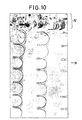
- FIG. 10 shows a condition wherein toner powder is scattered in a similar manner as described hereinabove on the face of the film 1 after it has undergone the discharging processing just described (at the position 3 ⁇ in FIG. 1). In FIG. 10, the film 1 exhibits no such wave-like charged portions as appear in FIG.
- FIG. 11 shows a condition wherein toner powder is scattered on the face of the film 1 after it has undergone the discharging processing with positive ions (at the position 4 ⁇ in FIG. 1).
- FIG. 11 only a little thin white-black thick-thin uneven pattern remains on the face of FIG. 1.
- the non-discharged area N the complicated charge pattern still remains.
- FIG. 12 shows a condition wherein toner powder is scattered on the face of the film 1 after it has undergone the discharging processing with positive and negative ions (at the position 5 ⁇ in FIG. 1).
- FIG. 12 no white-black thick-thin uneven pattern can be seen on the face of the film 1.
- the complicated charge pattern remains to the last in the non-discharged area N.
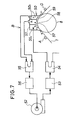
- the dust removing station B includes an air shower dust removing unit 50 located above the guide roller 8.
- the air shower dust removing unit 50 includes a casing 51 in which an air jetting section 50a and a pair of air sucking sections 50b are defined by a pair of partitions. Air jetted from the air jetting section 50a hits upon and is reflected from the film 1 on the guide roller 8 and is then sucked into the two air sucking sections 50b. Consequently, dust or some other foreign particles sticking to the film 1 are compulsorily removed from the face of the film 1 and collected by the air shower dust removing unit 50. In this instance, dust or the like is removed thoroughly from the film 1 since it has been discharged thoroughly to such a degree that it exhibits no charge pattern.
- the dust removing station B is particularly shown in FIG. 7.
- air from a blower 52 is forwarded into the air jetting section 50a of the air shower dust removing unit 50 by way of a forwarding side filter 53 and a forwarding side damper 54, and air sucked into the air sucking sections 50b is circulated back into the blower 52 by way of a sucking side damper 55 and a sucking side filter 56 by a sucking action of the blower 52.
- a nozzle 57 is provided for the air jetting section 50a such that it jets air obliquely toward the film 1 which travels on the surface of the guide roller 8.
- a small sucking opening 58 is provided at an air sucking portion of one of the air sucking sections 50b which is located adjacent the air jetting section 50a while a large sucking opening 59 is provided at an air sucking portion of the other air sucking sections 50b.
- reference character D denotes an auxiliary discharging station for discharging the film 1 after exfoliated from the guide roller 8.
- the auxiliary discharging station D may have a partially or entirely same construction as the discharging station A described hereinabove.
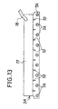
- the multiple AC discharger 3A includes a plurality of rows of discharging needles 10 disposed parallelly in a spaced relationship from each other in the travelling direction of the film 1 on an insulating holder 17 in the form of a plate such that they project from the insulating holder 17.
- Each of the rows of the discharging needles 10 includes a large number of discharging needles 10 disposed in a predetermined spaced relationship from each other in the widthwise direction of the film 1.
- the multiple AC discharger 3A further includes a plurality of grounding electrode bars 7A mounted on the insulating holder 17 such that they extend in parallel to each other and are positioned on the opposite sides of the individual rows of the discharging needles 10.
- a high tension cable 18 is led out from the insulating holder 17 so that a high AC voltage can be applied at a time to all of the discharging needles 10 by way of the high tension cable 18.
- all of the grounding electrode bars 7A can be grounded by way of a conductor plate 19 provided on the insulating holder 17 and a grounding cable 20 connected to the conductor plate 19. It is to be noted that, where the multiple AC discharger 3A shown in FIGS. 13 and 14 is employed, the ion attracting electrode 2 is formed such that it has a face opposed commonly to all of the rows of the discharging needles 10.
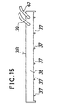
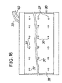
- FIGS. 15 and 16 show another multiple DC discharger 3B of the positive and negative ion simultaneous production type which can be employed in place of the discharging electrodes 3 of the discharging gate section 9.
- the multiple DC discharger 3B includes a large number of discharging needles 37 disposed in a plurality of parallel rows in a spaced relationship from each other in the travelling direction of the film 1 on an insulating holder 38 in the form of a plate and disposed, in each of the rows, in a predetermined spaced relationship from each other in the widthwise direction of the film 1.
- the discharging needles 37 are disposed such that a positive discharging needle and a negative discharging needle appear alternately in each row and between each adjacent rows as seen in FIG. 16. Or else, the discharging needles 37 may be disposed such that a row in which only positive discharging needles are arranged and another row in which only negative discharging needles are arranged appear alternately in the travelling direction of the film 1. It is to be noted that reference numerals 39 and 40 in FIGS. 15 and 16 denote high voltage cables for supplying high positive and negative dc voltages, respectively.
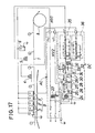
- the high AC voltage power source AC shown includes a transformer 23 for stepping up an AC voltage from a commercial AC power supply.
- One of a pair of positive and negative taps of the secondary winding of the transformer 23 is connected to all of the discharging electrodes 3 arranged in such a manner as described hereinabove while the other tap is connected to the ion attracting electrode 2.
- the high AC voltages HV1 and HV2 are applied at a time to the discharging electrodes 3 and the ion attracting electrode 2, respectively.
- the common ion attracting electrode 2 in the form of a plate is inclined, in the arrangement shown in FIG. 17, downwardly toward the travelling direction of the film 1 so that the ion attracting force to the discharging electrodes 3 may gradually decrease as the film 1 travels.
- Such downwardly inclined arrangement allows efficient elimination of macroscopic discharging unevenness.
- a high DC voltage power source apparatus DC converts the AC voltage from the commercial AC power supply into a dropped DC voltage by means of an AC to DC conversion section 26 which includes a transformer 24, a diode 25 and so forth.
- the DC voltage is supplied to a constant voltage IC circuit 27, and an AC voltage adjusted arbitrarily by a variable resistor 28 is output from an output terminal of the constant voltage IC circuit 27. Then, the thus adjusted DC voltage is smoothed by a pair of capacitors 29 and 30 and then applied to a high frequency oscillating circuit 31.
- the high frequency oscillating circuit 31 is connected to the primary winding of a high frequency transformer 32.
- a starting transistor 33 is turned on, and consequently, the high frequency oscillating circuit 31 oscillates a high frequency wave by its self-excited oscillation.
- a high AC voltage is obtained from the secondary winding of the high frequency oscillating circuit 31, and a light emitting diode 34 is lit.
- a positive side voltage multiplying rectifier 35 and a negative side voltage multiplying rectifier 36 are connected in parallel to each other to the secondary winding of the high frequency transformer 32.
- the voltage multiplying rectifiers 35 and 36 are each formed from a number of diodes and capacitors connected in series such that they are piled up one on another so that a high DC voltage which is a multiple of the secondary voltage of the high frequency transformer 32 is obtained as well known in the art.
- the output terminal of the negative side voltage multiplying rectifier 36 is connected to the negative ion producing DC discharger 4 by way of a high tension cable to apply a high negative DC voltage to the negative ion producing DC discharger 4.
- the output terminal of the voltage multiplying rectifier 35 is similarly connected to the positive ion producing DC discharger 5 by way of another high tension cable to apply a high positive DC voltage to the positive ion producing DC discharger 5.
- variable resistor 28 high frequency oscillating circuit 31, high frequency transformer 32 and light emitting diode 34 may be prepared for each of the voltage multiplying rectifiers 35 and 36.
- connections between the secondary winding of the transformer 23 and the discharging electrodes 3 and between the secondary winding of the transformer 23 and the ion attracting electrode 2 may each have any one of a resistive coupling and a capacitive coupling.
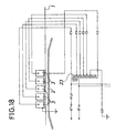
- a plurality of taps may be provided, for example, for the secondary winding of the transformer 23 of the high AC voltage power source AC as shown in FIG. 18 such that the voltages to be applied to the discharging elements 3 may exhibit a successive decrease in the travelling direction of the film 1.
- FIG. 19 shows a modified discharging station wherein a DC discharger of the positive and negative ion simultaneous production type is used for each of the discharging electrodes 3 of the discharging gate section 9 and a high positive DC voltage and a high negative DC voltage from the high DC voltage power source apparatus DC are applied at a time to the DC dischargers.
- each of the DC dischargers applies the high positive and negative DC voltages to those discharging needles arranged in a row in the widthwise direction of the film 1 such that they appear alternately in the direction of the arrangement of the discharging needles.
- a positive discharging needle and a negative discharging needle appear alternately in each row.
- the discharging needles may be divided alternately into rows of positive discharging needles and rows negative discharging needles to which high positive and negative DC voltages are applied separately from each other.
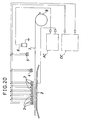
- FIG. 20 shows another modified discharging station wherein also the two DC dischargers 4 and 5 disposed between the discharging gate section 9 and the AC discharger 6 are formed from such DC dischargers of the positive and negative ion simultaneous production type as described above.
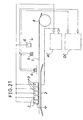
- FIG. 21 shows a further modified discharging station wherein the discharging electrodes 3 of the discharging gate section 9 are formed as discharging electrodes of the AC type while the two DC dischargers 4 and 5 are formed as DC dischargers of the positive and negative ion simultaneous production type.
- one of the two DC dischargers 4 and 5 can be omitted.
- FIG. 22 shows a still further modified discharging station wherein an ion attracting electrode 2 is opposed to each of a plurality of positive and negative ion producing discharging electrodes 3 arranged parallelly in the travelling direction of the film 1 so that positive and negative ions from each of the positive and negative ion producing discharging electrodes 3 are attracted to the corresponding ion attracting electrode 2.
- the high voltages to be applied to the parallel ion attracting electrode 2 are set so as to gradually decrease toward the travelling direction of the film 1.
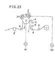
- FIG. 23 is a yet further modified discharging station wherein the ion attracting electrode 2 is formed from a roller for guiding the film 1 and the discharging electrodes 3 are disposed along an arc of the roller.
- the roller is formed from a metal cylindrical member and has a dielectric layer 60 formed on the surface thereof as seen in FIG. 24.
- Such a structure as shown in FIG. 23 achieves a higher discharging efficiency than that which is achieved where the ion attracting electrode 2 is spaced away from the film 1 as in the other examples described hereinabove. Further, also the size of the apparatus can be reduced.
- an AC discharging electrode or electrodes and a DC discharging electrode or electrodes may be disposed in an opposing relationship to the same ion attracting electrode 2.
Landscapes
- Elimination Of Static Electricity (AREA)
Description
Further, where the plastic film is a film to undergo printing, the surface of the film is treated by corona discharging in order to change the quality of the same to assure a high printing performance. As a result of such frictional charging and exfoliation discharging as well as corona discharging processing, an invisible charge pattern wherein a very large number of small positive and negative charged portions having very complicated shapes are formed closely to each other at random in a mixed condition is formed on each of the opposite front and back faces of the plastic film in accordance with manners of charging and manners of discharging. FIG. 8 illustrates an example of such invisible charge pattern which was made visible by scattering toner powder (black fine particles) of the negative polarity, which is normally used with a copying machine or the like, on a surface of a plastic film immediately after exfoliated from a roller so as to cause the toner powder to directly stick to the surface of the plastic film electrostatically and then transferring the sticking toner powder image, using a copying machine, to a paper sheet to obtain the figure shown in FIG. 8. Black portions to which toner powder stuck were positively charged portions while bright portions to which no toner powder stuck were negatively charged portions, and the intensity of the black color represents the magnitude of the electrostatic potential there.
Referring to FIGS. 5 and 6, the positive discharging
Claims (16)
- A discharging method wherein positive and negative ions are irradiated upon a travelling working object to discharge the working object, comprising the steps of:passing the working object (1) between a positive and negative ion producing discharging electrode apparatus (3) and an ion attracting electrode apparatus (2) disposed in an opposing relationship to said positive and negative ion producing discharging electrode apparatus (3) and having a face which extends in a travelling direction of the working object (1) and a widthwise direction;applying, while the working object (1) passes between said positive and negative ion producing discharging electrode apparatus (3) and said ion attracting electrode apparatus (2), high positive and negative voltages alternately to said positive and negative ion producing discharging electrode apparatus (3) to alternately produce positive and negative ions; andsimultaneously applying a high AC voltage to said ion attracting electrode apparatus (2) to induce positive and negative potentials in the working object so as to attract the positive and negative ions produced by said positive and negative ion producing discharging electrode apparatus (3) by the induced potentials of the working object (1),characterized in that a high AC voltage is applied to said positive and negative ion producing discharging electrode apparatus (3) to produce positive and negative ions while another high AC voltage having a higher frequency than that of the high AC voltage to said positive and negative ion producing discharging apparatus (3) is applied to said ion attracting apparatus (2).
- A discharging method as set forth in claim 1, characterized in that, said positive and negative ion producing discharging electrode apparatus (3) includes a positive ion producing electrode and a negative ion producing electrode, wherein a high positive voltage is applied to said positive ion producing electrode to produce positive ions and a high negative voltage is applied to said negative ion producing electrode to produce negative ions, and simultaneously a high AC voltage is applied to said ion attracting electrode apparatus (2).
- A discharging method as set forth in any preceding claim, characterized in that, said positive and negative ion producing discharging electrode apparatus (3) includes a plurality of positive and negative ion producing discharging electrodes (3) juxtaposed in the travelling direction of the working object (1) while said ion attracting electrode apparatus (2) includes a single attracting electrode (2) provided commonly to said positive and negative ion producing discharging electrodes (3), wherein high positive and negative voltages are applied to said positive and negative ion producing discharging electrodes (3) to produce positive and negative ions at a time while a high AC voltage is applied to said ion attracting electrode (2) to induce positive and negative potentials in the working object (1).
- A discharging method as set forth in any preceding claim, characterized in that, said positive and negative ion producing discharging electrode apparatus (3) includes a plurality of positive and negative ion producing discharging electrodes (3) juxtaposed in the travelling direction of the working object (1) while said ion attracting electrode apparatus (2) includes a plurality of ion attracting electrodes (2) individually corresponding to said positive and negative ion producing discharging electrodes (3), wherein high positive and negative voltages are applied to said positive and negative ion producing discharging electrodes (3) to produce positive and negative ions at a time while a high AC voltage is applied to said ion attracting electrodes (2) at a time to induce positive and negative potentials in the working object (1).
- A discharging method as set forth in claim 3, characterized in that different high voltages are applied to said positive and negative ion producing discharging electrodes (3) in such a manner as to successively decrease toward the travelling direction of the working object (1).
- A discharging method as set forth in claim 4, characterized in that different high voltages are applied to said ion attracting electrodes (2) in such a manner as to successively decrease toward the travelling direction of the working object (1).
- A discharging method as set forth in any preceding claim, characterized in that positive or negative ions produced by a DC discharger (4) are irradiated upon the working object (1), upon which positive and negative ions from said positive and negative ion producing discharging electrode apparatus (3) have been irradiated, in a weaker discharging condition than that by said positive and negative ion producing discharging electrode apparatus (3).
- A discharging method as set forth in claim 7, characterized in that, after positive or negative ions from said DC discharger (4) are irradiated upon the working object (1), positive and negative ions from an AC discharger are irradiated upon the working object (1) in a weaker discharging condition than that by said DC discharger (4).
- A discharging and dust removing method as set forth in any preceding claim, characterized in that air is jetted thereafter to the working object (1) while the working object (1) is travelling to remove dust or some other foreign articles from the working object (1).
- A discharging apparatus, comprising:an ion attracting electrode apparatus (2) having a face extending in a travelling direction of a travelling working object (1) and a widthwise direction;a positive and negative ion producing discharging electrode apparatus (3) opposed to said ion attracting apparatus (2) with a distance left therebetween sufficient to allow the working object (1) to pass therebetween; anda power source apparatus (AC) for applying high positive and negative voltages alternately to said positive and negative ion producing discharging electrode apparatus (3) to produce positive and negative ions alternately and simultaneously applying a high AC voltage to said ion attracting electrode apparatus (2) to induce positive and negative potentials in the working object so as to attract the positive and negative ions produced by said positive and negative ion producing discharging electrode apparatus (3) by the induced potentials of the working object (1),characterized in that said power source apparatus (AC) being adapted to apply a high AC voltage to said positive and negative ion producing discharging electrode apparatus (3) to produce positive and negative ions while to apply another high AC voltage having a higher frequency than that of the high AC voltage to said positive and negative ion producing discharging electrode apparatus (3) to said ion attracting electrode apparatus (2).
- A discharging apparatus as set forth in claim 10, characterized in that said positive and negative ion producing discharging electrode apparatus (3) includes a plurality of positive and negative ion producing discharging electrodes (3) juxtaposed in the travelling direction of the working object (1), and said ion attracting electrode apparatus (2) includes a single ion attracting electrode (2) in the form of a plate disposed in an opposing relationship commonly to said positive and negative ion producing discharging electrodes (3).
- A discharging apparatus as set forth in claim 11, characterized in that said ion discharging electrode (2) is inclined in such a manner that a distance thereof to said positive and negative ion producing discharging electrode apparatus (3) successively increases toward the travelling direction of the working object (1).
- A discharging apparatus as set forth in any of the claims 10 to 12, characterized in that said positive and negative ion producing discharging electrode apparatus (3) includes a roller which rotates to guide the travelling working object (1).
- A discharging apparatus as set forth in claim 13, characterized in that said ion attracting electrode apparatus (2) includes a metal roller (2) having a dielectric layer (60) formed on a surface thereof.
- A discharging apparatus as set forth in any of claims 10 to 14, characterized in that it further comprises a mechanism for varying a distance between said positive and negative ion producing discharging electrode apparatus (3) and said ion attracting electrode apparatus (2).
- A discharging apparatus as set forth in any of claims 10 to 15, characterized byan air shower dust removing unit (50) including an air jetting section (50a) for jetting air to the working object (1) which has been discharged by said positive and negative ion producing discharging electrode apparatus (3) and said ion attracting electrode apparatus (2) and an air sucking section (50b, 50c) for sucking the air jetted from said air jetting section (50a).
Priority Applications (3)
| Application Number | Priority Date | Filing Date | Title |
|---|---|---|---|
| EP19950115076 EP0766501B1 (en) | 1995-09-25 | 1995-09-25 | Discharging and dust removing method and apparatus |
| DE1995606251 DE69506251T2 (en) | 1995-09-25 | 1995-09-25 | Method and device for charge removal and dedusting |
| DK95115076T DK0766501T3 (en) | 1995-09-25 | 1995-09-25 | Process for discharging and removing dust and apparatus for carrying out the process |
Applications Claiming Priority (1)
| Application Number | Priority Date | Filing Date | Title |
|---|---|---|---|
| EP19950115076 EP0766501B1 (en) | 1995-09-25 | 1995-09-25 | Discharging and dust removing method and apparatus |
Publications (2)
| Publication Number | Publication Date |
|---|---|
| EP0766501A1 EP0766501A1 (en) | 1997-04-02 |
| EP0766501B1 true EP0766501B1 (en) | 1998-11-25 |
Family
ID=8219650
Family Applications (1)
| Application Number | Title | Priority Date | Filing Date |
|---|---|---|---|
| EP19950115076 Expired - Lifetime EP0766501B1 (en) | 1995-09-25 | 1995-09-25 | Discharging and dust removing method and apparatus |
Country Status (3)
| Country | Link |
|---|---|
| EP (1) | EP0766501B1 (en) |
| DE (1) | DE69506251T2 (en) |
| DK (1) | DK0766501T3 (en) |
Cited By (2)
| Publication number | Priority date | Publication date | Assignee | Title |
|---|---|---|---|---|
| DE10018010A1 (en) * | 2000-04-11 | 2001-10-25 | Eltex Elektrostatik Gmbh | Dust extraction device has corona charging electrode and counter electrode on either side of material, discharge electrode and suction device close to discharge electrode, preferably after it |
| DE102005061332A1 (en) * | 2005-12-21 | 2007-06-28 | Eltex-Elektrostatik Gmbh | Device for contactless removal of electrostatic electrical double layer from flat electrically insulating material has contactless compensating device for feed of charge particles to flat material for compensation of charges |
Families Citing this family (4)
| Publication number | Priority date | Publication date | Assignee | Title |
|---|---|---|---|---|
| DE10023939A1 (en) * | 2000-05-17 | 2001-11-22 | Heidelberger Druckmasch Ag | Device for removing electrical charges from flat material |
| JP5435423B2 (en) * | 2009-12-09 | 2014-03-05 | Smc株式会社 | Ionizer and static elimination method |
| CN103128828A (en) * | 2011-12-03 | 2013-06-05 | 苏州豪特景精密机械有限公司 | Floor production device |
| CN111001639B (en) * | 2019-12-10 | 2020-11-10 | 昆山聚创新能源科技有限公司 | Method for preventing dust cross contamination of anode and cathode in baking process |
Family Cites Families (7)
| Publication number | Priority date | Publication date | Assignee | Title |
|---|---|---|---|---|
| US2483542A (en) * | 1945-10-24 | 1949-10-04 | Goss Printing Press Co Ltd | Static eliminator for printing presses |
| US3474292A (en) * | 1966-03-01 | 1969-10-21 | Du Pont | Method of reducing electrostatic charges on film structures |
| US3475652A (en) * | 1966-12-05 | 1969-10-28 | Simco Co Inc The | Dual phase static eliminator |
| GB1181368A (en) * | 1967-08-16 | 1970-02-18 | Agfa Gevaert Nv | Electrostatic cleaner |
| DE2639706A1 (en) * | 1975-10-06 | 1977-04-14 | Ibm | Neutralisation of static charge on electrophotographic ribbon |
| US4750080A (en) * | 1987-02-13 | 1988-06-07 | Cumming Corporation | Film cleaner method and apparatus |
| JPS63301495A (en) * | 1987-06-02 | 1988-12-08 | Kasuga Denki Kk | How to remove static electricity from a charged moving object |
-
1995
- 1995-09-25 EP EP19950115076 patent/EP0766501B1/en not_active Expired - Lifetime
- 1995-09-25 DE DE1995606251 patent/DE69506251T2/en not_active Expired - Lifetime
- 1995-09-25 DK DK95115076T patent/DK0766501T3/en active
Cited By (4)
| Publication number | Priority date | Publication date | Assignee | Title |
|---|---|---|---|---|
| DE10018010A1 (en) * | 2000-04-11 | 2001-10-25 | Eltex Elektrostatik Gmbh | Dust extraction device has corona charging electrode and counter electrode on either side of material, discharge electrode and suction device close to discharge electrode, preferably after it |
| DE10018010C2 (en) * | 2000-04-11 | 2003-10-16 | Eltex Elektrostatik Gmbh | Dust removal device and its use |
| DE102005061332A1 (en) * | 2005-12-21 | 2007-06-28 | Eltex-Elektrostatik Gmbh | Device for contactless removal of electrostatic electrical double layer from flat electrically insulating material has contactless compensating device for feed of charge particles to flat material for compensation of charges |
| DE102005061332B4 (en) * | 2005-12-21 | 2017-11-23 | Eltex-Elektrostatik Gmbh | Device for contactless elimination of an electrostatic charge double layer |
Also Published As
| Publication number | Publication date |
|---|---|
| DE69506251D1 (en) | 1999-01-07 |
| DK0766501T3 (en) | 1999-08-09 |
| DE69506251T2 (en) | 1999-04-22 |
| EP0766501A1 (en) | 1997-04-02 |
Similar Documents
| Publication | Publication Date | Title |
|---|---|---|
| US5683556A (en) | Discharging and dust removing method and discharging and dust removing apparatus | |
| US4491855A (en) | Image recording method and apparatus | |
| US4478510A (en) | Cleaning device for modulation control means | |
| US3396308A (en) | Web treating device | |
| US4901666A (en) | Electrostatic powder coating device | |
| US3536528A (en) | Electrostatic cleaner and method | |
| US6597884B2 (en) | Image forming apparatus including electrostatic conveyance of charged toner | |
| GB2108432A (en) | Electrographic printing | |
| DE69006949T2 (en) | Electrostatic pressure device. | |
| US5400208A (en) | Web edge discharging system | |
| EP0111400A2 (en) | Apparatus for controlling random charges on a moving web | |
| EP0766501A1 (en) | Discharging and dust removing method and apparatus | |
| JP3069837B2 (en) | How to check static elimination of film etc. | |
| JPH01139277A (en) | Ion printer having ion focussing means | |
| US4664502A (en) | Liquid developing apparatus for use in electrophotographic copying machine | |
| JP2002289394A (en) | Insulating sheet static elimination method and apparatus | |
| KR0181552B1 (en) | Antistatic and vibration suppression method and antistatic and vibration suppression device | |
| JP4396084B2 (en) | Manufacturing method of electrical insulating sheet | |
| JP2651476B2 (en) | Method and device for removing static electricity from films | |
| JP3517968B2 (en) | Insulating web static elimination method and web manufacturing method | |
| US4827295A (en) | Conditioning apparatus for non-impact, direct charge electrographic printer belt | |
| JP3455984B2 (en) | Static electricity removal method for charged traveling body | |
| JP4871036B2 (en) | Static elimination method and static elimination device | |
| JPS58104769A (en) | Recorder for picture | |
| ATE272261T1 (en) | DEVICE FOR ELECTRICALLY CHARGING A WEB-SHAPED SUBSTRATE |
Legal Events
| Date | Code | Title | Description |
|---|---|---|---|
| PUAI | Public reference made under article 153(3) epc to a published international application that has entered the european phase |
Free format text: ORIGINAL CODE: 0009012 |
|
| 17P | Request for examination filed |
Effective date: 19960926 |
|
| AK | Designated contracting states |
Kind code of ref document: A1 Designated state(s): CH DE DK GB IT LI SE |
|
| 17Q | First examination report despatched |
Effective date: 19970506 |
|
| GRAG | Despatch of communication of intention to grant |
Free format text: ORIGINAL CODE: EPIDOS AGRA |
|
| GRAG | Despatch of communication of intention to grant |
Free format text: ORIGINAL CODE: EPIDOS AGRA |
|
| GRAH | Despatch of communication of intention to grant a patent |
Free format text: ORIGINAL CODE: EPIDOS IGRA |
|
| GRAH | Despatch of communication of intention to grant a patent |
Free format text: ORIGINAL CODE: EPIDOS IGRA |
|
| GRAH | Despatch of communication of intention to grant a patent |
Free format text: ORIGINAL CODE: EPIDOS IGRA |
|
| GRAA | (expected) grant |
Free format text: ORIGINAL CODE: 0009210 |
|
| AK | Designated contracting states |
Kind code of ref document: B1 Designated state(s): CH DE DK GB IT LI SE |
|
| REG | Reference to a national code |
Ref country code: CH Ref legal event code: NV Representative=s name: PA ALDO ROEMPLER Ref country code: CH Ref legal event code: EP |
|
| REF | Corresponds to: |
Ref document number: 69506251 Country of ref document: DE Date of ref document: 19990107 |
|
| ITF | It: translation for a ep patent filed | ||
| REG | Reference to a national code |
Ref country code: DK Ref legal event code: T3 |
|
| PLBE | No opposition filed within time limit |
Free format text: ORIGINAL CODE: 0009261 |
|
| STAA | Information on the status of an ep patent application or granted ep patent |
Free format text: STATUS: NO OPPOSITION FILED WITHIN TIME LIMIT |
|
| 26N | No opposition filed | ||
| REG | Reference to a national code |
Ref country code: GB Ref legal event code: IF02 |
|
| REG | Reference to a national code |
Ref country code: CH Ref legal event code: PCAR Free format text: ALDO ROEMPLER PATENTANWALT;BRENDENWEG 11 POSTFACH 154;9424 RHEINECK (CH) |
|
| PGFP | Annual fee paid to national office [announced via postgrant information from national office to epo] |
Ref country code: DE Payment date: 20140922 Year of fee payment: 20 Ref country code: DK Payment date: 20140924 Year of fee payment: 20 Ref country code: CH Payment date: 20140922 Year of fee payment: 20 |
|
| PGFP | Annual fee paid to national office [announced via postgrant information from national office to epo] |
Ref country code: GB Payment date: 20140923 Year of fee payment: 20 Ref country code: SE Payment date: 20140923 Year of fee payment: 20 |
|
| PGFP | Annual fee paid to national office [announced via postgrant information from national office to epo] |
Ref country code: IT Payment date: 20140923 Year of fee payment: 20 |
|
| REG | Reference to a national code |
Ref country code: DE Ref legal event code: R071 Ref document number: 69506251 Country of ref document: DE |
|
| REG | Reference to a national code |
Ref country code: DK Ref legal event code: EUP Effective date: 20150925 |
|
| REG | Reference to a national code |
Ref country code: CH Ref legal event code: PL |
|
| REG | Reference to a national code |
Ref country code: GB Ref legal event code: PE20 Expiry date: 20150924 |
|
| PG25 | Lapsed in a contracting state [announced via postgrant information from national office to epo] |
Ref country code: GB Free format text: LAPSE BECAUSE OF EXPIRATION OF PROTECTION Effective date: 20150924 |
|
| REG | Reference to a national code |
Ref country code: SE Ref legal event code: EUG |