EP0765008B1 - Stacked electrical connector assembly - Google Patents
Stacked electrical connector assembly Download PDFInfo
- Publication number
- EP0765008B1 EP0765008B1 EP96306869A EP96306869A EP0765008B1 EP 0765008 B1 EP0765008 B1 EP 0765008B1 EP 96306869 A EP96306869 A EP 96306869A EP 96306869 A EP96306869 A EP 96306869A EP 0765008 B1 EP0765008 B1 EP 0765008B1
- Authority
- EP
- European Patent Office
- Prior art keywords
- contact
- connector assembly
- segments
- electrical connector
- retention member
- Prior art date
- Legal status (The legal status is an assumption and is not a legal conclusion. Google has not performed a legal analysis and makes no representation as to the accuracy of the status listed.)
- Expired - Lifetime
Links
- 230000014759 maintenance of location Effects 0.000 claims description 23
- 230000000712 assembly Effects 0.000 description 9
- 238000000429 assembly Methods 0.000 description 9
- 238000003780 insertion Methods 0.000 description 6
- 230000037431 insertion Effects 0.000 description 6
- 238000005452 bending Methods 0.000 description 5
- 239000000654 additive Substances 0.000 description 1
- 230000000996 additive effect Effects 0.000 description 1
- 238000006073 displacement reaction Methods 0.000 description 1
- 239000000463 material Substances 0.000 description 1
- 230000013011 mating Effects 0.000 description 1
- 239000002184 metal Substances 0.000 description 1
Images

Classifications
-
- H—ELECTRICITY
- H01—ELECTRIC ELEMENTS
- H01R—ELECTRICALLY-CONDUCTIVE CONNECTIONS; STRUCTURAL ASSOCIATIONS OF A PLURALITY OF MUTUALLY-INSULATED ELECTRICAL CONNECTING ELEMENTS; COUPLING DEVICES; CURRENT COLLECTORS
- H01R12/00—Structural associations of a plurality of mutually-insulated electrical connecting elements, specially adapted for printed circuits, e.g. printed circuit boards [PCB], flat or ribbon cables, or like generally planar structures, e.g. terminal strips, terminal blocks; Coupling devices specially adapted for printed circuits, flat or ribbon cables, or like generally planar structures; Terminals specially adapted for contact with, or insertion into, printed circuits, flat or ribbon cables, or like generally planar structures
- H01R12/70—Coupling devices
- H01R12/71—Coupling devices for rigid printing circuits or like structures
- H01R12/712—Coupling devices for rigid printing circuits or like structures co-operating with the surface of the printed circuit or with a coupling device exclusively provided on the surface of the printed circuit
- H01R12/716—Coupling device provided on the PCB
-
- H—ELECTRICITY
- H01—ELECTRIC ELEMENTS
- H01R—ELECTRICALLY-CONDUCTIVE CONNECTIONS; STRUCTURAL ASSOCIATIONS OF A PLURALITY OF MUTUALLY-INSULATED ELECTRICAL CONNECTING ELEMENTS; COUPLING DEVICES; CURRENT COLLECTORS
- H01R25/00—Coupling parts adapted for simultaneous co-operation with two or more identical counterparts, e.g. for distributing energy to two or more circuits
- H01R25/006—Coupling parts adapted for simultaneous co-operation with two or more identical counterparts, e.g. for distributing energy to two or more circuits the coupling part being secured to apparatus or structure, e.g. duplex wall receptacle
Definitions
- This invention relates generally to so-called stacked electrical connector assemblies and pertains more particularly to stacked electrical connector assemblies of type having contact tails for insertion into printed circuit boards or other mating structure adapted for receipt of contact tails depending from one or more of the discrete stacked connectors of the assemblies.
- a known version of a stacked connector assembly is seen in the HANDBOOK OF D-SUBMINIATURE CONNECTORS MIL-C 24308 & MIL-C39029 , of Positronic Industries, Inc.
- the assembly has an upper connector and a lower connector, having respective right-angle contact elements extending rearwardly and downwardly of the assembly for insertion into a printed circuit board (PCB).
- PCB printed circuit board
- Both connector bodies are secured to side brackets and a "locking support member" serves to enhance positioning of the contact elements as the contact elements exit the assembly and enter counterpart holes in the PCB.
- Other known stacked connector assemblies are shown in various U.S. patents, for example, No. 4,612,602, No. 4,818,239, No. 4,878,856, No. 5,044,984 and No. 5,336,109.
- a difficulty with various of the above-referenced known stacked connector assemblies resides in the exposure of contact element tails to bending and other deformation in the course of their insertion into the PCB, and potential failure to properly seat in the PCB holes despite the presence of the locking support members.
- the locking support members thereof impose only lateral positional retention constraints on the contact tails.
- pin extension member 16 which serves to electrically extend the contact elements 32 of the upper connector body.
- the contact pins of the pin extension member are encased in rigid plastic, virtually precluding deformation thereof.
- Such solution increases both the cost of the stacked connector assembly in respect of pin contact extensions and encasing plastic. Assembly thereof is also complicated to the extent of requiring steps of inserting the shortened contacts of the upper connector element into the pin extension members. Further, connector electrical performance has concern in respect of the additional connection interface required as between the shortened contacts of the upper connector and the pin extension members.
- US-A-4842528 discloses an electrical connector assembly having an upper row of contact elements, each having a first segment extending rearwardly therein and a second segment extending downwardly from the first segment, a lower row of contacts each having a first segment extending rearwardly therein and a second segment extending downwardly from the first segment, support means for supporting the contact elements in the assembly, and a contact retention member having a plurality of contact receiving slots for receiving the second segments of the contact elements, the second segment of each contact element having spaced apart stop means for engaging either side of the contact retention member to retain the contact second segments against vertical movement relative to the contact retention member.
- US-A-4842528 requires insertion of contact second segments transversely into the contact receiving slots, as opposed to insertion in the axial direction of the contact element second segments.
- the present invention has as its primary object the provision of stacked electrical connector assemblies having enhanced resistance to contact tail bending or deformation.
- a more particular object of the invention is to provide stacked electrical connector assemblies which achieve multi-directional contact tail retention without need for structure encasing the contact tails over extended lengths thereof.
- the invention provides a stacked electrical connector assembly, comprising:
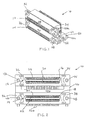
- Fig. 1 is a perspective view of a stacked electrical connector assembly in accordance with the invention.
- Fig. 2 is a front elevation of the Fig. 1 assembly.
- Fig. 3 is a right side elevation of Fig. 2.
- Fig. 4 is a right side elevation of Fig. 3, constituting a rear elevation of Fig. 2.
- Fig. 5 is a partial sectional view as would be seen from plane V-V of Fig. 3.
- stacked electrical connector assembly 10 includes upper connector 12, lower connector 14, having respective housings 16 and 18 of electrically insulative material.
- Female to male contact elements 20 and 22 are resident respectively in housings 16 and 18 in respective upper and lower rows.
- Contacts 20 have right-angle tail portions 24a and 24b continuous with contacts 20 in the upper row and right-angle tail portions 24c and 24d continuous with contacts 20 in the lower row.
- Contacts 22 have right-angle tail portions 26a and 26b continuous with contacts 22 in the upper row and right-angle tail portions 26c and 26d continuous with contacts 22 in the lower row.
- Bracket 40 further includes rearwardly extending, transversely spaced side members 40b and 40c.
- contact retention structure 50 in accordance with the invention has a central portion defining passages 50a for contact tails to pass therethrough and outer portions 50b and 50c.
- Structure 50 is disposed atop transversely spaced side members 40b and 40c and is secured thereto by rivets, one being shown at 52 in Fig. 1, extending through apertures in outer portions 50b and 50c.
- Structure 50 is comprised of an electrically insulative member and defines interior deflectable portions 50d, each in respective partial bounding relation to a distinct one of passages 50a.
- the insulative member of the contact retention means is elongate and supports the deflectable parts for deflection along the longitudinal axis thereof.
- contact 24a-1 resident in passage 50a-1, it has a tail portion of generally rectangular cross-section in the passage of the insulative member and has a detent defined by a radially interiorly extending notch in the cross-section portion.
- contact cross-sections of other configurations such as cylindrical or U-shape, could also be used.
- the insulative member has respective upper and lower mutually parallel planar surfaces 50e and 50f, between which passage 50a-1 extends and deflectable part 50d-1 is cantilever-supported and disposed at an angle intersecting the planes of upper and lower surfaces 50e and 50f.
- the contact 24a-1 detent notch is defined by a floor 24a-1a generally parallel to upper and lower surfaces 50e and 50f of the insulative member and a wall 24a-1b extending from floor 24a-1a at substantially the same angle as the disposition angle of the cantilever-supported part 50d-1 of the insulative member.
- the insulative member has continuous, undeflectable surface in bounding relation to passage 50a-1.
Landscapes
- Coupling Device And Connection With Printed Circuit (AREA)
- Connector Housings Or Holding Contact Members (AREA)
- Multi-Conductor Connections (AREA)
Description
- This invention relates generally to so-called stacked electrical connector assemblies and pertains more particularly to stacked electrical connector assemblies of type having contact tails for insertion into printed circuit boards or other mating structure adapted for receipt of contact tails depending from one or more of the discrete stacked connectors of the assemblies.
- A known version of a stacked connector assembly, commercially available for at least a decade, is seen in the HANDBOOK OF D-SUBMINIATURE CONNECTORS MIL-C 24308 & MIL-C39029, of Positronic Industries, Inc. The assembly has an upper connector and a lower connector, having respective right-angle contact elements extending rearwardly and downwardly of the assembly for insertion into a printed circuit board (PCB). Both connector bodies are secured to side brackets and a "locking support member" serves to enhance positioning of the contact elements as the contact elements exit the assembly and enter counterpart holes in the PCB. Other known stacked connector assemblies are shown in various U.S. patents, for example, No. 4,612,602, No. 4,818,239, No. 4,878,856, No. 5,044,984 and No. 5,336,109.
- Where the downward extents of contact elements of the upper connector of a stacked connector assembly are of short length, or where the contacts are relatively thick and thus self-sustaining in right angle disposition, the prior art may look to direct insertion of the end tails of such contacts in a PCB, as is seemingly shown in Fig. 12 of the '602 patent. On the other hand, where the downward extents of contact elements of the upper connector of a stacked connector assembly are of long length and/or where the contacts are relatively thin and thus not self-sustaining in right angle disposition, the prior art has looked to the locking support member, noted above for the long-standing commercial Positronic stacked connector assembly. Various such locking support members are evidenced in the above-noted patents other than the '602 patent.
- A difficulty with various of the above-referenced known stacked connector assemblies, from applicant's viewpoint, resides in the exposure of contact element tails to bending and other deformation in the course of their insertion into the PCB, and potential failure to properly seat in the PCB holes despite the presence of the locking support members. Thus, with the exception of the additive structure shown in the connector assemblies of the '239 and '856 patents, there is no structure at hand which confines the right-angle portions of the contact elements from such bending or other deformation. The locking support members thereof impose only lateral positional retention constraints on the contact tails.
- While the prior art approach adopted in the '239 and '856 patents has less susceptibility to such bending and other deformation, it is achieved only at the cost of so-called "
pin extension member 16", which serves to electrically extend thecontact elements 32 of the upper connector body. The contact pins of the pin extension member are encased in rigid plastic, virtually precluding deformation thereof. Evidently, such solution increases both the cost of the stacked connector assembly in respect of pin contact extensions and encasing plastic. Assembly thereof is also complicated to the extent of requiring steps of inserting the shortened contacts of the upper connector element into the pin extension members. Further, connector electrical performance has concern in respect of the additional connection interface required as between the shortened contacts of the upper connector and the pin extension members. - US-A-4842528 discloses an electrical connector assembly having an upper row of contact elements, each having a first segment extending rearwardly therein and a second segment extending downwardly from the first segment, a lower row of contacts each having a first segment extending rearwardly therein and a second segment extending downwardly from the first segment, support means for supporting the contact elements in the assembly, and a contact retention member having a plurality of contact receiving slots for receiving the second segments of the contact elements, the second segment of each contact element having spaced apart stop means for engaging either side of the contact retention member to retain the contact second segments against vertical movement relative to the contact retention member.
- US-A-4842528 requires insertion of contact second segments transversely into the contact receiving slots, as opposed to insertion in the axial direction of the contact element second segments.
- The present invention has as its primary object the provision of stacked electrical connector assemblies having enhanced resistance to contact tail bending or deformation.
- A more particular object of the invention is to provide stacked electrical connector assemblies which achieve multi-directional contact tail retention without need for structure encasing the contact tails over extended lengths thereof.
- The invention provides a stacked electrical connector assembly, comprising:
- (a) an upper connector having a plurality of contact elements, each having a first segment rearwardly therein and a second segment extending downwardly from said first segment;
- (b) a lower connector having a plurality of contact elements, each having a first segment extending rearwardly therein and a second segment extending downwardly from said first segment; and
- (c) support means for supporting said upper and lower connectors in vertically spaced relation and having transversely spaced elements extending rewardly from and vertically below said lower connector; the support means further including a contact retention member disposed between said transversely spaced elements of said support means, the contact retention member having a plurality of contact receiving passages for receiving at least said second segments of said contacts of each of said upper and lower connectors and wherein each of the contact receiving passages includes a cantilevered deflectable portion for locking engagement with said second segments of said contacts thereby aligning and retaining the received contact second segments against both transverse and vertically upward movements relative to said connector assembly.
-
- The foregoing and other objects and features of the invention will be further understood from the following detailed discussion of preferred practices and embodiments thereof and from the drawings wherein like reference numerals identify like components and part throughout.
- Fig. 1 is a perspective view of a stacked electrical connector assembly in accordance with the invention.
- Fig. 2 is a front elevation of the Fig. 1 assembly.
- Fig. 3 is a right side elevation of Fig. 2.
- Fig. 4 is a right side elevation of Fig. 3, constituting a rear elevation of Fig. 2.
- Fig. 5 is a partial sectional view as would be seen from plane V-V of Fig. 3.
- Referring to Figs. 1-4, stacked
electrical connector assembly 10 includesupper connector 12,lower connector 14, havingrespective housings male contact elements 20 and 22 are resident respectively inhousings Contacts 20 have right-angle tail portions 24a and 24b continuous withcontacts 20 in the upper row and right-angle tail portions 24c and 24d continuous withcontacts 20 in the lower row. Contacts 22 have right-angle tail portions 26a and 26b continuous with contacts 22 in the upper row and right-angle tail portions 26c and 26d continuous with contacts 22 in the lower row. -
Metal shell members connectors end blocks bracket 40 is secured, through avertical section 40a thereof toupper connector 12, byrivets vertical section 40a tolower connector 14, byrivets Bracket 40 further includes rearwardly extending, transversely spaced side members 40b and 40c. - Referring now also to Fig. 5,
contact retention structure 50 in accordance with the invention has a centralportion defining passages 50a for contact tails to pass therethrough and outer portions 50b and 50c.Structure 50 is disposed atop transversely spaced side members 40b and 40c and is secured thereto by rivets, one being shown at 52 in Fig. 1, extending through apertures in outer portions 50b and 50c. -
Structure 50 is comprised of an electrically insulative member and defines interiordeflectable portions 50d, each in respective partial bounding relation to a distinct one ofpassages 50a. The insulative member of the contact retention means is elongate and supports the deflectable parts for deflection along the longitudinal axis thereof. - As illustrated for
contact 24a-1, resident inpassage 50a-1, it has a tail portion of generally rectangular cross-section in the passage of the insulative member and has a detent defined by a radially interiorly extending notch in the cross-section portion. It should be appreciated that contact cross-sections of other configurations, such as cylindrical or U-shape, could also be used. More particularly, the insulative member has respective upper and lower mutually parallelplanar surfaces 50e and 50f, between whichpassage 50a-1 extends anddeflectable part 50d-1 is cantilever-supported and disposed at an angle intersecting the planes of upper andlower surfaces 50e and 50f. Thecontact 24a-1 detent notch is defined by afloor 24a-1a generally parallel to upper andlower surfaces 50e and 50f of the insulative member and awall 24a-1b extending fromfloor 24a-1a at substantially the same angle as the disposition angle of the cantilever-supportedpart 50d-1 of the insulative member. - Other than for the
deflectable part 50d-1, the insulative member has continuous, undeflectable surface in bounding relation topassage 50a-1. - The described cantilever-supported part and the remnant continuous bounding surface of the passages in
contact retention structure 50 will be appreciated as achieving the contact tail positioning function of the prior art connector assemblies having contact "locking support structure", above discussed. Significantly, however,structure 50, based on its inclusion of the coaction of the deflectable part further with the contact tail detents, provides the further function of providing resistance to upward displacement of the contacts received in the contact retention structure passages. Thus, as the assembled connector is applied to a PCB, at which time snap latches 40b-1 and 40c-1 depending from side members 40b and 40c secure the assembly to the PCB, upward force exerted by the PCB on the contact tails is arrested and absorbed at the detent-deflectable part interface, and is precluded from imparting bending or other deformation to the right-angle segments of the contacts.
Claims (11)
- The invention provides a stacked electrical connector assembly (10), comprising:(a) an upper connector (12) having a plurality of contact elements (20), each having a first segment rearwardly therein and a second segment (24) extending downwardly from said first segment;(b) a lower connector (14) having a plurality of contact elements (22), each having a first segment extending rearwardly therein and a second segment (26) extending downwardly from said first segment; and(c) support means (40) for supporting said upper and lower connectors (12, 14) in vertically spaced relation and having transversely spaced elements (40b, 40c) extending rewardly from and vertically below said lower connector (14); the support means further including a contact retention member (50) disposed between said transversely spaced elements (40b, 40c) of said support means (40), the contact retention member (50) having a plurality of contact receiving passages (50a) for receiving at least said second segments (24, 26) of said contacts of each of said upper and lower connectors and wherein each of the contact receiving passages (50a) includes a cantilevered deflectable portion (50d) for locking engagement with said second segments (24, 26) of said contacts thereby aligning and retaining the received contact second segments against both transverse and vertically upward movements relative to said connector assembly (10).
- The stacked electrical connector assembly claimed in claim 1, wherein said contact retention member comprises an electrically insulative member (50).
- The stacked electrical connector assembly claimed in claim 1, or claim 2, wherein said contact retention member (50) is disposed vertically above said transversely spaced elements (40b, 40c) of said support means (40) and is secured thereto.
- The stacked connector assembly claimed in any one of claims 1 to 3, wherein some of said plurality of contact second segments (26) of said lower connector (14) are located in respective first planes successively rearwardly disposed in said assembly and wherein some of said plurality of contact second segments (24) of said upper connector (12) are located in respective second planes successively rearwardly disposed in said assembly, said second planes being rearwardly successive to said first planes.
- The stacked electrical connector assembly claimed in any one of claims 1 to 4, wherein the received contact second segments (24, 26) define respective detents and wherein the deflectable portions of said contact retention plate are lockingly engaged in said detents.
- The stacked electrical connector assembly claimed in claim 5, wherein said contact retention member (50) is elongate and supports said deflectable portions (50d) for deflection along a longitudinal axis thereof.
- The stacked electrical connector assembly claimed in claim 6, wherein the received contact second segments (24, 26) have portions of generally rectangular cross-section in said passages of said insulative member and wherein said detents of the received contact second segments are defined by radially interiorly extending notches in said cross-section portions.
- The stacked electrical connector assembly claimed in claim 6, wherein said contact retention member (50) has respective upper and lower mutually parallel planar surfaces (50e, 50f) wherein said passages (50a) extend between said upper and lower surfaces (50e, 50f) and wherein said deflectable portions (50d) of said contact retention member are disposed at an angle intersecting the mutually parallel planar surfaces (50e, 50f) of said contact retention member.
- The stacked electrical connector assembly claimed in claim 8, wherein the received contact second segments (24, 26) have portions of generally rectangular cross-section in said passages (50a) of said contact retention member and wherein said detents of the received contact second segments (24, 26) are defined by a floor (24-1a) generally parallel to said upper and lower surfaces of said contact retention member and a wall (24-1b) extending from said floor at substantially the same angle as the disposition angle of said cantilever-supported deflectable portions (50d) of said contact retention member (50).
- The stacked electrical connector assembly claimed in any one of claims 1 to 9, wherein said support means includes securement elements for securing said connector assembly (10) to a printed circuit board.
- The stacked electrical connector assembly claimed in claim 10, wherein said securement elements are in downwardly depending relation from said transversely spaced elements (40b, 40c) of said support means (40).
Applications Claiming Priority (2)
| Application Number | Priority Date | Filing Date | Title |
|---|---|---|---|
| US530800 | 1995-09-20 | ||
| US08/530,800 US5733143A (en) | 1995-09-20 | 1995-09-20 | Stacked electrical connector assembly |
Publications (2)
| Publication Number | Publication Date |
|---|---|
| EP0765008A1 EP0765008A1 (en) | 1997-03-26 |
| EP0765008B1 true EP0765008B1 (en) | 2002-01-23 |
Family
ID=24115033
Family Applications (1)
| Application Number | Title | Priority Date | Filing Date |
|---|---|---|---|
| EP96306869A Expired - Lifetime EP0765008B1 (en) | 1995-09-20 | 1996-09-20 | Stacked electrical connector assembly |
Country Status (6)
| Country | Link |
|---|---|
| US (1) | US5733143A (en) |
| EP (1) | EP0765008B1 (en) |
| JP (1) | JP3024069B2 (en) |
| CA (1) | CA2185974A1 (en) |
| DE (1) | DE69618728T2 (en) |
| SG (1) | SG85083A1 (en) |
Families Citing this family (18)
| Publication number | Priority date | Publication date | Assignee | Title |
|---|---|---|---|---|
| JP3104616B2 (en) * | 1996-04-25 | 2000-10-30 | 住友電装株式会社 | Board connector |
| TW330737U (en) * | 1997-06-05 | 1998-04-21 | Hon Hai Prec Ind Co Ltd | Connector for high density plugs |
| USD414465S (en) | 1997-08-27 | 1999-09-28 | Hon Hai Precision Ind. Co., Ltd. | Electrical connector |
| USD411174S (en) | 1998-05-06 | 1999-06-22 | Hon Hai Precision Ind. Co., Ltd. | Multi-post electrical connector |
| USD414161S (en) | 1998-05-27 | 1999-09-21 | Hon Hai Precision Ind. Co., Ltd. | Stacked electrical connector assembly |
| USD414162S (en) | 1998-06-16 | 1999-09-21 | Hon Hai Precision Ind. Co., Ltd. | Electrical connector assembly |
| USD414467S (en) | 1998-10-21 | 1999-09-28 | Honda Tsushin Kogyo Co., Ltd. | Double jack male type connector |
| JP2001006771A (en) * | 1999-06-18 | 2001-01-12 | Nec Corp | Connector |
| US6146194A (en) * | 1999-08-17 | 2000-11-14 | Hon Hai Precision Ind. Co., Ltd. | Stacked connector assembly |
| US6302731B1 (en) * | 1999-09-16 | 2001-10-16 | Kycon, Incorporated | Bracket for connector |
| USD433384S (en) * | 2000-05-09 | 2000-11-07 | Hon Hai Precision Ind. Co., Ltd. | Stacked connector |
| JP2003031324A (en) | 2001-07-18 | 2003-01-31 | Jst Mfg Co Ltd | Electrical connector assembly |
| USD470112S1 (en) | 2001-09-14 | 2003-02-11 | Honda Tsushin Kogyo Co., Ltd. | Interface connector receptacle |
| USD467549S1 (en) | 2001-12-28 | 2002-12-24 | Hon Hai Precision Ind. Co., Ltd. | Electrical connector |
| US6688908B2 (en) | 2002-01-11 | 2004-02-10 | Kycon, Incorporated | Stacked DC power jack with LED |
| US8864518B2 (en) * | 2013-01-20 | 2014-10-21 | International Business Machines Corporation | Stack connector component having high speed and low speed pins |
| USD1114741S1 (en) * | 2020-03-17 | 2026-02-24 | Yamaichi Electronics Co., Ltd. | Connector for an optical module |
| CN112993624B (en) * | 2021-02-05 | 2022-09-06 | 深圳市豪塑科技有限公司 | Double-position connector and assembling method thereof |
Family Cites Families (8)
| Publication number | Priority date | Publication date | Assignee | Title |
|---|---|---|---|---|
| US3066272A (en) * | 1958-10-01 | 1962-11-27 | Whitney Blake Co | Axially mating electrical connector |
| US3255427A (en) * | 1964-03-03 | 1966-06-07 | Amp Inc | Multi-contact connector |
| US3747047A (en) * | 1971-12-01 | 1973-07-17 | Hughes Aircraft Co | Latchable integrally molded electrical connector |
| US4023880A (en) * | 1974-08-09 | 1977-05-17 | International Telephone And Telegraph Corporation | Contact retention assembly |
| DE3330151A1 (en) * | 1983-08-20 | 1985-03-07 | Stocko Metallwarenfabriken Henkels Und Sohn Gmbh & Co, 5600 Wuppertal | Housing for electrical plug contacts |
| US4842528A (en) * | 1987-03-27 | 1989-06-27 | Amp Incorporated | Solder post retention means |
| US4878856A (en) * | 1989-03-20 | 1989-11-07 | Maxconn Incorporated | Bracketed stacking of multi-pin connectors |
| US5336109A (en) * | 1993-04-15 | 1994-08-09 | The Whitaker Corporation | Stacked connector assembly |
-
1995
- 1995-09-20 US US08/530,800 patent/US5733143A/en not_active Expired - Lifetime
-
1996
- 1996-09-19 CA CA002185974A patent/CA2185974A1/en not_active Abandoned
- 1996-09-20 JP JP8249936A patent/JP3024069B2/en not_active Expired - Fee Related
- 1996-09-20 EP EP96306869A patent/EP0765008B1/en not_active Expired - Lifetime
- 1996-09-20 DE DE69618728T patent/DE69618728T2/en not_active Expired - Lifetime
- 1996-09-20 SG SG9610668A patent/SG85083A1/en unknown
Also Published As
| Publication number | Publication date |
|---|---|
| SG85083A1 (en) | 2001-12-19 |
| JPH09204944A (en) | 1997-08-05 |
| US5733143A (en) | 1998-03-31 |
| DE69618728D1 (en) | 2002-03-14 |
| JP3024069B2 (en) | 2000-03-21 |
| DE69618728T2 (en) | 2002-08-14 |
| CA2185974A1 (en) | 1997-03-21 |
| EP0765008A1 (en) | 1997-03-26 |
Similar Documents
| Publication | Publication Date | Title |
|---|---|---|
| US5733143A (en) | Stacked electrical connector assembly | |
| CN111883962B (en) | Electrical connector component and electrical connector assembly | |
| CA1068367A (en) | Electrical connector housing with resilient mounting means | |
| US4955819A (en) | Plug connector having bent contact posts for insertion into printed circuit board holes | |
| US5692928A (en) | Electrical connector having terminals with improved retention means | |
| EP2082456B1 (en) | Interface module | |
| US5161985A (en) | Board to board interconnect | |
| US5755595A (en) | Shielded electrical connector | |
| EP0669678A1 (en) | Electrical connector for fuel injector and terminals therefor | |
| EP0516465A2 (en) | Electrical connector and contact having retention means | |
| US5080596A (en) | Connector with contact spacer plate providing greater lateral force on rear contacts | |
| US4080041A (en) | Electrical connector | |
| JPH0613117A (en) | Electrical connector | |
| EP0657959B1 (en) | Electrical connector assembly for mounting on a printed circuit board | |
| JPH01503095A (en) | electrical connector assembly | |
| EP0862805B1 (en) | Electrical connector with lead positioning comb | |
| US5641308A (en) | Electrical connector | |
| EP0407864B1 (en) | Printed circuit board edge connector | |
| EP0582264B1 (en) | Electrical connector for printed circuit boards | |
| KR19980071579A (en) | Press fit circuit board connector | |
| JP3325050B2 (en) | Connector assembly | |
| US4755143A (en) | Hingeable connector | |
| CN114079204A (en) | Connector with a locking member | |
| US4121880A (en) | Elongate electrical connector retaining device | |
| US4752246A (en) | Preloaded spring contact electrical terminal |
Legal Events
| Date | Code | Title | Description |
|---|---|---|---|
| PUAI | Public reference made under article 153(3) epc to a published international application that has entered the european phase |
Free format text: ORIGINAL CODE: 0009012 |
|
| AK | Designated contracting states |
Kind code of ref document: A1 Designated state(s): BE CH DE ES FR GB IT LI LU NL SE |
|
| 17P | Request for examination filed |
Effective date: 19970912 |
|
| 17Q | First examination report despatched |
Effective date: 19991011 |
|
| GRAG | Despatch of communication of intention to grant |
Free format text: ORIGINAL CODE: EPIDOS AGRA |
|
| GRAG | Despatch of communication of intention to grant |
Free format text: ORIGINAL CODE: EPIDOS AGRA |
|
| GRAH | Despatch of communication of intention to grant a patent |
Free format text: ORIGINAL CODE: EPIDOS IGRA |
|
| GRAH | Despatch of communication of intention to grant a patent |
Free format text: ORIGINAL CODE: EPIDOS IGRA |
|
| GRAA | (expected) grant |
Free format text: ORIGINAL CODE: 0009210 |
|
| REG | Reference to a national code |
Ref country code: GB Ref legal event code: IF02 |
|
| RIC1 | Information provided on ipc code assigned before grant |
Free format text: 7H 01R 12/16 A |
|
| AK | Designated contracting states |
Kind code of ref document: B1 Designated state(s): BE CH DE ES FR GB IT LI LU NL SE |
|
| PG25 | Lapsed in a contracting state [announced via postgrant information from national office to epo] |
Ref country code: NL Free format text: LAPSE BECAUSE OF FAILURE TO SUBMIT A TRANSLATION OF THE DESCRIPTION OR TO PAY THE FEE WITHIN THE PRESCRIBED TIME-LIMIT Effective date: 20020123 Ref country code: LI Free format text: LAPSE BECAUSE OF FAILURE TO SUBMIT A TRANSLATION OF THE DESCRIPTION OR TO PAY THE FEE WITHIN THE PRESCRIBED TIME-LIMIT Effective date: 20020123 Ref country code: IT Free format text: LAPSE BECAUSE OF FAILURE TO SUBMIT A TRANSLATION OF THE DESCRIPTION OR TO PAY THE FEE WITHIN THE PRESCRIBED TIME-LIMIT;WARNING: LAPSES OF ITALIAN PATENTS WITH EFFECTIVE DATE BEFORE 2007 MAY HAVE OCCURRED AT ANY TIME BEFORE 2007. THE CORRECT EFFECTIVE DATE MAY BE DIFFERENT FROM THE ONE RECORDED. Effective date: 20020123 Ref country code: CH Free format text: LAPSE BECAUSE OF FAILURE TO SUBMIT A TRANSLATION OF THE DESCRIPTION OR TO PAY THE FEE WITHIN THE PRESCRIBED TIME-LIMIT Effective date: 20020123 Ref country code: BE Free format text: LAPSE BECAUSE OF FAILURE TO SUBMIT A TRANSLATION OF THE DESCRIPTION OR TO PAY THE FEE WITHIN THE PRESCRIBED TIME-LIMIT Effective date: 20020123 |
|
| REG | Reference to a national code |
Ref country code: CH Ref legal event code: EP |
|
| REF | Corresponds to: |
Ref document number: 69618728 Country of ref document: DE Date of ref document: 20020314 |
|
| PG25 | Lapsed in a contracting state [announced via postgrant information from national office to epo] |
Ref country code: SE Free format text: LAPSE BECAUSE OF FAILURE TO SUBMIT A TRANSLATION OF THE DESCRIPTION OR TO PAY THE FEE WITHIN THE PRESCRIBED TIME-LIMIT Effective date: 20020423 |
|
| NLV1 | Nl: lapsed or annulled due to failure to fulfill the requirements of art. 29p and 29m of the patents act | ||
| ET | Fr: translation filed | ||
| PG25 | Lapsed in a contracting state [announced via postgrant information from national office to epo] |
Ref country code: ES Free format text: LAPSE BECAUSE OF FAILURE TO SUBMIT A TRANSLATION OF THE DESCRIPTION OR TO PAY THE FEE WITHIN THE PRESCRIBED TIME-LIMIT Effective date: 20020730 |
|
| REG | Reference to a national code |
Ref country code: CH Ref legal event code: PL |
|
| PG25 | Lapsed in a contracting state [announced via postgrant information from national office to epo] |
Ref country code: LU Free format text: LAPSE BECAUSE OF NON-PAYMENT OF DUE FEES Effective date: 20020920 |
|
| PLBE | No opposition filed within time limit |
Free format text: ORIGINAL CODE: 0009261 |
|
| STAA | Information on the status of an ep patent application or granted ep patent |
Free format text: STATUS: NO OPPOSITION FILED WITHIN TIME LIMIT |
|
| 26N | No opposition filed | ||
| PGFP | Annual fee paid to national office [announced via postgrant information from national office to epo] |
Ref country code: FR Payment date: 20100930 Year of fee payment: 15 |
|
| PGFP | Annual fee paid to national office [announced via postgrant information from national office to epo] |
Ref country code: GB Payment date: 20100927 Year of fee payment: 15 |
|
| PGFP | Annual fee paid to national office [announced via postgrant information from national office to epo] |
Ref country code: DE Payment date: 20100929 Year of fee payment: 15 |
|
| GBPC | Gb: european patent ceased through non-payment of renewal fee |
Effective date: 20110920 |
|
| REG | Reference to a national code |
Ref country code: FR Ref legal event code: ST Effective date: 20120531 |
|
| REG | Reference to a national code |
Ref country code: DE Ref legal event code: R119 Ref document number: 69618728 Country of ref document: DE Effective date: 20120403 |
|
| PG25 | Lapsed in a contracting state [announced via postgrant information from national office to epo] |
Ref country code: DE Free format text: LAPSE BECAUSE OF NON-PAYMENT OF DUE FEES Effective date: 20120403 |
|
| PG25 | Lapsed in a contracting state [announced via postgrant information from national office to epo] |
Ref country code: FR Free format text: LAPSE BECAUSE OF NON-PAYMENT OF DUE FEES Effective date: 20110930 Ref country code: GB Free format text: LAPSE BECAUSE OF NON-PAYMENT OF DUE FEES Effective date: 20110920 |