EP0753937A1 - Method and circuit for the suppression of switching distortion in digitally controlled attenuators - Google Patents
Method and circuit for the suppression of switching distortion in digitally controlled attenuators Download PDFInfo
- Publication number
- EP0753937A1 EP0753937A1 EP95830304A EP95830304A EP0753937A1 EP 0753937 A1 EP0753937 A1 EP 0753937A1 EP 95830304 A EP95830304 A EP 95830304A EP 95830304 A EP95830304 A EP 95830304A EP 0753937 A1 EP0753937 A1 EP 0753937A1
- Authority
- EP
- European Patent Office
- Prior art keywords
- switches
- attenuation
- switch
- pair
- voltage divider
- Prior art date
- Legal status (The legal status is an assumption and is not a legal conclusion. Google has not performed a legal analysis and makes no representation as to the accuracy of the status listed.)
- Granted
Links
- 238000000034 method Methods 0.000 title claims description 5
- 230000001629 suppression Effects 0.000 title 1
- 230000008859 change Effects 0.000 claims abstract description 15
- 230000008878 coupling Effects 0.000 claims description 2
- 238000010168 coupling process Methods 0.000 claims description 2
- 238000005859 coupling reaction Methods 0.000 claims description 2
- 238000010586 diagram Methods 0.000 description 5
- 230000001052 transient effect Effects 0.000 description 5
- 239000003990 capacitor Substances 0.000 description 3
- 230000004048 modification Effects 0.000 description 3
- 238000012986 modification Methods 0.000 description 3
- 230000000694 effects Effects 0.000 description 2
- 239000004065 semiconductor Substances 0.000 description 1
- 238000004088 simulation Methods 0.000 description 1
- 230000005236 sound signal Effects 0.000 description 1
Images


Classifications
-
- H—ELECTRICITY
- H03—ELECTRONIC CIRCUITRY
- H03G—CONTROL OF AMPLIFICATION
- H03G3/00—Gain control in amplifiers or frequency changers
- H03G3/20—Automatic control
- H03G3/30—Automatic control in amplifiers having semiconductor devices
- H03G3/34—Muting amplifier when no signal is present
- H03G3/348—Muting in response to a mechanical action or to power supply variations, e.g. during tuning; Click removal circuits
-
- H—ELECTRICITY
- H03—ELECTRONIC CIRCUITRY
- H03G—CONTROL OF AMPLIFICATION
- H03G3/00—Gain control in amplifiers or frequency changers
- H03G3/001—Digital control of analog signals
-
- H—ELECTRICITY
- H03—ELECTRONIC CIRCUITRY
- H03H—IMPEDANCE NETWORKS, e.g. RESONANT CIRCUITS; RESONATORS
- H03H7/00—Multiple-port networks comprising only passive electrical elements as network components
- H03H7/24—Frequency- independent attenuators
- H03H7/25—Frequency- independent attenuators comprising an element controlled by an electric or magnetic variable
-
- H—ELECTRICITY
- H03—ELECTRONIC CIRCUITRY
- H03K—PULSE TECHNIQUE
- H03K17/00—Electronic switching or gating, i.e. not by contact-making and –breaking
- H03K17/16—Modifications for eliminating interference voltages or currents
Definitions
- the present invention concerns analog circuits for signal processing that are adjustable or automatically controllable by means of digital control circuits. More in particular this invention concerns digitally controlled attenuators.
- each selectable switch is capable of connecting a certain tap of the voltage divider to a second circuital node (downstream of said first signal input node) of the signal path (for example to the input of an output or coupling buffer).
- the selection of a particular tap is effected via software command in the form of a «word» composed for example a string of «zeros» and a single «one» that identifies the selected switch.
- a «word» composed for example a string of «zeros» and a single «one» that identifies the selected switch.
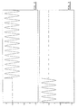
- Figures 2 and 3 show the switching transient for a 1 KHz sinusoid, respectively for a decrement and an increment of the attenuation.
- the method of the invention consists in discriminating between a situation of a commanded increment or decrement of the attenuation and to consequently drive in phase opposition a pair of switches that select the signal path downstream of the selection switch that selects the new required level of attenuation or in other words the particular tap of the resistive voltage divider, producing a rapid closing of the switch. that is selected via software for modifying the attenuation and a slowed down opening of the deselected switch according to a preestablished switch driving ramp.
- the portion or section of the resistive voltage divider pertaining to the commanded change of «tap» turns out to be connected in parallel with a shunt resistance whose value is adequate to sensibly reduce the rate of change of the attenuation according to the voltage ramp that drives the opening of the deselected switch.
- the attenuation network of this invention is characterized by the use of a pair of switches driven in phase opposition by a circuit capable of discriminating between a command of increment of decrement of the attenuation.
- the pair of switches have a current terminal coupled in common to a node of the signal path downstream of the attenuation network, while the other current terminals of the switches are respectively connected to one and to the other end of a second resistive voltage divider having a plurality of taps, respectively connected to the switches for the mutually exclusive selection of the taps of the voltage divider of the attenuator.
- the attenuation network of the invention is characterized by the use of a pair of switches driven in phase opposition (Sup and Sdown), which select the signal path downstream of the tap selection switch (S 0 , S 1 , ..., S 7 ), in function of a logic control signal that discriminates between either an increment or decrement of the attenuation to be implemented by modifying the configuration of the selection switches S 0 , ... S 7 .
- This information or control signal of the pair of switches Sup and Sdown may be easily generated by the digital control system, which receives (either by a command of the operator or by an impulse produced by an automatic control system) a certain instruction for modifying the current configuration of the selection switches S 0 , ... S 7 .
- the driving circuit of the pair of switches Sup and Sdown of the attenuation network of the invention may sense the derivative of the attenuation.
- a circuit is in itself trivial and a thorough illustration thereof is not considered necessary for an exhaustive description of the invention.
- the selection switches S 0 ... S 7 are not connected directly in common to the virtual ground node represented by the input of the output buffer, but instead connected to as many taps or nodes of a series of resistors (R 1 ', R 2 ', R 6 ') that form a chain, or second resistive «voltage divider», connected between the discrimination switches, Sup and Sdown, as shown in the figure.
- a suitable logic circuit command a fast closing of the S 3 switch, while the opening of the S 2 switch is effected by using a relatively slow ramp signal to drive the switch to an OFF state.
- This can usually be implemented by connecting a capacitor of suitable value to a purposely dedicated external pin of the semiconductor device, so that the driving signal of the switch S 2 turns out to be shaped like a ramp, in function of the rise of the voltage on the capacitor (with a certain time constant).
- Any expert technician is conversant with this well known technique that is widely used, for example when implementing a so-called «soft muting» function in audio processors.
- «soft muting function in audio processors.
- FIGs of Fig. 6 show in a schematic way the functioning of the system during a phase of increment of the attenuation.
- Fig. 7 illustrates a simulated switching transient for the case of a sinusoidal signal having a frequency of 1KHz to be subjected to an amplitude variation (attenuation) of 40dB, through a switch (S 2 ) turn-off ramp of 10 milliseconds (ms).
- control circuitry or in other words the circuit that senses the derivative of the attenuation, turns on immediately the switch Sup and simultaneously turns off the switch Sdown.
- Fig. 8 shows the operation in Fig. 8 whereas Fig. 9 shows the switching transient obtained by simulation for the case of a sinusoidal signal having a frequency of 1KHz, undergoing a change of attenuation of 40dB and using a decrement ramp whose duration is 10ms.
- the manner in which the signal for discriminating the direction of the commanded modification of the attenuation level is derived may be different and in any case easily implementable by the use of extremely simple logic circuits.
- the way of generating a turn-off signal for the deselected switch in the form of a ramp of predefinable duration may be different, all being well known and easily realizable by a technician with ordinary knowledge of electronic circuits.
Landscapes
- Networks Using Active Elements (AREA)
- Attenuators (AREA)
Abstract


Description
- The present invention concerns analog circuits for signal processing that are adjustable or automatically controllable by means of digital control circuits. More in particular this invention concerns digitally controlled attenuators.
- In analog signals processors it is often necessary to adjust the signal level, for instance the volume of an audio signal. A remarkable system automation or improved ergonomic criteria of certain manual commands privilege the adoption of digital control techniques of the operation parameters of certain analog circuits of the signal processing system.
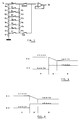
- Typical of these systems, is the employment of digitally controlled attenuators. These are in essence constituted by a voltage divider functionally connected between a first signal input node and a common ground node of the circuit. The voltage divider has a plurality of taps selectable by as many selection switches digitally driven in a mutually exclusive way via software. According to the scheme of Fig. 1, each selectable switch is capable of connecting a certain tap of the voltage divider to a second circuital node (downstream of said first signal input node) of the signal path (for example to the input of an output or coupling buffer). The selection of a particular tap is effected via software command in the form of a «word» composed for example a string of «zeros» and a single «one» that identifies the selected switch. When selecting a different attenuation value, the switches subject to the change of configuration rapidly switch in a mutually exclusive way. The signal is therefore subjected to a higher or lower attenuation in an abrupt manner. When the amplitude variation is relatively large, as in the case of audio systems, this abrupt change may manifest itself by way of a sharp noise (clic). This «switching distortion» is further enhanced when it takes place while the signal is at peak amplitude.
- Figures 2 and 3 show the switching transient for a 1 KHz sinusoid, respectively for a decrement and an increment of the attenuation.
- By referring to the circuit diagram of Fig. 1 and supposing that the system be in the condition (A), having the S2 switch closed along the signal path according to the functional scheme illustrated in Fig. 4, the attenuation in such a condition (A) will be given generally by the following expression:

- When, through the digital control of the switches, the system is commanded in a different condition (B) where the S3 switch is the one «selected», then the attenuation becomes:

- Obviously, a similar amplitude jump occurs when switching over from the condition (B) into the condition (A), as schematically shown in Fig. 4.
- In many cases, specially when the configuration of the digitally controlled attenuator is modified through rather large steps, say of 6 to 10dB, the dynamic distortion that occurs at the switching instant might generate unpleasant audible effects. On the other hand, a more gradual modification of the attenuation might be effected by commanding the execution of a series of attenuation incrementing and decrementing switchings, each switching producing a sufficiently small change of attenuation in order to gradually reach the required (commanded) attenuation level. This system involves a nonnegligible software complication, often incompatible with other requisites of availability of the microprocessor that conducts the execution of adjustment commands for a plurality of functions of the signal processing system.
- In view of these difficulties, a system has now been found for effectively suppressing the dynamic distortion due to a change of configuration of a digitally controlled attenuator that does not require any complication of the software, but rather, is capable of suppressing said distortions substantially via hardware, in an extremely simple way.
- Fundamentally, the method of the invention consists in discriminating between a situation of a commanded increment or decrement of the attenuation and to consequently drive in phase opposition a pair of switches that select the signal path downstream of the selection switch that selects the new required level of attenuation or in other words the particular tap of the resistive voltage divider, producing a rapid closing of the switch. that is selected via software for modifying the attenuation and a slowed down opening of the deselected switch according to a preestablished switch driving ramp. During the opening phase of the switch deselected by the command of modification of the attenuation, the portion or section of the resistive voltage divider pertaining to the commanded change of «tap» turns out to be connected in parallel with a shunt resistance whose value is adequate to sensibly reduce the rate of change of the attenuation according to the voltage ramp that drives the opening of the deselected switch.
- The result of all this is a gradual decrease or increase of the attenuation towards the new value selected by the digital command, obtained via hardware in an extremely simple way.
- The attenuation network of this invention is characterized by the use of a pair of switches driven in phase opposition by a circuit capable of discriminating between a command of increment of decrement of the attenuation. The pair of switches have a current terminal coupled in common to a node of the signal path downstream of the attenuation network, while the other current terminals of the switches are respectively connected to one and to the other end of a second resistive voltage divider having a plurality of taps, respectively connected to the switches for the mutually exclusive selection of the taps of the voltage divider of the attenuator.
- The various aspects of the invention and its advantages will be even more evident through the following description of several embodiments and by referring to the figures herein enclosed, where:
- Figure 1 is a basic circuit diagram of a digitally controlled attenuator, according to the prior art;
- Figures 2 and 3 show the switching transients in one and the other direction of change for a 1KHz sinusoid;
- Figure 4 is an explanatory diagram of the switching mode of the attenuator depicted in Fig. 1 from a condition (A) to a condition (B) and viceversa;
- Figure 5 is a basic circuit diagram of a digitally controlled attenuator made in conformity with the present invention;
- Figures 6 and 7 respectively show the functioning mode and a switching transient in the case of an increment of the attenuation;
- Figure 8 and 9 respectively show the functioning mode and a switching transient in the case of a decrement of the attenuation.
- By referring to Fig. 5, the attenuation network of the invention is characterized by the use of a pair of switches driven in phase opposition (Sup and Sdown), which select the signal path downstream of the tap selection switch (S0, S1, ..., S7), in function of a logic control signal that discriminates between either an increment or decrement of the attenuation to be implemented by modifying the configuration of the selection switches S0, ... S7. This information or control signal of the pair of switches Sup and Sdown, may be easily generated by the digital control system, which receives (either by a command of the operator or by an impulse produced by an automatic control system) a certain instruction for modifying the current configuration of the selection switches S0, ... S7.
- For instance, the driving circuit of the pair of switches Sup and Sdown of the attenuation network of the invention may sense the derivative of the attenuation. Of course, such a circuit is in itself trivial and a thorough illustration thereof is not considered necessary for an exhaustive description of the invention.
- According to the invention, the selection switches S0 ... S7 are not connected directly in common to the virtual ground node represented by the input of the output buffer, but instead connected to as many taps or nodes of a series of resistors (R1', R2', R6') that form a chain, or second resistive «voltage divider», connected between the discrimination switches, Sup and Sdown, as shown in the figure.
- Assume that from a certain level of attenuation, as produced by a configuration where the S2 switch is closed and the others are open, the attenuation must be changed to a higher level by closing the switch S3 and opening the switch S2. The command produced by the digital control system will be such as to determine the Sdown switch to be closed and the Sup switch to be opened. In the above described case, the attenuation for a starting condition (A) will be generally given by the following expression:

- Following to the command of attenuation increment, a suitable logic circuit command a fast closing of the S3 switch, while the opening of the S2 switch is effected by using a relatively slow ramp signal to drive the switch to an OFF state. This can usually be implemented by connecting a capacitor of suitable value to a purposely dedicated external pin of the semiconductor device, so that the driving signal of the switch S2 turns out to be shaped like a ramp, in function of the rise of the voltage on the capacitor (with a certain time constant). Any expert technician is conversant with this well known technique that is widely used, for example when implementing a so-called «soft muting» function in audio processors. Although requiring a dedicated pin, the use of an external capacitor permits to adapt the time constant to the requirements of a particular application. The attenuation network of the invention is such that following to the fast switching on of the switch S3 and until reaching a complete interdiction of the deselected switch S2, the instantaneous value of the attenuation will be given by an expression of the type below:

- By appropriately dimensioning of the resistors R'n of the second or auxiliary voltage divider, it is trivial to impose the following conditions:

- The slow turn-off (opening) of the switch S3 determines a gradual approach toward the imposed new level of attenuation (new condition B), that will be given by the following expression:

- The diagrams of Fig. 6 show in a schematic way the functioning of the system during a phase of increment of the attenuation.
- Fig. 7 illustrates a simulated switching transient for the case of a sinusoidal signal having a frequency of 1KHz to be subjected to an amplitude variation (attenuation) of 40dB, through a switch (S2) turn-off ramp of 10 milliseconds (ms).
- In this case, the control circuitry or in other words the circuit that senses the derivative of the attenuation, turns on immediately the switch Sup and simultaneously turns off the switch Sdown.
- Assuming as a starting condition the one that was attained during the preceding phase of increase of the attenuation, described above and substantially according to which the attenuation (B) is given substantially by the following expression:


- The slow turn-off of the switch S3 determines a gradual reaching of the final value (A) of the attenuation that is given by the following expression:

- Even in this case, the operation is diagrammatically shown in Fig. 8, whereas Fig. 9 shows the switching transient obtained by simulation for the case of a sinusoidal signal having a frequency of 1KHz, undergoing a change of attenuation of 40dB and using a decrement ramp whose duration is 10ms.
- It is evident that the objective of suppressing the dynamic distortion when commanding large attenuation changes is fully met without resorting to a complication of the software and/or to a burdening of the supervising microprocessor but rather by hardware means with a negligible increment of the circuital complexity.
- Moreover, it will be clear to any skilled person that the manner in which the signal for discriminating the direction of the commanded modification of the attenuation level is derived, may be different and in any case easily implementable by the use of extremely simple logic circuits. In addition, the way of generating a turn-off signal for the deselected switch in the form of a ramp of predefinable duration, may be different, all being well known and easily realizable by a technician with ordinary knowledge of electronic circuits.
Claims (5)
- A method for suppressing switching distortion in digitally controlled attenuators constituted by a resistive voltage divider having a plurality of taps that are selectable in a mutually exclusive way via software by a plurality of switches, characterized in that it comprisesdiscriminating between a command of increment or decrement of the attenuation and consequently driving in phase opposition a pair of switches (Sup and Sdown);determining the fast turn-on of the selected one and a slowed down turn-off according to a preestablished driving ramp of the deselected one of said plurality of switches in execution of a command of a change of attenuation;reducing the rate of change of attenuation during said slow turning off of the deselected switch by connecting in parallel to the portion of said resistive voltage divider, pertaining to the change of output tap a shunt resistance which is deselected from the signal path downstream of said selected switch by said pair of switches (Sup and Sdown).
- An attenuation network comprising a first resistive voltage divider coupled to a first node of a signal path and a common ground node and having a plurality of output taps selectable in a mutually exclusive way by a plurality of switches which is configured by a digital datum generated via software, each of said switches coupling a respective tap of said divider to a second node of the signal path, characterized in that comprisesa pair of switches each having a first current terminal coupled in common to said second node and a second current terminal coupled to one and to the other end, respectively, of a second resistive voltage divider having a plurality of taps, each coupled to a respective switch of said plurality of switches for mutually exclusively selecting the taps of said first resistive voltage divider;means for driving in phase opposition said pair of switches in function of a discrimination between an increment or a decrement of the attenuation command;means for turning off the switch of said plurality of switches deselected by the new digital datum through a relatively slow ramp compared with a relatively fast turning on of the switch selected by the new digital datum.
- The attenuation network according to claim 2, characterized in that said means for driving in phase opposition said pair of switches comprise a circuit capable of sensing the sign of the derivative of the attenuation.
- The attenuation network according to claim 2, characterized in that said means for driving in phase opposition said pair of switches comprise a circuit capable of generating a logic signal representative of the direction of change of the attenuation of the contingent command.
- An analog audio processor characterized by comprisinga digitally controlled attenuator constituted by an attenuator network that comprises a pair of switches, each having a first current terminal coupled in common to said second node and a second current terminal coupled to one and to the other end, respectively, of a second resistive voltage divider having a plurality of taps, each coupled to a respective switch of said plurality of switches for mutually exclusively selecting the taps of said first resistive voltage divider;means for driving in phase opposition said pair of switches in function of the result of a discrimination between an attenuation incrementing or decrementing digital command datum;means for turning off the switch of said plurality of switches deselected by the new digital datum through a relatively slow ramp compared with a relatively fast turning on of the switch selected by the new digital datum.
Priority Applications (4)
| Application Number | Priority Date | Filing Date | Title |
|---|---|---|---|
| EP95830304A EP0753937B1 (en) | 1995-07-14 | 1995-07-14 | Method and circuit for the suppression of switching distortion in digitally controlled attenuators |
| DE69528521T DE69528521D1 (en) | 1995-07-14 | 1995-07-14 | Method and circuit for suppressing switching noise in digitally controlled attenuators |
| US08/680,393 US5798959A (en) | 1995-07-14 | 1996-07-15 | Method and device for soft-driving an array of logic gates and suppression of switching distortion |
| JP8205254A JPH0936722A (en) | 1995-07-14 | 1996-07-15 | Method and device to drive array of logical gates softly andmethod of suppressing distortion of switching |
Applications Claiming Priority (1)
| Application Number | Priority Date | Filing Date | Title |
|---|---|---|---|
| EP95830304A EP0753937B1 (en) | 1995-07-14 | 1995-07-14 | Method and circuit for the suppression of switching distortion in digitally controlled attenuators |
Publications (2)
| Publication Number | Publication Date |
|---|---|
| EP0753937A1 true EP0753937A1 (en) | 1997-01-15 |
| EP0753937B1 EP0753937B1 (en) | 2002-10-09 |
Family
ID=8221972
Family Applications (1)
| Application Number | Title | Priority Date | Filing Date |
|---|---|---|---|
| EP95830304A Expired - Lifetime EP0753937B1 (en) | 1995-07-14 | 1995-07-14 | Method and circuit for the suppression of switching distortion in digitally controlled attenuators |
Country Status (2)
| Country | Link |
|---|---|
| EP (1) | EP0753937B1 (en) |
| DE (1) | DE69528521D1 (en) |
Cited By (1)
| Publication number | Priority date | Publication date | Assignee | Title |
|---|---|---|---|---|
| EP3010147A1 (en) * | 2014-10-15 | 2016-04-20 | Analog Devices Global | Apparatus and methods for controlling overshoot in digital step attenuators |
Citations (3)
| Publication number | Priority date | Publication date | Assignee | Title |
|---|---|---|---|---|
| JPS5949009A (en) * | 1982-09-13 | 1984-03-21 | Sanyo Electric Co Ltd | Signal attenuator |
| JPS6093812A (en) * | 1983-10-26 | 1985-05-25 | Nec Corp | Integrated circuit |
| US4683386A (en) * | 1983-07-26 | 1987-07-28 | Nec Corporation | Electronic attenuation value control circuit in which switching noise is suppressed |
-
1995
- 1995-07-14 EP EP95830304A patent/EP0753937B1/en not_active Expired - Lifetime
- 1995-07-14 DE DE69528521T patent/DE69528521D1/en not_active Expired - Lifetime
Patent Citations (3)
| Publication number | Priority date | Publication date | Assignee | Title |
|---|---|---|---|---|
| JPS5949009A (en) * | 1982-09-13 | 1984-03-21 | Sanyo Electric Co Ltd | Signal attenuator |
| US4683386A (en) * | 1983-07-26 | 1987-07-28 | Nec Corporation | Electronic attenuation value control circuit in which switching noise is suppressed |
| JPS6093812A (en) * | 1983-10-26 | 1985-05-25 | Nec Corp | Integrated circuit |
Non-Patent Citations (2)
| Title |
|---|
| PATENT ABSTRACTS OF JAPAN vol. 8, no. 139 (E - 253) 28 June 1984 (1984-06-28) * |
| PATENT ABSTRACTS OF JAPAN vol. 9, no. 244 (E - 346)<1967> 30 September 1985 (1985-09-30) * |
Cited By (2)
| Publication number | Priority date | Publication date | Assignee | Title |
|---|---|---|---|---|
| EP3010147A1 (en) * | 2014-10-15 | 2016-04-20 | Analog Devices Global | Apparatus and methods for controlling overshoot in digital step attenuators |
| US9543921B2 (en) | 2014-10-15 | 2017-01-10 | Analog Devices Global | Apparatus and methods for controlling overshoot in digital step attenuators |
Also Published As
| Publication number | Publication date |
|---|---|
| DE69528521D1 (en) | 2002-11-14 |
| EP0753937B1 (en) | 2002-10-09 |
Similar Documents
| Publication | Publication Date | Title |
|---|---|---|
| US20040178851A1 (en) | AGC circuit | |
| US4068092A (en) | Voice control circuit | |
| US5742899A (en) | Fast attack automatic gain control (AGC) loop for narrow band receivers | |
| US5692017A (en) | Receiving circuit | |
| EP0753937B1 (en) | Method and circuit for the suppression of switching distortion in digitally controlled attenuators | |
| US4276604A (en) | Automatic attenuation circuit | |
| EP0318006A2 (en) | Automatic control system | |
| US5798959A (en) | Method and device for soft-driving an array of logic gates and suppression of switching distortion | |
| EP0464607A2 (en) | Balance control circuit | |
| US5334947A (en) | Logic enhanced noise gate | |
| US4206676A (en) | Electronic musical instrument with sequencer for automatic arpeggio performance | |
| EP0845173B1 (en) | Circuit arrangement for influencing the frequency response of a digital audio signal | |
| US4659996A (en) | Method and apparatus for de-ringing a switched capacitor filter | |
| EP0311031A2 (en) | A method and an electric circuit for controlling an AC-motor, and a circulation pump driven by a motor controlled in this manner | |
| JP3144574B2 (en) | Muting control circuit | |
| US5703956A (en) | External memory control circuit for sound field processing digital signal processor | |
| JPS6165613A (en) | graphite equalizer | |
| JP3064168B2 (en) | Programmable controller | |
| EP0753940A1 (en) | Method and device for softdriving an array of logic gates | |
| JP2847408B2 (en) | Squelch control signal generation circuit | |
| JPH07122972A (en) | Power variable attenuator | |
| KR100539220B1 (en) | Digital controlled Analog Audio Signal Processing Unit Minimizing Signal Distortion | |
| IL48516A (en) | Electrical digital fade in and fade out circuit | |
| JPS5834611A (en) | Electronic volume | |
| US4742251A (en) | Precise call progress detector |
Legal Events
| Date | Code | Title | Description |
|---|---|---|---|
| PUAI | Public reference made under article 153(3) epc to a published international application that has entered the european phase |
Free format text: ORIGINAL CODE: 0009012 |
|
| AK | Designated contracting states |
Kind code of ref document: A1 Designated state(s): DE FR GB IT |
|
| 17P | Request for examination filed |
Effective date: 19970603 |
|
| RAP3 | Party data changed (applicant data changed or rights of an application transferred) |
Owner name: STMICROELECTRONICS S.R.L. |
|
| 17Q | First examination report despatched |
Effective date: 20000519 |
|
| GRAG | Despatch of communication of intention to grant |
Free format text: ORIGINAL CODE: EPIDOS AGRA |
|
| GRAG | Despatch of communication of intention to grant |
Free format text: ORIGINAL CODE: EPIDOS AGRA |
|
| GRAH | Despatch of communication of intention to grant a patent |
Free format text: ORIGINAL CODE: EPIDOS IGRA |
|
| GRAH | Despatch of communication of intention to grant a patent |
Free format text: ORIGINAL CODE: EPIDOS IGRA |
|
| GRAA | (expected) grant |
Free format text: ORIGINAL CODE: 0009210 |
|
| AK | Designated contracting states |
Kind code of ref document: B1 Designated state(s): DE FR GB IT |
|
| PG25 | Lapsed in a contracting state [announced via postgrant information from national office to epo] |
Ref country code: FR Free format text: LAPSE BECAUSE OF FAILURE TO SUBMIT A TRANSLATION OF THE DESCRIPTION OR TO PAY THE FEE WITHIN THE PRESCRIBED TIME-LIMIT Effective date: 20021009 |
|
| REG | Reference to a national code |
Ref country code: GB Ref legal event code: FG4D |
|
| REF | Corresponds to: |
Ref document number: 69528521 Country of ref document: DE Date of ref document: 20021114 |
|
| PG25 | Lapsed in a contracting state [announced via postgrant information from national office to epo] |
Ref country code: DE Free format text: LAPSE BECAUSE OF FAILURE TO SUBMIT A TRANSLATION OF THE DESCRIPTION OR TO PAY THE FEE WITHIN THE PRESCRIBED TIME-LIMIT Effective date: 20030110 |
|
| EN | Fr: translation not filed | ||
| PLBE | No opposition filed within time limit |
Free format text: ORIGINAL CODE: 0009261 |
|
| STAA | Information on the status of an ep patent application or granted ep patent |
Free format text: STATUS: NO OPPOSITION FILED WITHIN TIME LIMIT |
|
| 26N | No opposition filed |
Effective date: 20030710 |
|
| PG25 | Lapsed in a contracting state [announced via postgrant information from national office to epo] |
Ref country code: IT Free format text: LAPSE BECAUSE OF NON-PAYMENT OF DUE FEES;WARNING: LAPSES OF ITALIAN PATENTS WITH EFFECTIVE DATE BEFORE 2007 MAY HAVE OCCURRED AT ANY TIME BEFORE 2007. THE CORRECT EFFECTIVE DATE MAY BE DIFFERENT FROM THE ONE RECORDED. Effective date: 20050714 |
|
| PGFP | Annual fee paid to national office [announced via postgrant information from national office to epo] |
Ref country code: GB Payment date: 20060627 Year of fee payment: 12 |
|
| GBPC | Gb: european patent ceased through non-payment of renewal fee |
Effective date: 20070714 |
|
| PG25 | Lapsed in a contracting state [announced via postgrant information from national office to epo] |
Ref country code: GB Free format text: LAPSE BECAUSE OF NON-PAYMENT OF DUE FEES Effective date: 20070714 |