EP0752288A1 - Composite diamond wire die - Google Patents
Composite diamond wire die Download PDFInfo
- Publication number
- EP0752288A1 EP0752288A1 EP96304785A EP96304785A EP0752288A1 EP 0752288 A1 EP0752288 A1 EP 0752288A1 EP 96304785 A EP96304785 A EP 96304785A EP 96304785 A EP96304785 A EP 96304785A EP 0752288 A1 EP0752288 A1 EP 0752288A1
- Authority
- EP
- European Patent Office
- Prior art keywords
- die
- wire
- diamond
- layer
- substrate
- Prior art date
- Legal status (The legal status is an assumption and is not a legal conclusion. Google has not performed a legal analysis and makes no representation as to the accuracy of the status listed.)
- Withdrawn
Links
Images
Classifications
-
- B—PERFORMING OPERATIONS; TRANSPORTING
- B21—MECHANICAL METAL-WORKING WITHOUT ESSENTIALLY REMOVING MATERIAL; PUNCHING METAL
- B21C—MANUFACTURE OF METAL SHEETS, WIRE, RODS, TUBES, PROFILES OR LIKE SEMI-MANUFACTURED PRODUCTS OTHERWISE THAN BY ROLLING; AUXILIARY OPERATIONS USED IN CONNECTION WITH METAL-WORKING WITHOUT ESSENTIALLY REMOVING MATERIAL
- B21C3/00—Profiling tools for metal drawing; Combinations of dies and mandrels for metal drawing
- B21C3/02—Dies; Selection of material therefor; Cleaning thereof
- B21C3/025—Dies; Selection of material therefor; Cleaning thereof comprising diamond parts
Definitions
- This invention is related generally to diamond dies for wire drawing. More particularly, it is related to a composite diamond die comprising portions made from both chemical vapor deposition (CVD) and natural or high pressure, high temperature (HPHT) diamond.
- CVD chemical vapor deposition
- HPHT high pressure, high temperature
- Wires of metals such as tungsten, copper, iron, molybdenum, and stainless steel are produced by drawing the metals through diamond wire dies.
- Diamond wire dies have been fabricated using single crystal diamonds, however, such dies are difficult to fabricate, tend to chip easily, easily cleave, and often fail catastrophically in use because of the extreme pressures involved during wire drawing.
- Diamond dies which avoid some of the problems attendant with natural diamonds of poorer quality comprise microporous masses compacted from tiny crystals of natural or synthesized diamonds or from crystals of cubic boron nitride.
- the deficiencies of such polycrystalline hard masses are due to the presence of micro-voids/pores and soft inclusions. These voids and inclusions can be more than 10 microns in diameter.
- the improvement of Carrison et al. incorporates an impregnated lubricant in the microporous wire die and a metal cemented carbide jacket to enclose the die.
- European Patent Application 0 494 799 A1 describes a polycrystalline CVD diamond layer having a hole formed therethrough and mounted in a support.
- lines 26-28 "The relatively random distribution of crystal orientations in the CVD diamond ensures more even wear during use of the insert.”
- lines 50-54 "The orientation of the diamond in the polycrystalline CVD diamond layer 10 may be such that most of the crystallites have a (111) crystallographic axis in the plane, i.e. parallel to the surfaces 14, 16, of the layer 10.”
- CVD diamond has been preferred for wire die applications because of its high purity and uniform consistency. Natural diamonds typically are less pure compositionally, and have less morphological consistency. Also, because CVD diamond usually can be produced without attendant voids, it is often more desirable than polycrystalline or single crystal diamond produced by high temperature and high pressure (HPHT) processes. However, the surfaces of CVD diamonds used for wire dies have been observed in some instances to contain to pits or voids after the polishing operations used to form the surfaces of the die, or after wire drawing. These pits or pores may result from the CVD deposition process or from pull-out of fine grains during these operations.
- Pull-out may result from relatively low grain boundary strength, which may in turn be related to the CVD deposition process.
- CVD deposited carbon films are known to contain hydrogen that is bonded to the carbon, particularly in the grain boundaries, which in turn results in a reduction in the number of carbon-carbon bonds across the grain boundaries, and hence, a reduction in the grain boundary strength.
- the degree of pitting observed is greater than that which occurs when natural diamonds that are subject to the same die forming operations.
- Pits or pores are of concern, because they are expected to limit the maximum strength of wire dies in which they occur and, therefore, the types of wire that may be formed in them (e.g. relatively ductile alloys such as many copper alloys versus less ductile alloys, such as most tungsten alloys). Pits or voids may also cause defects in the drawn wire, particularly if they occur in the bearing surface of the die, where most of the wire deformation occurs.
- the present invention may be briefly described as a composite diamond wire die for drawing wire of a predetermined diameter, comprising: a substrate comprising natural or HPHT diamond and having a top surface, a bottom surface and a lateral surface located between the top and bottom surfaces; a layer of CVD diamond deposited on the lateral surface of said substrate (lateral layer); and a wire die bore comprising a wire bearing portion of substantially circular cross-section and a bore axis, said wire die bore extending from the top surface to the bottom surface through the substrate and surrounded by the CVD diamond layer, wherein the circular cross-section of the wire bearing portion is determinative of the diameter of a wire drawn through said wire die bore.
- a wire die of the present invention has a wire die bore extending entirely through the die along a bore axis where the substrate has a ⁇ 110> direction extending substantially parallel to the bore axis.
- the present invention produces a diamond wire die that is less susceptible to voids or pullout within the wire die bore.
- the diamond wire die can draw wire with higher yield strengths than may be drawn with CVD diamond wire dies.
- the diamond wire die is constructed from less costly materials than dies made entirely from single crystal natural diamonds.
- a composite diamond wire die combines the advantages of natural and HPHT diamond with the advantages of CVD diamond.
- a relatively small piece of natural or HPHT diamond is used as a substrate for a layer or layers of CVD diamond.
- the CVD diamond is used to add sufficient material to the substrate to permit the fabrication of a diamond wire die.
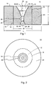
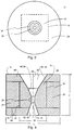
- Fig. 1-3 are cross-sectional and top view illustrations of several embodiments of a composite diamond wire die 10 of the present invention.
- Wire die 10 is for drawing wire (not shown) of a predetermined diameter, and comprises: substrate 12 comprising natural or HPHT diamond and having a top surface 14, bottom surface 16 and lateral surface 18 ; a layer 20 of diamond deposited by chemical vapor deposition (CVD) onto lateral surface 18 of substrate 12 (lateral layer 20); and wire die bore 22 having wire bearing portion 24 of substantially circular cross-section and bore axis 26.
- Wire die bore 22 extends from top surface 14 to bottom surface 16 through substrate 12.
- Wire bearing portion 24 is located completely within substrate 12, and the circular cross-section of wire bearing portion 24 is determinative of the diameter of a wire drawn through the wire die bore 22.
- wire bearing portion 24 comprises a straight bore section 28 having a circular cross-section.
- Wire die bore 22 typically also comprises first taper 30 opening outwardly in one direction from straight bore section 28 toward top surface 14 and second taper 32 opening outwardly in the opposite direction from straight bore section 28 toward second surface 16.
- first taper 30 and second taper 32 are also referred to herein as entrance taper 30 and exit taper 32, respectively.
- a wire to be drawn initially passes through entrance taper 30 where an initial size reduction occurs prior to passing through the straight bore section 28 and exit taper 32.
- approach 36, bearing 38 and exit 40 surfaces correspond to entrance taper 30, wire bearing portion 24 and exit taper 32, respectively.
- Entrance taper 30 typically extends for a greater distance along the direction of bore axis 26 than exit taper 32.
- straight bore portion 28 is closer to bottom surface 16 of wire die 10 than to top surface 14.
- wire die 10 may also comprise top layer 46 and bottom layer 48 of diamond deposited by chemical vapor deposition (CVD) onto first surface 14 and second surface 16 of substrate 12. In such an embodiment, wire die bore 22 will extend through top layer 46 and bottom layer 48.
- Typical wire drawing dies have a disc-shape, although square, hexagonal, octagonal, or other polygonal shapes may be used.
- the length measurement (L) as in the case of a polygonal shape, or the diameter measurement as in the case of a rounded shape, is preferably about 1-20 millimeters. Thicknesses are from 0.3-10 millimeters, with preferred thicknesses being 1-5 millimeters.
- the wire bearing portion 24 suitable for drawing wire is typically from 0.030 mm to 5.0 mm in diameter.
- Wire dies 10, as described herein, may be used to draw wire having desirable uniform properties.
- Wire die 10 may also contain a plurality of wire die bores 22, and these bores may have the same diameters or different diameters.
- Composite diamond wire dies 10 are typically cut from a CVD coated substrate 12.
- conductive CVD diamond layers can be cut by electro-discharge machining, while insulating films can be cut with a laser to form discs, squares, or other symmetrical shapes.
- Wire dies 10 may also be thinned to a preferred thickness, planarized or polished to a particular surface finish. These operations may be done by any suitable method, such as mechanical abrasion, laser polishing, ion thinning, or chemical methods.
- wire die 10 Prior to wire drawing, wire die 10 is mounted in a mechanical support (not shown) of a type well-known in the art in order to provide a means of holding wire die 10 during use and so as to resist axially aligned forces due to wire drawing.
- Substrate 12 may be a natural diamond or a commercially available HPHT sintered diamond (e.g. Compax or Syndite available from the General Electric Company and DeBeers Company, respectively). Substrate 12 is preferably about 0.6-10 mm in width (W), which is about two times the diameter of bore 30. The width and thickness of substrate 12 should be sufficient to contain bore 26. Substrate 12 may have any suitable form, including that of a right circular cylinder or rectangular box. It is preferred that substrate 12 be free from voids and other defects that could result in pull-out in wire bearing portion 24 during wire-drawing. Also, in the case of substrates 12 formed from polycrystalline HPHT diamond, the grain boundary strength should be higher than the yield strength of the wire which is to be drawn.
- substrate 12 comprises a single crystal of natural or HPHT diamond. It is also preferred that the ⁇ 110> direction of the single crystal be oriented such that it is parallel to bore axis 26, because it is well-known that this direction offers the most desirable degree of resistance to wear and abrasion.
- HPHT diamond it may be desirable to form substrate 12 from isotopically pure carbon (carbon consisting of a single isotope). Isotopically pure carbon is known to produce HPHT diamonds with enhanced thermal conductivity, on the order of 33 watts/cm-°K.
- Substrates 12 may also be formed from macles. Macles are naturally occurring thin plates of diamond with a (111) twin plane running parallel to and midway between the main opposing surfaces of the plate. They are found in abundance in alluvial deposits.
- the thickness of substrates 12 of the present invention will range from about 0.1-10 mm. Therefore, the cost of a single crystal or made may be significantly reduced as compared to the cost of a diamond of sufficient quality and thickness necessary to form an entire wire die 10.
- the combination of the thickness of lateral layer 20 should be about 0.4-10 mm, a thickness sufficient to form the balance of the length (L) of wire die 10.
- a preferred technique for forming lateral layer 20 of CVD diamond is set forth in U.S. Patents 5,110,579 and 5387,447, respectively. According to the processes set forth in the U.S patent 5,387,447, diamond is deposited by CVD on a substrate, which in the case of the present invention is also diamond, by a filament process.
- a preferred film comprises substantially transparent columns of diamond crystals having a ⁇ 110> direction perpendicular to the plane of the substrate (parallel to bore axis 26).
- a uniform circumferential CVD coating may be applied to the lateral surface of a substrate. Such a method could be used to form lateral layer 20.
- Grain boundaries between adjacent diamond crystals having hydrogen atoms saturating dangling carbon bonds is preferred, wherein at least 50 percent of the carbon atoms are believed to be tetrahedral bonded based on Raman spectroscopy, infrared and X-ray analysis. It is also contemplated that H, F, Cl, O or other atoms may saturate the dangling carbon bonds.
- the morphology of the CVD layers may also be varied using well known techniques, particularly by controlling the temperature of substrate 12 as the CVD layer is being deposited, as described for example in "Diamond Films 93", Proceedings of the 4th European conference of Diamond, Diamond-like and related Materials, Albufeira, Portugal, Sept. 1993, Editors P.K. Bachmann, I.M. Golden, J.T. Glass and M. Kamo, Publisher: Elsevier Lausanne.
- Possible morphologies include: epitaxial or nearly epitaxial single crystal layers, layers comprising a plurality of large, columnar grains on the order of 50 microns or more, as well as layers that have a grain size that varies through the thickness of the layer, such as layers having a region of smaller grains near lateral surface 14 and a region of larger grains near the outer surface of wire die 10.
- the temperature of substrate 12 during the deposition should be relatively hotter, on the order of 870-1050°C, while smaller grain sizes (e.g. ⁇ 25 microns) require temperatures on the order of 600-850°C.
- a preferred process for making the CVD layers is the filament process described herein. Additional preferred properties of these CVD diamond layers include a thermal conductivity greater than about 4 watts/cm-°K. The thermal conductivity of these CVD films may also be further enhanced by the use of isotopically pure carbonaceous gases for the CVD process, as described in U.S. Patent 5,360,479 to Banholzer et al. The wear resistance and cracking resistance of wire dies 10 increases with increasing thermal conductivity.
- the CVD layer is preferably non-opaque or transparent or translucent and contains hydrogen and oxygen greater than about 1 part per million.
- the diamond film may contain impurities and intentional additives. Impurities may be in the form of catalyst materials, such as iron, nickel, or cobalt.
- Diamond deposition on substrates made of Si, Ge, Nb, V, Ta, Mo, W, Ti, Zr or Hf results in CVD diamond layers that have fewer defects, such as cracks, than other substrates.
- By neutron activation analysis it has been determined that small amounts of these substrate materials are incorporated into the CVD diamond films made on these substrates.
- the CVD layers may contain more than one part per million of a halogen, i.e. fluorine, chlorine, bromine, or iodine.
- Additional additives may include N, B, O, and P which may be present in the form of intentional additives. It is anticipated that CVD layers of the present invention may be made by other known CVD processes, such as microwave CVD processes.
- CVD diamond layers having such preferred conductivity may be produced by other techniques such as microwave CVD and DC jet CVD.
- Intentional additives may include N, S, Ge, Al, and P, each at levels less than 100 ppm. It is contemplated that suitable films may be produced at greater levels. However, lower levels of impurities tend to increase toughness and wear resistance which are very desirable wire die properties. The most preferred films contain less than 5 parts per million and preferably less than 1 part per million impurities and intentional additives.
- CVD layers of the present invention may be deposited so as to contain intrinsic stresses, including intrinsic tensile stresses.
- intrinsic tensile stresses are produced for substrate temperatures during deposition that are greater than about 740°C. The magnitude of these stresses is also known to increase with increasing temperature.
- Tensile stresses in the CVD layer or layers would be expected to place the substrate in compression which is known to be desirable for the purposes of decreasing the possibility of fracture within the wire die, particularly of wire bearing portion 22.
- Wire die bore 26 may be formed by first piercing a pilot hole with a laser and then utilizing an ultrasonically vibrated pin in conjunction with a diamond grit slurry to abrade and form the bore by techniques known in the art.
Landscapes
- Engineering & Computer Science (AREA)
- Mechanical Engineering (AREA)
- Metal Extraction Processes (AREA)
- Crystals, And After-Treatments Of Crystals (AREA)
- Chemical Vapour Deposition (AREA)
Abstract
A composite diamond wire die for drawing wire has a single crystal or HTHP diamond substrate (12) and a CVD layer or layers (20) deposited thereon. The wire die bore (22) extends through the diamond substrate, and the substrate (12) is surrounded by the diamond CVD layer (20).
Description
- This invention is related generally to diamond dies for wire drawing. More particularly, it is related to a composite diamond die comprising portions made from both chemical vapor deposition (CVD) and natural or high pressure, high temperature (HPHT) diamond.
- Wires of metals such as tungsten, copper, iron, molybdenum, and stainless steel are produced by drawing the metals through diamond wire dies. Diamond wire dies have been fabricated using single crystal diamonds, however, such dies are difficult to fabricate, tend to chip easily, easily cleave, and often fail catastrophically in use because of the extreme pressures involved during wire drawing.
- With reference to single crystal diamond wire dies, it is reported in Properties and Applications of Diamond, Wilks et al, Butterworth-Heinemann Ltd 1991, pages 505-507: The best choice of [crystallographic] direction is not too obvious because as the wire passes through the die its circumference is abrading the diamond on a whole 360° range of planes, and the rates of wear on these planes will be somewhat different. Hence, the originally circular hole will not only grow larger but will loose its shape. However, <110> directions offer the advantage that the wire is abrading the sides of the hole with {001} and {011} crystallographic orientations in abrasion resistant directions."
- Diamond dies which avoid some of the problems attendant with natural diamonds of poorer quality comprise microporous masses compacted from tiny crystals of natural or synthesized diamonds or from crystals of cubic boron nitride. The deficiencies of such polycrystalline hard masses, as indicated in U.S. Patent 4,016,736 to Carrison et al., are due to the presence of micro-voids/pores and soft inclusions. These voids and inclusions can be more than 10 microns in diameter. The improvement of Carrison et al. incorporates an impregnated lubricant in the microporous wire die and a metal cemented carbide jacket to enclose the die.
- European Patent Application 0 494 799 A1 describes a polycrystalline CVD diamond layer having a hole formed therethrough and mounted in a support. As set forth in column 2, lines 26-28, "The relatively random distribution of crystal orientations in the CVD diamond ensures more even wear during use of the insert." As set forth in column 3, lines 50-54, "The orientation of the diamond in the polycrystalline
CVD diamond layer 10 may be such that most of the crystallites have a (111) crystallographic axis in the plane, i.e. parallel to thesurfaces layer 10." - Other crystal orientations for CVD films are known. U.S. Patent 5,110,579 to Anthony et al describes a polycrystalline diamond film comprising substantially transparent columns of diamond crystals having a <110> direction perpendicular to the base, as illustrated in Figure 3 of this patent.
- As discussed in, for example, U.S. Patents 5,361,621, 5,363,687 and 5,377,522, CVD diamond has been preferred for wire die applications because of its high purity and uniform consistency. Natural diamonds typically are less pure compositionally, and have less morphological consistency. Also, because CVD diamond usually can be produced without attendant voids, it is often more desirable than polycrystalline or single crystal diamond produced by high temperature and high pressure (HPHT) processes. However, the surfaces of CVD diamonds used for wire dies have been observed in some instances to contain to pits or voids after the polishing operations used to form the surfaces of the die, or after wire drawing. These pits or pores may result from the CVD deposition process or from pull-out of fine grains during these operations. Pull-out may result from relatively low grain boundary strength, which may in turn be related to the CVD deposition process. CVD deposited carbon films are known to contain hydrogen that is bonded to the carbon, particularly in the grain boundaries, which in turn results in a reduction in the number of carbon-carbon bonds across the grain boundaries, and hence, a reduction in the grain boundary strength. The degree of pitting observed is greater than that which occurs when natural diamonds that are subject to the same die forming operations.
- Pits or pores are of concern, because they are expected to limit the maximum strength of wire dies in which they occur and, therefore, the types of wire that may be formed in them (e.g. relatively ductile alloys such as many copper alloys versus less ductile alloys, such as most tungsten alloys). Pits or voids may also cause defects in the drawn wire, particularly if they occur in the bearing surface of the die, where most of the wire deformation occurs.
- Therefore, it is desirable to combine single crystal and CVD diamond to make composite diamond wire dies that take advantage of the properties and characteristics of both.
- The present invention may be briefly described as a composite diamond wire die for drawing wire of a predetermined diameter, comprising: a substrate comprising natural or HPHT diamond and having a top surface, a bottom surface and a lateral surface located between the top and bottom surfaces; a layer of CVD diamond deposited on the lateral surface of said substrate (lateral layer); and a wire die bore comprising a wire bearing portion of substantially circular cross-section and a bore axis, said wire die bore extending from the top surface to the bottom surface through the substrate and surrounded by the CVD diamond layer, wherein the circular cross-section of the wire bearing portion is determinative of the diameter of a wire drawn through said wire die bore.
- In a preferred embodiment, a wire die of the present invention has a wire die bore extending entirely through the die along a bore axis where the substrate has a <110> direction extending substantially parallel to the bore axis.
- The present invention produces a diamond wire die that is less susceptible to voids or pullout within the wire die bore. The diamond wire die can draw wire with higher yield strengths than may be drawn with CVD diamond wire dies. The diamond wire die is constructed from less costly materials than dies made entirely from single crystal natural diamonds.
- A composite diamond wire die combines the advantages of natural and HPHT diamond with the advantages of CVD diamond. A relatively small piece of natural or HPHT diamond is used as a substrate for a layer or layers of CVD diamond. The CVD diamond is used to add sufficient material to the substrate to permit the fabrication of a diamond wire die.
- Embodiments of the invention will now be described, by way of example, with reference to the accompanying drawings, in which:-
- Figs. 1 is a cross-sectional illustrations of a composite diamond wire die of the present invention.
- Fig. 2 is a top view of one embodiment of the wire die of Fig. 1.
- Fig. 3 is a top view of a second embodiment of the wire die of Fig. 1.
- Fig. 4 is a cross-sectional illustration of another embodiment of a composite diamond wire die of the present invention.
- Fig. 1-3 are cross-sectional and top view illustrations of several embodiments of a composite diamond wire die 10 of the present invention. Wire die 10 is for drawing wire (not shown) of a predetermined diameter, and comprises:
substrate 12 comprising natural or HPHT diamond and having atop surface 14,bottom surface 16 andlateral surface 18 ; alayer 20 of diamond deposited by chemical vapor deposition (CVD) ontolateral surface 18 of substrate 12 (lateral layer 20); andwire die bore 22 having wire bearing portion 24 of substantially circular cross-section andbore axis 26.Wire die bore 22 extends fromtop surface 14 tobottom surface 16 throughsubstrate 12. Wire bearing portion 24 is located completely withinsubstrate 12, and the circular cross-section of wire bearing portion 24 is determinative of the diameter of a wire drawn through thewire die bore 22. In a preferred embodiment, wire bearing portion 24 comprises astraight bore section 28 having a circular cross-section.Wire die bore 22 typically also comprisesfirst taper 30 opening outwardly in one direction fromstraight bore section 28 towardtop surface 14 and second taper 32 opening outwardly in the opposite direction fromstraight bore section 28 towardsecond surface 16. As illustrated in Figs. 1-3,first taper 30 and second taper 32 are also referred to herein asentrance taper 30 and exit taper 32, respectively. A wire to be drawn initially passes throughentrance taper 30 where an initial size reduction occurs prior to passing through thestraight bore section 28 and exit taper 32. Referring to diamond wire dies generally, there are four main internal surfaces, commonly identified as theentrance 34, approach 36, bearing 38 and exit 40 surfaces, as shown in Fig. 1. In this description, approach 36, bearing 38 and exit 40 surfaces correspond toentrance taper 30, wire bearing portion 24 and exit taper 32, respectively.Entrance taper 30 typically extends for a greater distance along the direction ofbore axis 26 than exit taper 32. Thus,straight bore portion 28 is closer tobottom surface 16 of wire die 10 than totop surface 14. There is also a wide taper 44 opening ontotop surface 14 that tapers toentrance taper 28. As shown in Fig. 4, wire die 10 may also comprisetop layer 46 andbottom layer 48 of diamond deposited by chemical vapor deposition (CVD) ontofirst surface 14 andsecond surface 16 ofsubstrate 12. In such an embodiment,wire die bore 22 will extend throughtop layer 46 andbottom layer 48. - Typical wire drawing dies have a disc-shape, although square, hexagonal, octagonal, or other polygonal shapes may be used. The length measurement (L) as in the case of a polygonal shape, or the diameter measurement as in the case of a rounded shape, is preferably about 1-20 millimeters. Thicknesses are from 0.3-10 millimeters, with preferred thicknesses being 1-5 millimeters. The wire bearing portion 24 suitable for drawing wire is typically from 0.030 mm to 5.0 mm in diameter. Wire dies 10, as described herein, may be used to draw wire having desirable uniform properties. Wire die 10 may also contain a plurality of
wire die bores 22, and these bores may have the same diameters or different diameters. - Composite
diamond wire dies 10 are typically cut from a CVD coatedsubstrate 12. Preferably, conductive CVD diamond layers can be cut by electro-discharge machining, while insulating films can be cut with a laser to form discs, squares, or other symmetrical shapes. Wire dies 10 may also be thinned to a preferred thickness, planarized or polished to a particular surface finish. These operations may be done by any suitable method, such as mechanical abrasion, laser polishing, ion thinning, or chemical methods. Prior to wire drawing, wire die 10 is mounted in a mechanical support (not shown) of a type well-known in the art in order to provide a means of holding wire die 10 during use and so as to resist axially aligned forces due to wire drawing. -
Substrate 12 may be a natural diamond or a commercially available HPHT sintered diamond (e.g. Compax or Syndite available from the General Electric Company and DeBeers Company, respectively).Substrate 12 is preferably about 0.6-10 mm in width (W), which is about two times the diameter ofbore 30. The width and thickness ofsubstrate 12 should be sufficient to containbore 26.Substrate 12 may have any suitable form, including that of a right circular cylinder or rectangular box. It is preferred thatsubstrate 12 be free from voids and other defects that could result in pull-out in wire bearing portion 24 during wire-drawing. Also, in the case ofsubstrates 12 formed from polycrystalline HPHT diamond, the grain boundary strength should be higher than the yield strength of the wire which is to be drawn. This is to avoid pull-out of grains or failure of the die during use. Preferably,substrate 12 comprises a single crystal of natural or HPHT diamond. It is also preferred that the <110> direction of the single crystal be oriented such that it is parallel to boreaxis 26, because it is well-known that this direction offers the most desirable degree of resistance to wear and abrasion. In the case of HPHT diamond, it may be desirable to formsubstrate 12 from isotopically pure carbon (carbon consisting of a single isotope). Isotopically pure carbon is known to produce HPHT diamonds with enhanced thermal conductivity, on the order of 33 watts/cm-°K. Since the operating temperature of wire bearing portion 24 is one of the most significant determinants of the life of a wire die, the enhanced thermal conductivity of isotopically pure substrates should translate into longer die life than would otherwise be expected for wire dies of the present invention.Substrates 12 may also be formed from macles. Macles are naturally occurring thin plates of diamond with a (111) twin plane running parallel to and midway between the main opposing surfaces of the plate. They are found in abundance in alluvial deposits. Uncoated macles have been used in the past to make wire dies, but they have only been suitable previously for drawing extremely fine wires (e.g., 0.03-0.5 mm in diameter) of relatively ductile material, because of insufficient mechanical strength resulting from their thickness (e.g., 0.1-0.5 mm). Macles are believed to offer an advantage over single crystals for use assubstrate 12, because they have six <110> directions, rather than three as found in single crystals. Thus, wire bearing portion 24 formed from a made would have six-fold rather than three-fold symmetry. Consequently, the wear of wire bearing portion 24 is expected to be more uniform, resulting in longer use of the die before repolishing of the bore. - The thickness of
substrates 12 of the present invention will range from about 0.1-10 mm. Therefore, the cost of a single crystal or made may be significantly reduced as compared to the cost of a diamond of sufficient quality and thickness necessary to form an entire wire die 10. - The combination of the thickness of
lateral layer 20 should be about 0.4-10 mm, a thickness sufficient to form the balance of the length (L) of wire die 10. A preferred technique for forminglateral layer 20 of CVD diamond is set forth in U.S. Patents 5,110,579 and 5387,447, respectively. According to the processes set forth in the U.S patent 5,387,447, diamond is deposited by CVD on a substrate, which in the case of the present invention is also diamond, by a filament process. According to this process, an appropriate gas mixture containing a carbonaceous gas, such as such methane, as set forth in the example, is passed over a heated filament in a sufficient quantity, at a sufficient temperature and for a sufficient length of time to create a diamond layer and build up the layer to a desired thickness. As also described in this patent, a preferred film comprises substantially transparent columns of diamond crystals having a <110> direction perpendicular to the plane of the substrate (parallel to bore axis 26). Such a method may be used to formtop layer 46 andbottom layer 48. As described in the U.S. patent 5,387,447, a uniform circumferential CVD coating may be applied to the lateral surface of a substrate. Such a method could be used to formlateral layer 20. Grain boundaries between adjacent diamond crystals having hydrogen atoms saturating dangling carbon bonds is preferred, wherein at least 50 percent of the carbon atoms are believed to be tetrahedral bonded based on Raman spectroscopy, infrared and X-ray analysis. It is also contemplated that H, F, Cl, O or other atoms may saturate the dangling carbon bonds. - The morphology of the CVD layers may also be varied using well known techniques, particularly by controlling the temperature of
substrate 12 as the CVD layer is being deposited, as described for example in "Diamond Films 93", Proceedings of the 4th European conference of Diamond, Diamond-like and related Materials, Albufeira, Portugal, Sept. 1993, Editors P.K. Bachmann, I.M. Golden, J.T. Glass and M. Kamo, Publisher: Elsevier Lausanne. Possible morphologies include: epitaxial or nearly epitaxial single crystal layers, layers comprising a plurality of large, columnar grains on the order of 50 microns or more, as well as layers that have a grain size that varies through the thickness of the layer, such as layers having a region of smaller grains nearlateral surface 14 and a region of larger grains near the outer surface of wire die 10. To obtain larger grain sizes (e.g. 50 microns) or epitaxial layers, the temperature ofsubstrate 12 during the deposition should be relatively hotter, on the order of 870-1050°C, while smaller grain sizes (e.g. <25 microns) require temperatures on the order of 600-850°C. - A preferred process for making the CVD layers is the filament process described herein. Additional preferred properties of these CVD diamond layers include a thermal conductivity greater than about 4 watts/cm-°K. The thermal conductivity of these CVD films may also be further enhanced by the use of isotopically pure carbonaceous gases for the CVD process, as described in U.S. Patent 5,360,479 to Banholzer et al. The wear resistance and cracking resistance of wire dies 10 increases with increasing thermal conductivity. The CVD layer is preferably non-opaque or transparent or translucent and contains hydrogen and oxygen greater than about 1 part per million. The diamond film may contain impurities and intentional additives. Impurities may be in the form of catalyst materials, such as iron, nickel, or cobalt.
- Diamond deposition on substrates made of Si, Ge, Nb, V, Ta, Mo, W, Ti, Zr or Hf results in CVD diamond layers that have fewer defects, such as cracks, than other substrates. By neutron activation analysis, it has been determined that small amounts of these substrate materials are incorporated into the CVD diamond films made on these substrates. Hence, it may be desirable to adapt the processes described herein to deposit layers that contain between 10 parts per billion and less than 10 parts per million of Si, Ge, Nb, V, Ta, Mo, W, Ti, Zr or Hf. Additionally, the CVD layers may contain more than one part per million of a halogen, i.e. fluorine, chlorine, bromine, or iodine. Additional additives may include N, B, O, and P which may be present in the form of intentional additives. It is anticipated that CVD layers of the present invention may be made by other known CVD processes, such as microwave CVD processes.
- It is also contemplated that CVD diamond layers having such preferred conductivity may be produced by other techniques such as microwave CVD and DC jet CVD. Intentional additives may include N, S, Ge, Al, and P, each at levels less than 100 ppm. It is contemplated that suitable films may be produced at greater levels. However, lower levels of impurities tend to increase toughness and wear resistance which are very desirable wire die properties. The most preferred films contain less than 5 parts per million and preferably less than 1 part per million impurities and intentional additives.
- It is also well-known that CVD layers of the present invention may be deposited so as to contain intrinsic stresses, including intrinsic tensile stresses. For the method of deposition described herein, intrinsic tensile stresses are produced for substrate temperatures during deposition that are greater than about 740°C. The magnitude of these stresses is also known to increase with increasing temperature. Tensile stresses in the CVD layer or layers would be expected to place the substrate in compression which is known to be desirable for the purposes of decreasing the possibility of fracture within the wire die, particularly of
wire bearing portion 22. - Wire die bore 26 may be formed by first piercing a pilot hole with a laser and then utilizing an ultrasonically vibrated pin in conjunction with a diamond grit slurry to abrade and form the bore by techniques known in the art.
Claims (11)
- A composite diamond wire die for drawing wire of a predetermined diameter, comprising:a substrate comprising natural or HPHT diamond and having a top surface, a bottom surface and a lateral surface located between the top and bottom surfaces;a lateral layer of CVD diamond, deposited on the lateral surface of said substrate; anda wire die bore comprising a wire bearing portion of substantially circular cross-section and a bore axis, said wire die bore extending from the top surface to the bottom surface through the substrate and surrounded by the CVD diamond layer, wherein the circular cross-section of the wire bearing portion is determinative of the diameter of a wire drawn through said wire die bore.
- The die of claim 1, wherein the morphology of said lateral layer of CVD diamond comprises: 1) a region of smaller grains adjacent to said substrate and a region of larger grains adjacent to an outer surface of said lateral layer, or 2) a plurality of large, columnar grains, or 3) an epitaxial layer.
- The die of claim 2, wherein said lateral layer comprises a plurality of large, columnar grains that are transparent, semi-transparent, translucent, or non-opaque.
- The die of any one of claims 1 to 3, wherein said lateral layer of CVD diamond contains intrinsic tensile stresses.
- The die of any one of claims 1 to 4, further comprising a top layer and a bottom layer of CVD diamond deposited on the top surface and the bottom surface, respectively, of the substrate, wherein a portion of said bore extends through both the top and bottom layers.
- The die of claim 5, wherein both said top and bottom layers of CVD diamond contain intrinsic tensile stresses.
- The die of any one of claims 1 to 6, wherein said substrate, said lateral layer or both are formed from an isotopically pure carbonaceous material.
- The die of any one of claims 1 to 7, wherein said lateral layer is transparent, translucent or non-opaque and contains hydrogen and oxygen in a concentration greater than about 1 ppm.
- The die of any one of claims 1 to 7, wherein said lateral layer contains less than 1 ppm of impurities and intentional additives.
- The die of any one of claims 1 to 7, wherein said lateral layer contains more than 1 ppm of a halogen comprising fluorine, chlorine, bromine, or iodine.
- The die of any one of claims 1 to 10, wherein said lateral layer comprises a microstructure having grain boundaries, the grain boundaries comprising hydrogen saturated dangling carbon bonds.
Applications Claiming Priority (2)
| Application Number | Priority Date | Filing Date | Title |
|---|---|---|---|
| US08/499,502 US5634370A (en) | 1995-07-07 | 1995-07-07 | Composite diamond wire die |
| US499502 | 1995-07-07 |
Publications (1)
| Publication Number | Publication Date |
|---|---|
| EP0752288A1 true EP0752288A1 (en) | 1997-01-08 |
Family
ID=23985506
Family Applications (1)
| Application Number | Title | Priority Date | Filing Date |
|---|---|---|---|
| EP96304785A Withdrawn EP0752288A1 (en) | 1995-07-07 | 1996-06-28 | Composite diamond wire die |
Country Status (4)
| Country | Link |
|---|---|
| US (1) | US5634370A (en) |
| EP (1) | EP0752288A1 (en) |
| JP (1) | JPH09122739A (en) |
| KR (1) | KR970005429A (en) |
Cited By (2)
| Publication number | Priority date | Publication date | Assignee | Title |
|---|---|---|---|---|
| WO2004074557A1 (en) * | 2003-02-19 | 2004-09-02 | Element Six Limited | Cvd diamond in wear applications |
| CN104789937A (en) * | 2015-02-15 | 2015-07-22 | 河北一缆通电子商务有限公司 | Production method for drawing mold with nano-scale diamond coating on inner hole surface |
Families Citing this family (6)
| Publication number | Priority date | Publication date | Assignee | Title |
|---|---|---|---|---|
| JP3885293B2 (en) * | 1997-06-25 | 2007-02-21 | 住友電気工業株式会社 | Diamond indenter |
| US5957005A (en) * | 1997-10-14 | 1999-09-28 | General Electric Company | Wire drawing die with non-cylindrical interface configuration for reducing stresses |
| KR100438401B1 (en) * | 2001-08-14 | 2004-07-02 | 김기열 | Under-floor heating system panel for boiler |
| JP5289753B2 (en) * | 2007-11-12 | 2013-09-11 | 株式会社フジクラ | Deformed dies and extra fine deformed wires manufactured using them |
| KR101186165B1 (en) * | 2012-02-06 | 2012-10-02 | 한국과학기술연구원 | Polycrystalline diamond for drawing dies and method for fabricating the same |
| WO2020004373A1 (en) * | 2018-06-27 | 2020-01-02 | 住友電工ハードメタル株式会社 | Tool with through hole, diamond component, and diamond material |
Citations (2)
| Publication number | Priority date | Publication date | Assignee | Title |
|---|---|---|---|---|
| EP0024757A1 (en) * | 1979-08-23 | 1981-03-11 | General Electric Company | Diamond compacts and tools containing them |
| EP0531085A2 (en) * | 1991-09-03 | 1993-03-10 | General Electric Company | Isotopic diamond coated products and their production |
Family Cites Families (17)
| Publication number | Priority date | Publication date | Assignee | Title |
|---|---|---|---|---|
| DE1452389A1 (en) * | 1965-08-02 | 1968-11-28 | Mannesmann Ag | Die for extrusion of metals |
| US3831428A (en) * | 1973-03-26 | 1974-08-27 | Gen Electric | Composite wire drawing die |
| US4016736A (en) * | 1975-06-25 | 1977-04-12 | General Electric Company | Lubricant packed wire drawing dies |
| US4303442A (en) * | 1978-08-26 | 1981-12-01 | Sumitomo Electric Industries, Ltd. | Diamond sintered body and the method for producing the same |
| NL7904922A (en) * | 1979-06-25 | 1980-12-30 | Philips Nv | METHOD FOR MANUFACTURING A DRAWING STONE. |
| US4462242A (en) * | 1980-03-10 | 1984-07-31 | Gk Technologies, Incorporated | Method for wire drawing |
| IE57439B1 (en) * | 1985-04-09 | 1992-09-09 | De Beers Ind Diamond | Wire drawing die |
| US5273731A (en) * | 1989-09-14 | 1993-12-28 | General Electric Company | Substantially transparent free standing diamond films |
| US5110579A (en) * | 1989-09-14 | 1992-05-05 | General Electric Company | Transparent diamond films and method for making |
| CA2030049A1 (en) * | 1989-12-11 | 1991-06-12 | Thomas R. Anthony | Single-crystal diamond of very high thermal conductivity |
| US5360479A (en) * | 1990-07-02 | 1994-11-01 | General Electric Company | Isotopically pure single crystal epitaxial diamond films and their preparation |
| GB9100631D0 (en) * | 1991-01-11 | 1991-02-27 | De Beers Ind Diamond | Wire drawing dies |
| CA2087765A1 (en) * | 1992-02-07 | 1993-08-08 | David E. Slutz | Method for producing uniform cylindrical tubes of cvd diamond |
| US5363687A (en) * | 1993-09-14 | 1994-11-15 | General Electric Company | Diamond wire die |
| US5377522A (en) * | 1993-10-27 | 1995-01-03 | General Electric Company | Diamond wire die with positioned opening |
| US5361621A (en) * | 1993-10-27 | 1994-11-08 | General Electric Company | Multiple grained diamond wire die |
| JP3250696B2 (en) * | 1993-12-27 | 2002-01-28 | 本田技研工業株式会社 | Mold manufacturing method |
-
1995
- 1995-07-07 US US08/499,502 patent/US5634370A/en not_active Expired - Fee Related
-
1996
- 1996-06-28 EP EP96304785A patent/EP0752288A1/en not_active Withdrawn
- 1996-06-28 JP JP8168072A patent/JPH09122739A/en not_active Withdrawn
- 1996-07-06 KR KR1019960027347A patent/KR970005429A/en not_active Withdrawn
Patent Citations (2)
| Publication number | Priority date | Publication date | Assignee | Title |
|---|---|---|---|---|
| EP0024757A1 (en) * | 1979-08-23 | 1981-03-11 | General Electric Company | Diamond compacts and tools containing them |
| EP0531085A2 (en) * | 1991-09-03 | 1993-03-10 | General Electric Company | Isotopic diamond coated products and their production |
Cited By (5)
| Publication number | Priority date | Publication date | Assignee | Title |
|---|---|---|---|---|
| WO2004074557A1 (en) * | 2003-02-19 | 2004-09-02 | Element Six Limited | Cvd diamond in wear applications |
| GB2415189A (en) * | 2003-02-19 | 2005-12-21 | Element Six Ltd | Cvd diamond in wear applications |
| GB2415189B (en) * | 2003-02-19 | 2007-09-26 | Element Six Ltd | Cvd diamond in wear applications |
| US7799427B2 (en) | 2003-02-19 | 2010-09-21 | Element Six Limited | CVD diamond in wear applications |
| CN104789937A (en) * | 2015-02-15 | 2015-07-22 | 河北一缆通电子商务有限公司 | Production method for drawing mold with nano-scale diamond coating on inner hole surface |
Also Published As
| Publication number | Publication date |
|---|---|
| US5634370A (en) | 1997-06-03 |
| KR970005429A (en) | 1997-02-19 |
| JPH09122739A (en) | 1997-05-13 |
Similar Documents
| Publication | Publication Date | Title |
|---|---|---|
| US5465603A (en) | Optically improved diamond wire die | |
| US11739419B2 (en) | Highly adhesive CVD grown boron doped diamond graded layer on WC-Co | |
| EP3369492B1 (en) | Wear-resistant tool | |
| US11684981B2 (en) | Ultra-fine nanocrystalline diamond precision cutting tool and manufacturing method therefor | |
| US5634370A (en) | Composite diamond wire die | |
| US6267867B1 (en) | Composite article with adherent CVD diamond coating and method of making | |
| EP0569117A2 (en) | Producing articles by chemical vapor deposition | |
| Lavrinenko | CVD diamonds in diamond tools: features and properties, peculiarities of processing, and application in modern diamond tools | |
| US5636545A (en) | Composite diamond wire die | |
| EP0652058B1 (en) | Diamond wire die with positioned opening | |
| US5634369A (en) | Composite diamond wire die | |
| US5858480A (en) | Ceramic-based substrate for coating diamond and method for preparing substrate for coating | |
| US5363687A (en) | Diamond wire die | |
| EP0652057B1 (en) | Multiple grained diamond wire die | |
| US5571236A (en) | Diamond wire drawing die | |
| US5551277A (en) | Annular diamond bodies | |
| JP2002540970A (en) | Diamond coated tool and method of making same | |
| Taher et al. | Effect of methane concentration on mechanical properties of HFCVD diamond-coated cemented carbide tool inserts | |
| Peng et al. | Characterization and adhesion strength of diamond films deposited on silicon nitride inserts by dc plasma jet chemical vapour deposition | |
| JPH1158106A (en) | Diamond coated cutting tool and its manufacturing method | |
| CN114606465A (en) | Method for producing cutting wire and cutting wire | |
| Shi et al. | Growth of a well-adhering diamond coating on sintered tungsten | |
| JP3671143B2 (en) | Chemical vapor deposition diamond product and method for producing the same | |
| KR960007380B1 (en) | Diamond-coated hard material and its manufacturing method | |
| JPH09220610A (en) | Wire drawing die for fine wire using polycrystalline diamond synthesized by vapor phase method |
Legal Events
| Date | Code | Title | Description |
|---|---|---|---|
| PUAI | Public reference made under article 153(3) epc to a published international application that has entered the european phase |
Free format text: ORIGINAL CODE: 0009012 |
|
| AK | Designated contracting states |
Kind code of ref document: A1 Designated state(s): BE DE ES FR GB IT |
|
| 17P | Request for examination filed |
Effective date: 19970708 |
|
| 17Q | First examination report despatched |
Effective date: 20000225 |
|
| STAA | Information on the status of an ep patent application or granted ep patent |
Free format text: STATUS: THE APPLICATION IS DEEMED TO BE WITHDRAWN |
|
| 18D | Application deemed to be withdrawn |
Effective date: 20000707 |