EP0749205A1 - Verstärkerstufe mit geschalteten Kapazitäten - Google Patents
Verstärkerstufe mit geschalteten Kapazitäten Download PDFInfo
- Publication number
- EP0749205A1 EP0749205A1 EP96109157A EP96109157A EP0749205A1 EP 0749205 A1 EP0749205 A1 EP 0749205A1 EP 96109157 A EP96109157 A EP 96109157A EP 96109157 A EP96109157 A EP 96109157A EP 0749205 A1 EP0749205 A1 EP 0749205A1
- Authority
- EP
- European Patent Office
- Prior art keywords
- capacitor
- terminal
- coupled
- amplifier
- input
- Prior art date
- Legal status (The legal status is an assumption and is not a legal conclusion. Google has not performed a legal analysis and makes no representation as to the accuracy of the status listed.)
- Granted
Links
Images


Classifications
-
- H—ELECTRICITY
- H03—ELECTRONIC CIRCUITRY
- H03M—CODING; DECODING; CODE CONVERSION IN GENERAL
- H03M1/00—Analogue/digital conversion; Digital/analogue conversion
- H03M1/12—Analogue/digital converters
- H03M1/34—Analogue value compared with reference values
- H03M1/38—Analogue value compared with reference values sequentially only, e.g. successive approximation type
- H03M1/44—Sequential comparisons in series-connected stages with change in value of analogue signal
- H03M1/442—Sequential comparisons in series-connected stages with change in value of analogue signal using switched capacitors
-
- H—ELECTRICITY
- H03—ELECTRONIC CIRCUITRY
- H03F—AMPLIFIERS
- H03F3/00—Amplifiers with only discharge tubes or only semiconductor devices as amplifying elements
- H03F3/005—Amplifiers with only discharge tubes or only semiconductor devices as amplifying elements using switched capacitors, e.g. dynamic amplifiers; using switched capacitors as resistors in differential amplifiers
-
- H—ELECTRICITY
- H03—ELECTRONIC CIRCUITRY
- H03H—IMPEDANCE NETWORKS, e.g. RESONANT CIRCUITS; RESONATORS
- H03H19/00—Networks using time-varying elements, e.g. N-path filters
- H03H19/004—Switched capacitor networks
Definitions
- This invention relates, in general, to gain stages, and more particularly, to switched capacitor gain stages.
- An amplifier typically has an input and an output.
- the amplifier amplifies a signal applied to the input and provides the amplified signal at the output.
- amplifiers are characterized by the amount of gain or amplification provided, bandwidth or frequency of operation, noise characteristics, and accuracy of amplification.
- Amplifiers are commonly used in many different types of circuits, for example, Analog to Digital converters.
- a switched capacitor amplifier is a clocked circuit that operates in discrete steps. For example, in a first phase of a clock cycle a voltage is sampled, in particular, capacitors of a switched capacitor amplification stage are charged to the voltage. Switches are used to couple the capacitors in different configurations. The switches are transmission gates formed from complementary transistor types. In a second phase of a clock cycle, the capacitors of the switched capacitor amplifier are coupled via switches around an amplifier in a configuration to amplify a sampled voltage. The voltages stored on the capacitors in the first phase of the clock cycle determine the magnitude of an output voltage of the amplification stage. The gain is typically fixed by the amplification stage configuration (in the second phase of the clock cycle) and the capacitor values.
- the operational speed of a switched capacitor amplifier stage is limited by the time needed to charge and discharge capacitors of the amplifier stage or the time required for an amplifier of the amplification stage to stabilize.
- switched capacitor gain staged are used in pipelined Analog to Digital Converter (ADC) stages.
- the switched capacitor gain stages are used in a pipelined ADC to amplify an analog signal.
- An output of a switched capacitor gain stage in an ADC corresponds to a digital equivalent of an analog signal level.
- the speed or frequency at which an analog signal can be converted to a digital signal is directly related to the speed of the switched capacitor amplifier stages.
- An increase in the speed of switched capacitor amplifiers stages of an analog to digital converter can be used to enhance the frequency of operation.
- An amplifier is an essential component of an Analog to Digital Converter (ADC).
- ADC Analog to Digital Converter
- ADC Analog to Digital Converter
- a pipelined ADC employs a group of series coupled amplifier stages for generating a digital signal.
- An amplifier stage is susceptible to producing error due to capacitor mismatch, voltage offset of the amplifier, non-ideal switches, noise, finite amplifier gain, finite amplifier bandwidth, and device leakage. Any error produced by an amplifier stage degrades the performance of the ADC.
- FIG. 1 is a block diagram of a pipelined Analog to Digital Converter (ADC) 11.
- ADC 11 has an input for receiving an analog signal and an output for providing a digital output signal.
- Amplifier gain stages 12 are coupled in series, each generating a digital signal corresponding to a magnitude of the sampled analog signal.
- An alignment and synchronization circuit 13 coordinates the digital conversion process.
- a pipelined ADC samples an analog signal at a specified clock rate and generates a digital signal corresponding to a voltage magnitude of each sampled signal.
- the resolution or accuracy of a pipelined ADC is a function of the number of amplifier gain stages used. Each series coupled amplifier gain stage corresponds to a bit of resolution, starting with the Most Significant Bit (MSB) for a first stage of amplification and ending with the Least Significant Bit (LSB) for a last stage of amplification.
- MSB Most Significant Bit
- LSB Least Significant Bit
- ADC 11 The speed of operation of ADC 11 is directly related to the speed of the series coupled amplifier gain stages 12. Each amplifier gain stage relies on the results of a preceding amplifier gain stage before generating a digital signal.
- An amplifier gain stage includes a switched capacitor gain stage and at least one comparator.
- a switched capacitor gain stage of an amplifier gain stage amplifies a voltage received by the amplifier gain stage which is coupled to an adjacent amplifier gain stage.
- a comparator of an amplifier gain stage compares the voltage received by the amplifier gain stage against a reference voltage and generates a corresponding logic level.
- the clock rate at which an input signal is sampled by ADC 11 is determined by the delay path through amplifier gain stages 12 and delay due to alignment and synchronization circuit 13. Accordingly, the clock rate could be increased if the operating speed of amplifier gain stages 12 is reduced.
- amplifier gain stages 12 of pipelined ADC 11 have a gain of two.
- a reference voltage (Vref) is either added to or subtracted from an amplified voltage of a first amplifier gain stage (Gain Stage 1 of FIG. 1) depending on the comparison results.
- a logic level is also set based on the comparison results.
- a resulting output voltage (2*Vin +/-Vref) is then applied to a next amplification stage (Gain Stage 2 of FIG. 1) and the process is repeated such that the sample voltage is pipelined to determine the remaining digital bits sequentially as is well known.
- Each of the pipelined ADC circuits listed hereinabove utilize a group of series coupled amplifier gain stages.
- the amplifiers stages described in the articles are switched capacitor amplifier stages that have similar characteristics.
- the switched capacitor amplifier stages are a clocked circuit. Capacitors of the switched capacitor circuit are charged during a first phase of a clock cycle. The capacitors are then coupled around an operational amplifier in a predetermined configuration during a second phase of the clock cycle.
- the speed of operation of a switched capacitor amplifier stage is increased by a factor of two by utilizing an amplifier of the switched capacitor amplifier stage during the complete clock cycle instead of one half the clock cycle as stated above.
- Two groups or sets of capacitors are switched in and out to continuously amplify sampled signals.
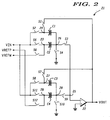
- FIG. 2 is a schematic diagram illustrating a switched capacitor amplifier stage 21 in accordance with the present invention.
- Switched capacitor amplifier stage 21 comprises switches S1-S12, capacitors C1-C4 and an amplifier stage 22. Switches S1-S6 and capacitors C1 and C2 with amplifier 22 during one phase of a clock cycle. Switches S7-S12 operate with amplifier 22 during the other phase of the clock cycle.
- Switched capacitor amplifier stage 21 has an input VIN, an input VREFP, an input VREFM, and an output VOUT. Inputs VREFM and VREFP are inputs for respectively subtracting a reference voltage from the amplified signal at VOUT of switched capacitor amplifier stage 21.
- Amplifier 22 has an inverting input coupled to a node 25, a non-inverting input coupled to a power supply terminal (e.g. ground), and an output coupled to the output VOUT.
- Switch S1 couples between output VOUT and a node 24.
- Switch S2 couples between input VIN and node 24.
- Switch S3 couples between a node 26 and a node 25.
- Switch S4 couples between node 26 and the power supply terminal (e.g. ground).
- Switch S5 couples between inputs VIN and a node 23.
- Switch S6 couples between input VREFM and node 23.
- Capacitor C1 couples between node 24 and node 26.
- Capacitor C2 couples
- Switches S2, S5, and S4 couple capacitors C1 and C2 between the input VIN and ground. Switches S2, S5, and S4 allow capacitors C1 and C2 to charge to a voltage applied to VIN.
- Switches S1 and S3 couple capacitor C1 between the inverting input and the output of amplifier 22.
- Switches S6 and S3 couple capacitor C2 between the input VREFM and the inverting input of amplifier 22.
- a reference voltage applied to VREFM is subtracted from an output voltage at the output VOUT when capacitors C1 and C2 are coupled around amplifier 22.
- Switch S7 couples between a node 27 and the output VOUT.
- Switch S8 couples between the input VIN and node 27.
- Switch S9 couples between a node 29 and node 25.
- Switch S10 couples between node 29 and the power supply terminal (e.g. ground).
- Switch S11 couples between the input VIN and a node 28.
- Switch S12 couples between the input VREFP and node 28.
- Capacitor C3 couples between node 27 and node 29.
- Capacitor C4 couples between node 28 and node 29.
- Switches S8, S10, and S11 couple capacitors C3 and C4 between the input VIN and ground. Switches S8, S10, and S11 allow capacitors C3 and C4 to charge to a voltage applied to VIN.
- Switches S7 and S9 couple capacitor C3 between the inverting input and the output of amplifier 22.
- Switches S12 and S9 couple capacitor C4 between the input VREFP and the inverting input of amplifier 22.
- a reference voltage applied to VREFP is subtracted from an output voltage at the output VOUT when capacitors C3 and C4 are coupled around amplifier 22.
- FIG. 3 is a timing diagram illustrating clock signals for opening and closing switches S1-S12 of switched capacitor amplifier stage 21 of FIG. 2.
- a clock signal CLK1 and a clock signal CLK1BAR are used to enable and disable switches S1-S12.
- CLK1BAR is the complement of the clock signal CLK1.
- the rate of sampling is doubled by sampling and providing an output signal during either phase of the clock signal CLK1. Double sampling makes an effective clock rate of switched capacitor amplifier stage 21 of FIG. 2 equal to twice the frequency of clock signal CLK1 since an output signal is provided during each clock phase.
- the clock signals CLK1 and CLK1BAR are non-overlapping.
- FIG. 4 is a schematic diagram of capacitors C1 and C2 of switched capacitor amplifier stage 21 of FIG. 2 when the clock signal CLK1 of FIG. 3 is at a logic one level and the clock signal CLK1BAR of FIG. 3 is at a logic zero level.
- Capacitors C1 and C2 are in a sampling configuration. Switches S2, S4, and S5 are closed thereby coupling capacitors C1 and C2 between the input VIN and ground. A voltage applied to the input VIN charges capacitors C1 and C2. Note that charging capacitors C1 and C2 works independent of amplifier 22 of FIG. 2.
- FIG. 5 is a schematic diagram of capacitors C1 and C2 in a gain configuration around switched capacitor amplifier stage 21 of FIG. 2 when the clock signal CLK1 of FIG. 3 is at a logic zero level and the clock signal CLK1BAR of FIG. 3 is at a logic one level.
- Switches S1, S3, and S6 are closed.
- Capacitor C1 is coupled between the inverting input and the output of amplifier 22.
- Capacitor C2 is coupled between the input VREFM and the inverting input of amplifier 22.
- capacitors C1 and C2 have an equal capacitance which configures the amplifier stage in a gain of two.
- a reference voltage applied to VREFM subtracts from an amplified voltage of a sampled voltage on capacitors C1 and C2.
- the amplifier stage shown in FIG. 5 multiplies the voltage sampled in FIG. 4 on capacitors C1 and C2 by a factor of two and subtracts out the reference voltage applied to VREFM.
- FIG. 6 is a schematic diagram of capacitors C3 and C4 of switched capacitor amplifier stage 21 of FIG. 2 when the clock signal CLK1 of FIG. 3 is at a logic zero level and the clock signal CLK1 BAR of FIG. 3 is at a logic one level.
- Capacitors C3 and C4 are in a sampling configuration. Switches S8, S10, and S11 are closed thereby coupling capacitors C3 and C4 between the input VIN and ground. A voltage applied to the input VIN charges capacitors C3 and C4. Note that charging capacitors C3 and C4 works independent of amplifier 22 of FIG. 2. Capacitors C3 and C4 are being charged when capacitors C1 and C2 of FIG. 2 are in a gain configuration around amplifier 22 of FIG. 2.
- FIG. 7 is a schematic diagram of capacitors C3 and C4 in a gain configuration around switched capacitor amplifier stage 21 of FIG. 2 when the clock signal CLK1 of FIG. 3 is at a logic one level and the clock signal CLK1BAR of FIG. 3 is at a logic zero level.
- Switches S7, S9, and S12 are closed.
- Capacitor C3 is coupled between the inverting input and the output of amplifier 22 of FIG. 2.
- Capacitor C4 is coupled between the input VREFP and the inverting input of amplifier 22.
- capacitors C3 and C4 have an equal capacitance which configures the amplifier stage in a gain of two.
- a reference voltage applied to VREFP subtracts from an amplified voltage of a sampled voltage on capacitors C3 and C4.
- the switched capacitor amplifier stage shown in FIG. 7 multiplies the voltage sampled in FIG. 6 on capacitors C3 and C4 by a factor of two and subtracts out the reference voltage applied to VREFP.
- Capacitors C1 and C2 of FIG. 2 are being charged when capacitors C3 and C4 are in a gain configuration around amplifier 22.
- Switched capacitor amplifier stage 21 provides an output signal at twice the rate of prior art amplifier stages that sample during a first phase of a clock signal and amplify during a second phase of the clock signal. Additional capacitors are added for sampling during both clock phases of a clock signal.
- Prior art amplifier stages have a dead period during a clock half cycle when capacitors of an amplifier stage are charged and the amplifier is not used. Performance of an amplifier is degraded if it is continuously turned on and off with each half cycle due to the extra time required for the amplifier to stabilize to a quiescent state.
- Prior art amplifier stages eliminate this problem by adding dummy switches and capacitors to provide feedback to the amplifier during the portion of the clock cycle that the amplifier is not used.
- the circuit shown in FIG. 2 does not have the problem of a period when the amplifier is not used since amplifier 22 of FIG. 2 is operated continuously during a clock cycle. No dummy switches and capacitors which increase the area of the circuit are needed. The only break in operation is when one group of capacitors is being decoupled from an amplifier for sampling a voltage and the other group of capacitors is being coupled in a gain configuration around the amplifier or vice versa.
- Switched capacitor amplifier stage 22 of FIG. 2 reduces power reduction by a factor of two when operated at similar speeds as the prior art amplifier stages described hereinabove.
- Switched capacitor amplifier stage 22 can operate at one half the frequency of a single sampling amplifier stage, thus it will dissipate one half the power. Also, amplifier loading is close to prior art amplifier stages.
- FIG. 8 is a switched capacitor amplifier stage 71 in a fully differential configuration corresponding to the switched capacitor amplifier stage 21 of FIG. 2.
- a fully differential configuration of an amplifier stage is beneficial ford the rejection of noise that is common to both inputs and doubles the achievable dynamic range.
- Switched capacitor amplifier stage 71 has an input A, an input B, an input VREFMA, an input VREFMB, an input VREFPA, an input VREFPB, an output A, and an output B. Operation of switched capacitor amplifier stage 71 is similar to that described for switched capacitor amplifier stage 21 of FIG. 2. A difference is that the capacitors and switches coupled around the inverting input of amplifier 22 of FIG. 2 is duplicated for the non-inverting input of switched capacitor amplifier stage 71.
- Capacitors C1-C4 and switches coupled thereto correspond to a first sampling circuit for an amplifier 72.
- Capacitors C1 and C2 receive a voltage from input A.
- Capacitors C3 and C4 receive a voltage from input B. The voltage difference between inputs A and B are amplified by an amplifier 72.
- Capacitors C5-C8 and switches coupled thereto correspond to a second sampling circuit for amplifier 72.
- Capacitors C5 and C6 receive a voltage from input A.
- Capacitors C7 and C8 receive a voltage at input B.
- Capacitors C1-C4 are charged to a voltage (between inputs A and B, and ground) during a first clock phase while capacitors C5-C8 are coupled around amplifier 72 in a gain configuration similar to that shown in FIGs 5 and 6.
- a differential reference voltage is applied across inputs VREFPA and VREFPB.
- capacitors C5-C8 are charged to a voltage (between inputs A and B, and ground) while capacitors C1-C4 are coupled around amplifier 72 in a gain configuration.
- a differential reference voltage is applied across inputs VREFMA and VREFMB.
- Amplifier 72 is operated throughout the clock cycle due to the double sampling process. Although more circuitry is required the fully differential switched capacitor amplifier stage 71 has increased performance characteristics for some applications and operates at increased speed or reduced power.
- a switched capacitor amplifier stage has been provided that increases operating speed or reduces power dissipation.
- the amplifier stage samples an input voltage during both clock phases of a clock cycle.
- the sampling process is independent from an amplification process thereby allowing the amplification of a previously sampled signal concurrent with another input sampling.
- the amplifier is always operating thereby not requiring dummy feedback circuitry used in prior art amplifier stages.
- the amplifier significantly improves the performance of a pipelined ADC that utilizes multiple gain stages in series.
Applications Claiming Priority (2)
| Application Number | Priority Date | Filing Date | Title |
|---|---|---|---|
| US08/489,349 US5574457A (en) | 1995-06-12 | 1995-06-12 | Switched capacitor gain stage |
| US489349 | 1995-06-12 |
Publications (2)
| Publication Number | Publication Date |
|---|---|
| EP0749205A1 true EP0749205A1 (de) | 1996-12-18 |
| EP0749205B1 EP0749205B1 (de) | 2000-03-22 |
Family
ID=23943493
Family Applications (1)
| Application Number | Title | Priority Date | Filing Date |
|---|---|---|---|
| EP96109157A Expired - Lifetime EP0749205B1 (de) | 1995-06-12 | 1996-06-07 | Verstärkerstufe mit geschalteten Kapazitäten |
Country Status (4)
| Country | Link |
|---|---|
| US (1) | US5574457A (de) |
| EP (1) | EP0749205B1 (de) |
| JP (1) | JP4022272B2 (de) |
| DE (1) | DE69607245T2 (de) |
Families Citing this family (57)
| Publication number | Priority date | Publication date | Assignee | Title |
|---|---|---|---|---|
| JP3701091B2 (ja) * | 1996-11-29 | 2005-09-28 | ローム株式会社 | スイッチトキャパシタ |
| US6166766A (en) * | 1997-09-03 | 2000-12-26 | Motorola, Inc. | Sensing circuit for capturing a pixel signal |
| US5982315A (en) * | 1997-09-12 | 1999-11-09 | Qualcomm Incorporated | Multi-loop Σ Δ analog to digital converter |
| US6005506A (en) * | 1997-12-09 | 1999-12-21 | Qualcomm, Incorporated | Receiver with sigma-delta analog-to-digital converter for sampling a received signal |
| US6498926B1 (en) | 1997-12-09 | 2002-12-24 | Qualcomm Incorporated | Programmable linear receiver having a variable IIP3 point |
| US6169502B1 (en) * | 1998-05-08 | 2001-01-02 | Cirrus Logic, Inc. | Pipelined analog-to-digital converter (ADC) systems, methods, and computer program products |
| US6249240B1 (en) * | 1998-08-28 | 2001-06-19 | Texas Instruments Incorporated | Switched-capacitor circuitry with reduced loading upon reference voltages |
| US6215337B1 (en) * | 1999-01-12 | 2001-04-10 | Qualcomm Incorporated | Linear sampling switch |
| US6750799B1 (en) * | 1999-11-03 | 2004-06-15 | Ion E. Opris | A/D conversion technique using digital averages |
| NL1014551C2 (nl) * | 2000-03-03 | 2001-09-04 | Stichting Tech Wetenschapp | Instrumentatieversterker. |
| US6362770B1 (en) | 2000-09-12 | 2002-03-26 | Motorola, Inc. | Dual input switched capacitor gain stage |
| ATE329412T1 (de) * | 2000-11-16 | 2006-06-15 | Koninkl Philips Electronics Nv | A/ wandler nach dem fliessbandverfahren mit geschalteten kapazitäten |
| US6624779B2 (en) * | 2001-05-04 | 2003-09-23 | Texas Instruments Incorporated | Switched capacitor integrator that shares a capacitor for input signal and reference signal |
| US6791378B2 (en) * | 2002-08-19 | 2004-09-14 | Micron Technology, Inc. | Charge recycling amplifier for a high dynamic range CMOS imager |
| US6784824B1 (en) * | 2002-08-29 | 2004-08-31 | Xilinx, Inc. | Analog-to-digital converter which is substantially independent of capacitor mismatch |
| US6741194B1 (en) | 2002-12-23 | 2004-05-25 | Motorola, Inc. | Methods and apparatus for detecting out-of-range signals in an analog-to-digital converter |
| US20040131131A1 (en) * | 2003-01-03 | 2004-07-08 | Peach Charles T. | Double-sampled, sample-and-hold circuit with downconversion |
| US6768440B1 (en) * | 2003-03-28 | 2004-07-27 | Zilog, Inc. | Digital-to-analog converters with reduced parasitics and associated methods |
| US6967611B2 (en) * | 2004-03-19 | 2005-11-22 | Freescale Semiconductor, Inc. | Optimized reference voltage generation using switched capacitor scaling for data converters |
| JP2005354627A (ja) * | 2004-06-14 | 2005-12-22 | Matsushita Electric Ind Co Ltd | パイプラインa/d変換器 |
| US7034737B1 (en) * | 2005-03-28 | 2006-04-25 | Faraday Technology Corp. | Switched capacitor circuits |
| US7102365B1 (en) * | 2005-04-01 | 2006-09-05 | Freescale Semiconductor, Inc. | Apparatus for current sensing |
| US7307572B2 (en) * | 2005-06-15 | 2007-12-11 | Freescale Semiconductor, Inc. | Programmable dual input switched-capacitor gain stage |
| US7064700B1 (en) | 2005-06-15 | 2006-06-20 | Freescale Semiconductor, Inc. | Multi-channel analog to digital converter |
| JP2007043433A (ja) * | 2005-08-03 | 2007-02-15 | Renesas Technology Corp | 半導体集積回路装置 |
| US7365597B2 (en) * | 2005-08-19 | 2008-04-29 | Micron Technology, Inc. | Switched capacitor amplifier with higher gain and improved closed-loop gain accuracy |
| US7106241B1 (en) * | 2005-09-28 | 2006-09-12 | Sigmatel, Inc. | Controlled sampling module and method for use therewith |
| US7649957B2 (en) * | 2006-03-22 | 2010-01-19 | Freescale Semiconductor, Inc. | Non-overlapping multi-stage clock generator system |
| FI20065861A0 (fi) * | 2006-06-30 | 2006-12-28 | Nokia Corp | Signaalien passiivinen vahvistus |
| FI20065464A0 (fi) * | 2006-06-30 | 2006-06-30 | Nokia Corp | Monitoiminen passiivinen taajuussekoitin |
| FI20065862A0 (fi) * | 2006-06-30 | 2006-12-28 | Nokia Corp | Monitoiminen passiivinen taajuussekoitin |
| KR100888031B1 (ko) * | 2006-10-20 | 2009-03-09 | 삼성전자주식회사 | 두 배의 정밀 이득을 갖는 비율-독립 스위치 커패시터증폭기 및 그 동작 방법 |
| US7961127B2 (en) * | 2007-07-23 | 2011-06-14 | Micron Technology, Inc. | Variable gain stage having same input capacitance regardless of the stage gain |
| US7492296B1 (en) * | 2007-09-28 | 2009-02-17 | Cirrus Logic, Inc. | Discrete-time programmable-gain analog-to-digital converter (ADC) input circuit with input signal and common-mode current nulling |
| US7489263B1 (en) | 2007-09-28 | 2009-02-10 | Cirrus Logic, Inc. | Discrete-time programmable-gain analog-to-digital converter (ADC) input circuit with multi-phase reference application |
| US7535391B1 (en) | 2008-01-07 | 2009-05-19 | Freescale Semiconductor, Inc. | Analog-to-digital converter having random capacitor assignment and method thereof |
| US7589658B2 (en) * | 2008-02-05 | 2009-09-15 | Freescale Semiconductor, Inc. | Analog-to-digital converter with variable gain and method thereof |
| US7728752B2 (en) * | 2008-11-05 | 2010-06-01 | Analog Devices, Inc. | Residue generators for reduction of charge injection in pipelined converter systems |
| US7847720B2 (en) * | 2009-01-16 | 2010-12-07 | Mediatek Inc. | Pipelined analog-to-digital converter |
| US8279097B2 (en) * | 2009-07-16 | 2012-10-02 | Taiwan Semiconductor Manufacturing Company, Ltd. | Background calibration of analog-to-digital converters |
| US8344794B2 (en) * | 2010-06-22 | 2013-01-01 | O2Micro Inc. | Signal monitoring systems |
| US8319550B2 (en) | 2011-01-18 | 2012-11-27 | Freescale Semiconductor, Inc. | Switched-capacitor programmable-gain amplifier |
| US9143144B2 (en) * | 2011-03-18 | 2015-09-22 | The Trustees Of Columbia University In The City Of New York | Systems and methods for providing a pipelined analog-to-digital converter |
| US8487803B1 (en) | 2012-01-23 | 2013-07-16 | Freescale Semiconductor, Inc. | Pipelined analog-to-digital converter having reduced power consumption |
| US8736309B2 (en) | 2012-05-24 | 2014-05-27 | Freescale Semiconductor, Inc. | Non-overlapping clock generator circuit and method |
| US8823566B2 (en) | 2012-06-29 | 2014-09-02 | Freescale Semiconductor, Inc | Analog to digital conversion architecture and method with input and reference voltage scaling |
| US8947289B2 (en) * | 2012-08-09 | 2015-02-03 | Greenvity Communications, Inc. | Method of producing low-power switched-capacitor amplifier, circuit and a pipeline analog-to-digital converter including the same |
| EP3576301B1 (de) * | 2013-03-15 | 2024-02-28 | Hae-Seung Lee | Pufferverstärkerschaltung |
| US8836565B1 (en) * | 2013-09-27 | 2014-09-16 | Mediatek Inc. | Analog to digital converter and signal converting method |
| TWI536745B (zh) * | 2014-01-03 | 2016-06-01 | 瑞昱半導體股份有限公司 | 加入偏移値之轉換裝置與方法 |
| US9438192B2 (en) * | 2014-04-01 | 2016-09-06 | Qualcomm Incorporated | Capacitive programmable gain amplifier |
| US9847760B1 (en) * | 2016-06-13 | 2017-12-19 | Texas Instruments Incorporated | Switched capacitor gain stage |
| US10211820B2 (en) | 2016-11-29 | 2019-02-19 | Nxp Usa, Inc. | Clock generator for multi-channel analog to digital converter |
| US9748964B1 (en) | 2016-11-29 | 2017-08-29 | Nxp Usa, Inc. | Multi-channel analog to digital converter |
| TWI645681B (zh) * | 2017-10-25 | 2018-12-21 | 瑞昱半導體股份有限公司 | 運算放大器可供不同電路級共用的管線式類比數位轉換器 |
| TWI645682B (zh) * | 2017-10-25 | 2018-12-21 | 瑞昱半導體股份有限公司 | 可彈性切換候選電容的取樣保持放大器 |
| TWI638529B (zh) * | 2017-10-25 | 2018-10-11 | 瑞昱半導體股份有限公司 | 可彈性切換候選電容的運算放大器 |
Citations (1)
| Publication number | Priority date | Publication date | Assignee | Title |
|---|---|---|---|---|
| US4806874A (en) * | 1988-04-01 | 1989-02-21 | National Semiconductor Corporation | Switched capacitor amplifier circuit |
Family Cites Families (7)
| Publication number | Priority date | Publication date | Assignee | Title |
|---|---|---|---|---|
| US3820112A (en) * | 1973-10-01 | 1974-06-25 | A Roth | High speed analog-to-digital conversion system |
| JPH0810830B2 (ja) * | 1987-03-04 | 1996-01-31 | 株式会社東芝 | アナログ―ディジタル変換器 |
| US4745394A (en) * | 1987-04-03 | 1988-05-17 | Motorola, Inc. | Pipelined A/D converter |
| US4988952B1 (en) * | 1989-06-06 | 1995-10-31 | Linear Techn Inc | High q switched capacitor filter having internal thin-film resistors |
| US5030954A (en) * | 1990-09-17 | 1991-07-09 | General Electric Company | Double rate oversampled interpolative modulators for analog-to-digital conversion |
| JP3153271B2 (ja) * | 1991-07-05 | 2001-04-03 | 株式会社日立製作所 | Ad変換器 |
| US5392043A (en) * | 1993-10-04 | 1995-02-21 | General Electric Company | Double-rate sampled signal integrator |
-
1995
- 1995-06-12 US US08/489,349 patent/US5574457A/en not_active Expired - Lifetime
-
1996
- 1996-06-07 EP EP96109157A patent/EP0749205B1/de not_active Expired - Lifetime
- 1996-06-07 DE DE69607245T patent/DE69607245T2/de not_active Expired - Lifetime
- 1996-06-10 JP JP17063996A patent/JP4022272B2/ja not_active Expired - Fee Related
Patent Citations (1)
| Publication number | Priority date | Publication date | Assignee | Title |
|---|---|---|---|---|
| US4806874A (en) * | 1988-04-01 | 1989-02-21 | National Semiconductor Corporation | Switched capacitor amplifier circuit |
Non-Patent Citations (3)
| Title |
|---|
| BYUNGHAK ET AL.: "A 10 b, 20 Msample/s, 35 mW Pipeline A/D Converter", IEEE JOURNAL OF SOLID-STATE CIRCUITS, vol. 30, no. 3, March 1995 (1995-03-01), pages 166 - 172, XP000502801 * |
| SONG ET AL.: "A12b 1MHZ Capacitor Error Averaging Pipelined A/D Converter", IEEE SOLID-STATE CIRCUITS CONFERENCE, vol. 23, no. 6, 17 February 1988 (1988-02-17) - 19 February 1988 (1988-02-19), NEW YORK,USA, pages 226 - 227, XP000002120 * |
| SUTARJA ET AL.: "A Pipelined 13-bit, 250-ks/s, 5-v Analog-to-Digital Converter", IEEE JOURNAL OF SOLID-STATE CIRCUITS, vol. 23, no. 6, December 1988 (1988-12-01), pages 1316 - 1323, XP000051241 * |
Also Published As
| Publication number | Publication date |
|---|---|
| JPH098604A (ja) | 1997-01-10 |
| DE69607245T2 (de) | 2000-11-23 |
| JP4022272B2 (ja) | 2007-12-12 |
| EP0749205B1 (de) | 2000-03-22 |
| DE69607245D1 (de) | 2000-04-27 |
| US5574457A (en) | 1996-11-12 |
Similar Documents
| Publication | Publication Date | Title |
|---|---|---|
| US5574457A (en) | Switched capacitor gain stage | |
| US5710563A (en) | Pipeline analog to digital converter architecture with reduced mismatch error | |
| US6888483B2 (en) | High speed analog to digital converter | |
| US7068203B2 (en) | Switched-capacitor circuits with reduced finite-gain effect | |
| Nagaraj et al. | A 250-mW, 8-b, 52-Msamples/s parallel-pipelined A/D converter with reduced number of amplifiers | |
| US7030804B2 (en) | Switched-capacitor circuit and pipelined A/D converter | |
| EP1917719B1 (de) | Switched-capacitor-schaltung mit skalierter bezugsspannung | |
| US6097326A (en) | Algorithmic analog-to-digital converter with reduced differential non-linearity and method | |
| US6166675A (en) | Pipeline analog-to-digital conversion system using double sampling and method of operation | |
| JP3643253B2 (ja) | ディザを利用する多段アナログ−デジタル変換器 | |
| US7034737B1 (en) | Switched capacitor circuits | |
| US6031480A (en) | Method and apparatus for implementing a pipelined A/D converter with inter-stage amplifiers having no common mode feedback circuitry | |
| US6756929B1 (en) | Methods and structures for interleavably processing data and error signals in pipelined analog-to-digital converter systems | |
| US6229472B1 (en) | A/D converter | |
| US6778121B2 (en) | High linearity digital-to-analog converter | |
| US6166595A (en) | Linearization technique for analog to digital converters | |
| US5977893A (en) | Method for testing charge redistribution type digital-to-analog and analog-to-digital converters | |
| US6859158B2 (en) | Analog-digital conversion circuit | |
| US6150968A (en) | Trimming circuitry for pipeline A/D converter | |
| EP1105971B1 (de) | Analog-zu-digitalkonvertierer mit fliessendem punkt | |
| US20040130468A1 (en) | Differential sampling circuit for generating a differential input signal DC offset | |
| US7019679B2 (en) | Multiplexer with low parasitic capacitance effects | |
| US5835049A (en) | Amplifier for use in time-sharing applications | |
| US6750799B1 (en) | A/D conversion technique using digital averages | |
| KR100888262B1 (ko) | 신호 변환기 및 신호 변환 방법 |
Legal Events
| Date | Code | Title | Description |
|---|---|---|---|
| PUAI | Public reference made under article 153(3) epc to a published international application that has entered the european phase |
Free format text: ORIGINAL CODE: 0009012 |
|
| AK | Designated contracting states |
Kind code of ref document: A1 Designated state(s): DE FR GB |
|
| 17P | Request for examination filed |
Effective date: 19970618 |
|
| GRAG | Despatch of communication of intention to grant |
Free format text: ORIGINAL CODE: EPIDOS AGRA |
|
| 17Q | First examination report despatched |
Effective date: 19990531 |
|
| GRAG | Despatch of communication of intention to grant |
Free format text: ORIGINAL CODE: EPIDOS AGRA |
|
| GRAH | Despatch of communication of intention to grant a patent |
Free format text: ORIGINAL CODE: EPIDOS IGRA |
|
| GRAH | Despatch of communication of intention to grant a patent |
Free format text: ORIGINAL CODE: EPIDOS IGRA |
|
| GRAA | (expected) grant |
Free format text: ORIGINAL CODE: 0009210 |
|
| AK | Designated contracting states |
Kind code of ref document: B1 Designated state(s): DE FR GB |
|
| REF | Corresponds to: |
Ref document number: 69607245 Country of ref document: DE Date of ref document: 20000427 |
|
| ET | Fr: translation filed | ||
| PLBE | No opposition filed within time limit |
Free format text: ORIGINAL CODE: 0009261 |
|
| STAA | Information on the status of an ep patent application or granted ep patent |
Free format text: STATUS: NO OPPOSITION FILED WITHIN TIME LIMIT |
|
| 26N | No opposition filed | ||
| REG | Reference to a national code |
Ref country code: GB Ref legal event code: IF02 |
|
| REG | Reference to a national code |
Ref country code: GB Ref legal event code: 732E |
|
| REG | Reference to a national code |
Ref country code: FR Ref legal event code: TP |
|
| PGFP | Annual fee paid to national office [announced via postgrant information from national office to epo] |
Ref country code: DE Payment date: 20110630 Year of fee payment: 16 |
|
| REG | Reference to a national code |
Ref country code: DE Ref legal event code: R119 Ref document number: 69607245 Country of ref document: DE Effective date: 20130101 |
|
| PG25 | Lapsed in a contracting state [announced via postgrant information from national office to epo] |
Ref country code: DE Free format text: LAPSE BECAUSE OF NON-PAYMENT OF DUE FEES Effective date: 20130101 |
|
| PGFP | Annual fee paid to national office [announced via postgrant information from national office to epo] |
Ref country code: GB Payment date: 20130627 Year of fee payment: 18 |
|
| PGFP | Annual fee paid to national office [announced via postgrant information from national office to epo] |
Ref country code: FR Payment date: 20130702 Year of fee payment: 18 |
|
| GBPC | Gb: european patent ceased through non-payment of renewal fee |
Effective date: 20140607 |
|
| REG | Reference to a national code |
Ref country code: FR Ref legal event code: ST Effective date: 20150227 |
|
| PG25 | Lapsed in a contracting state [announced via postgrant information from national office to epo] |
Ref country code: FR Free format text: LAPSE BECAUSE OF NON-PAYMENT OF DUE FEES Effective date: 20140630 Ref country code: GB Free format text: LAPSE BECAUSE OF NON-PAYMENT OF DUE FEES Effective date: 20140607 |